
An Active Clamp Dual-Inductor Isolated Current Source to Current Source Converter with Wide Output Voltage Range


Abstract
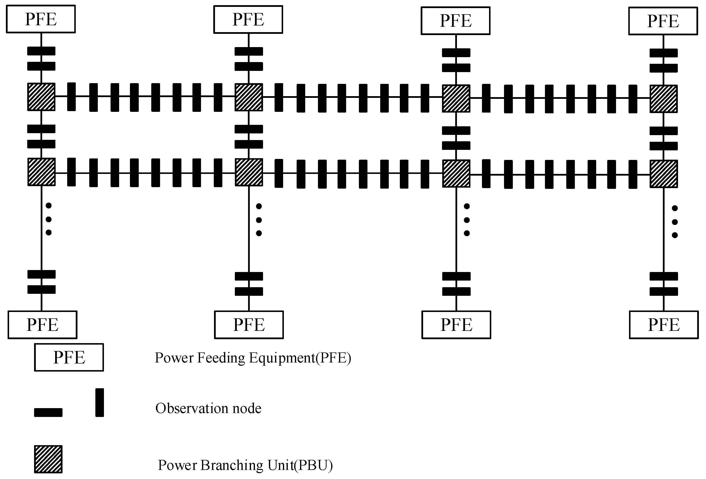
1. Introduction
2. Operating Principle of Active Clamp Dual-Inductor Isolated CS/CS Converter
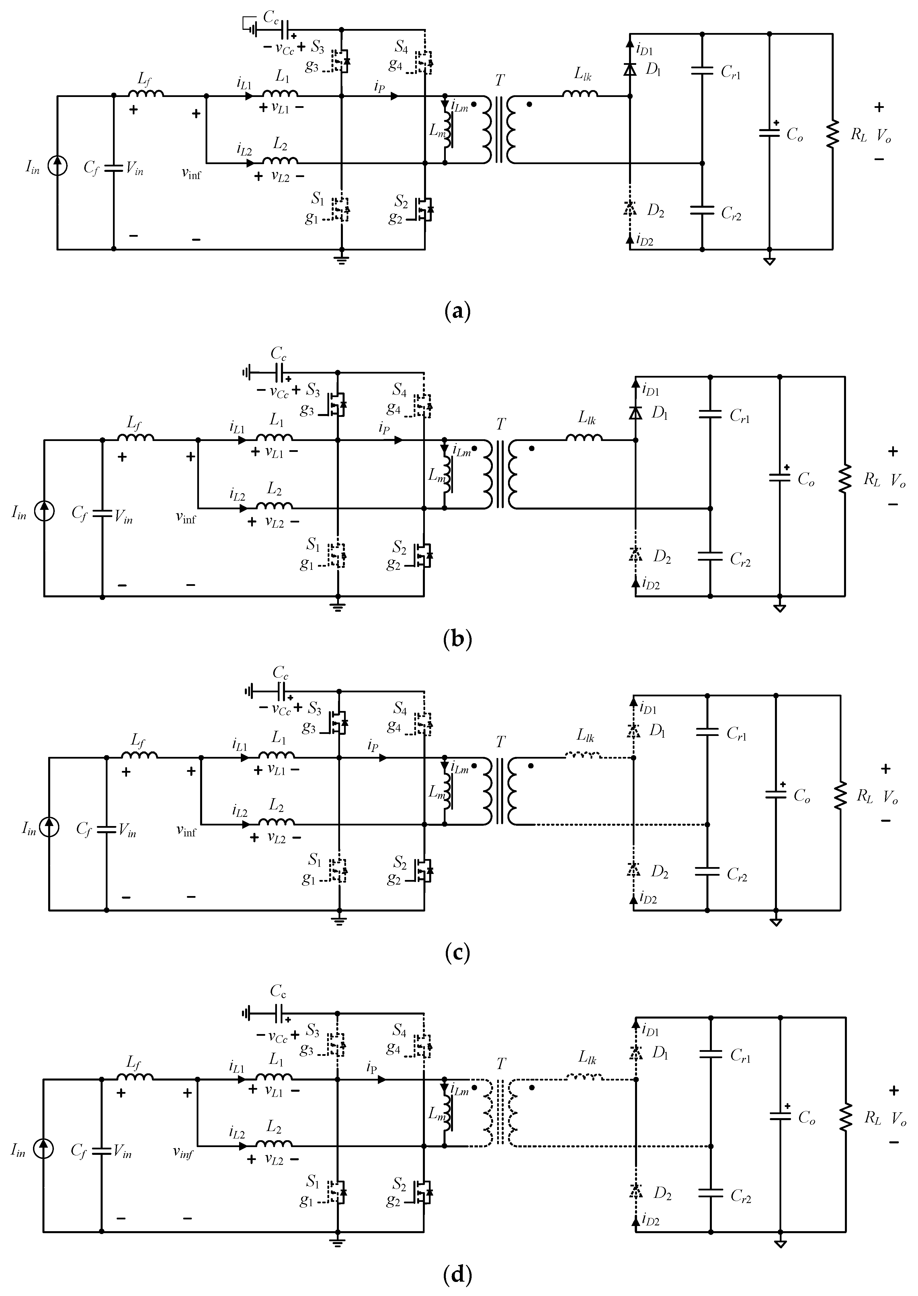
2.1. Operating Principle of Main Circuit Topology and Control Circuit
2.2. Operation Modes Analysis
3. Characteristic and Parameter Design Analysis
3.1. Current Conversion Ratio
3.2. Transformer Turn Ratio Design
3.3. Inductance L1 and L2 Design
3.4. Design of Clamp Capacitor CC, Resonant Capacitor Cr, Resonant Inductor Llk, and Magnetic Inductor Lm
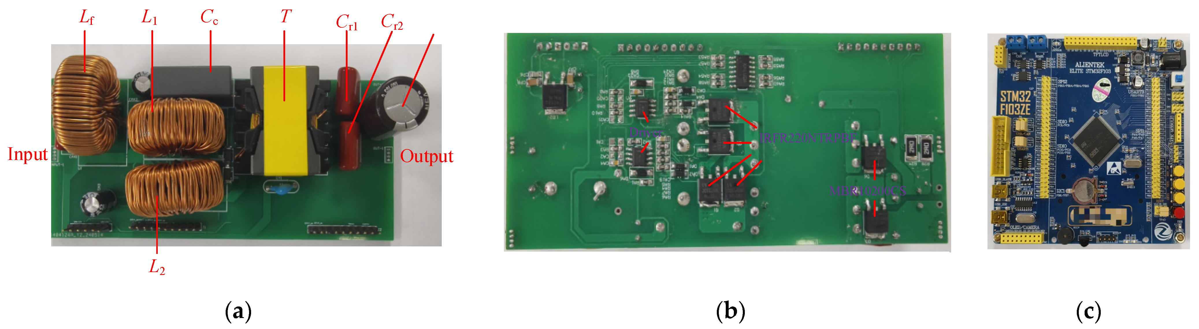
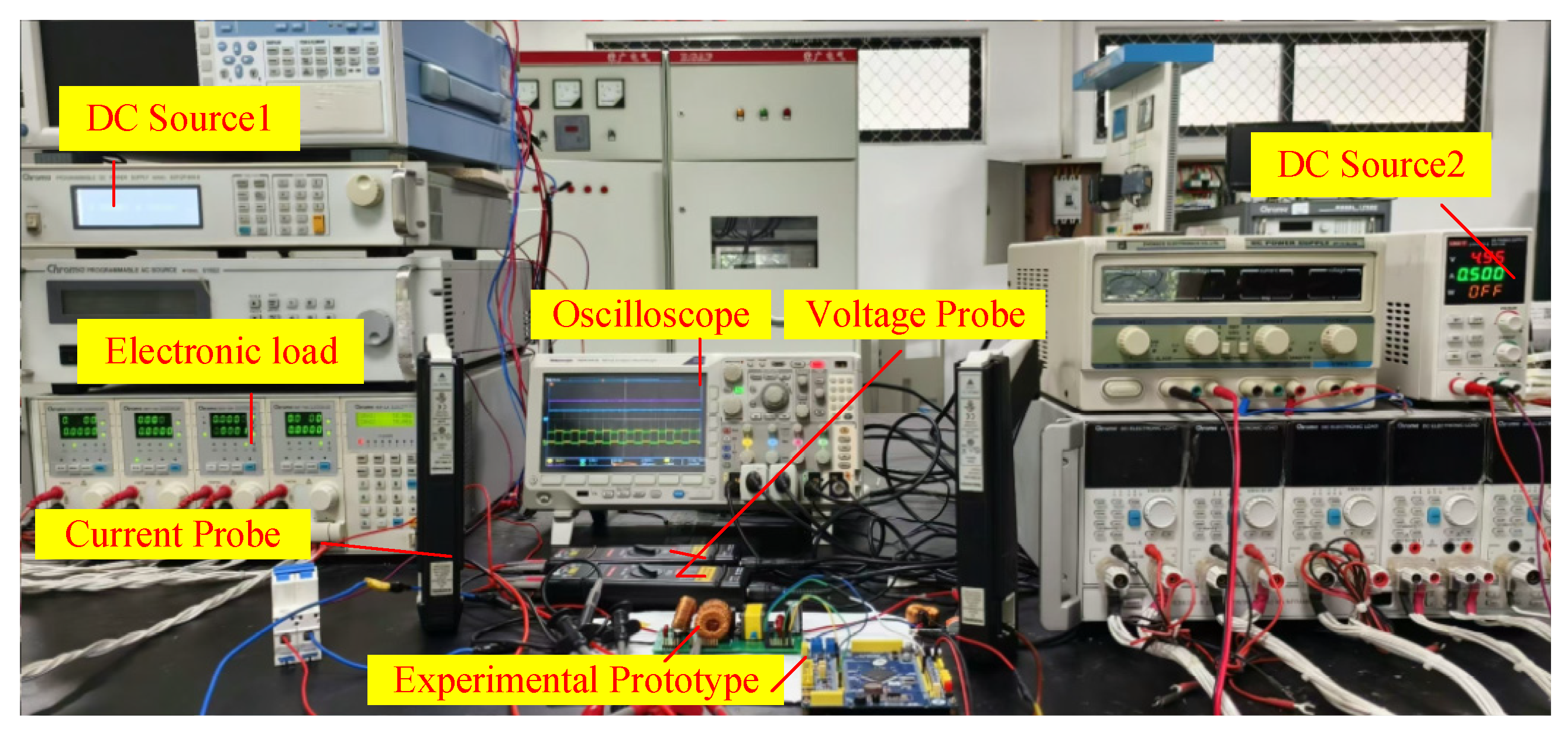
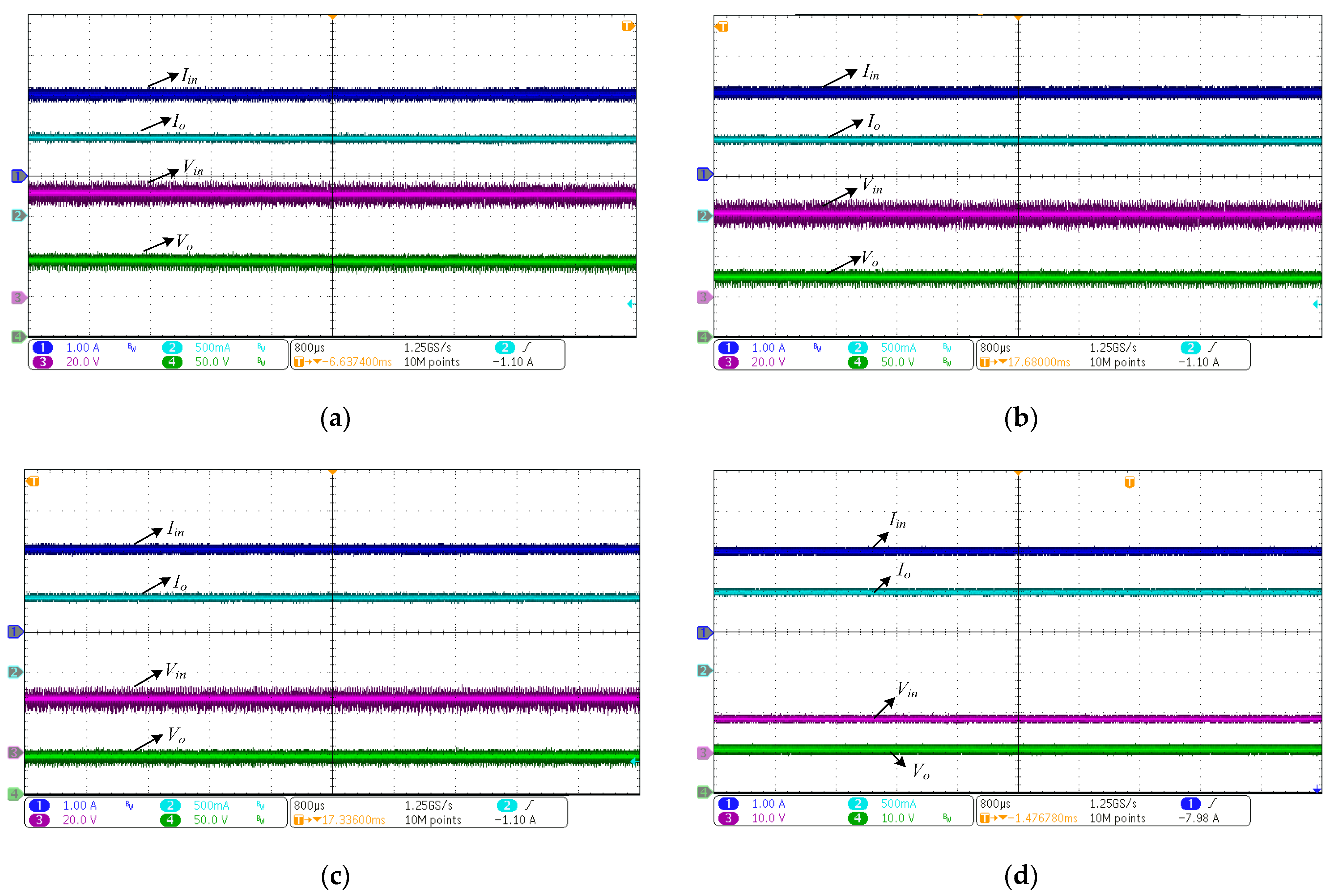
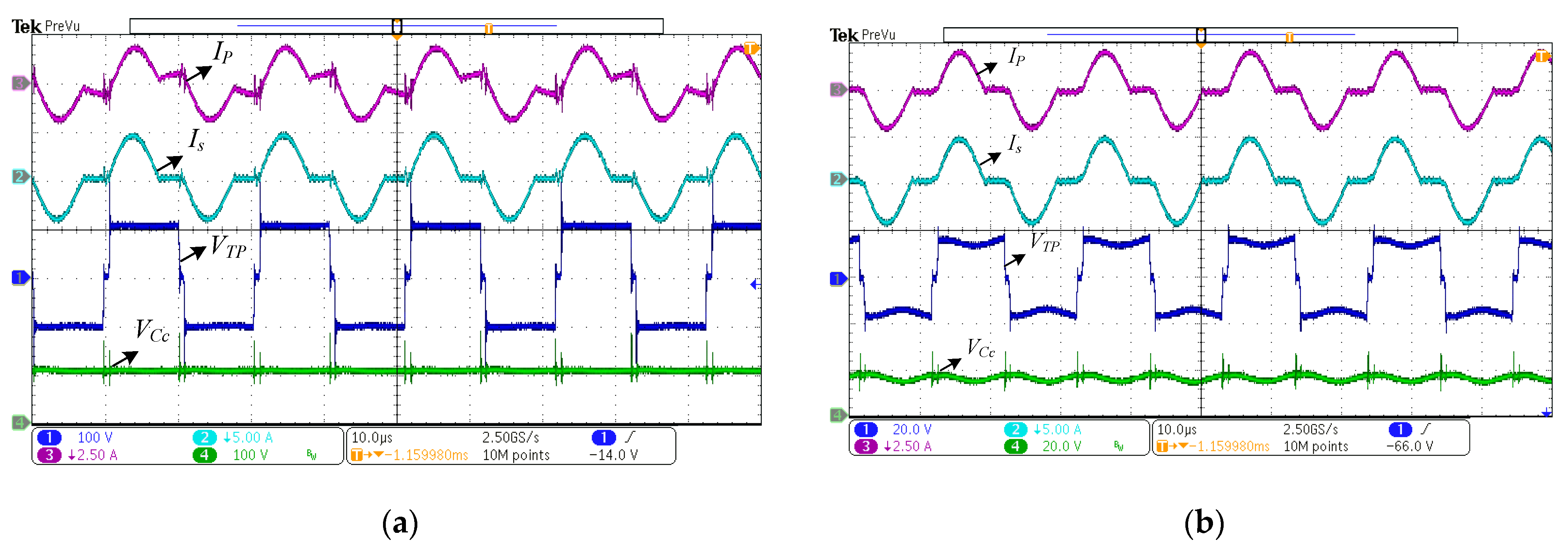
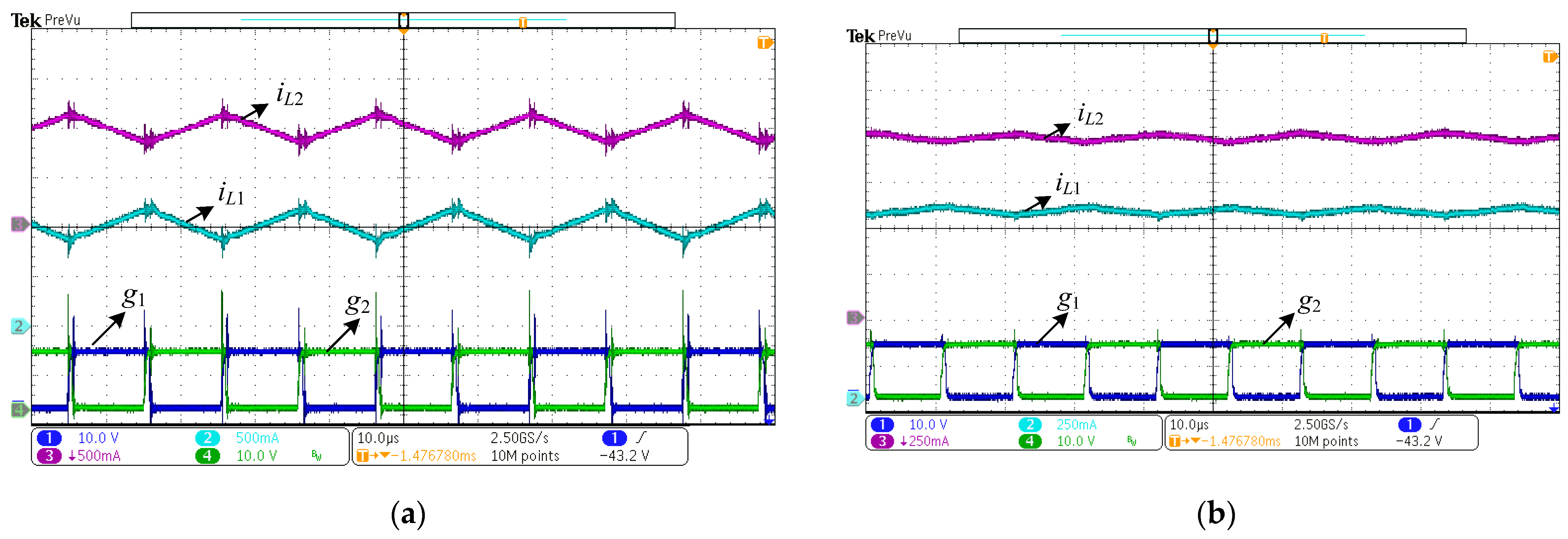
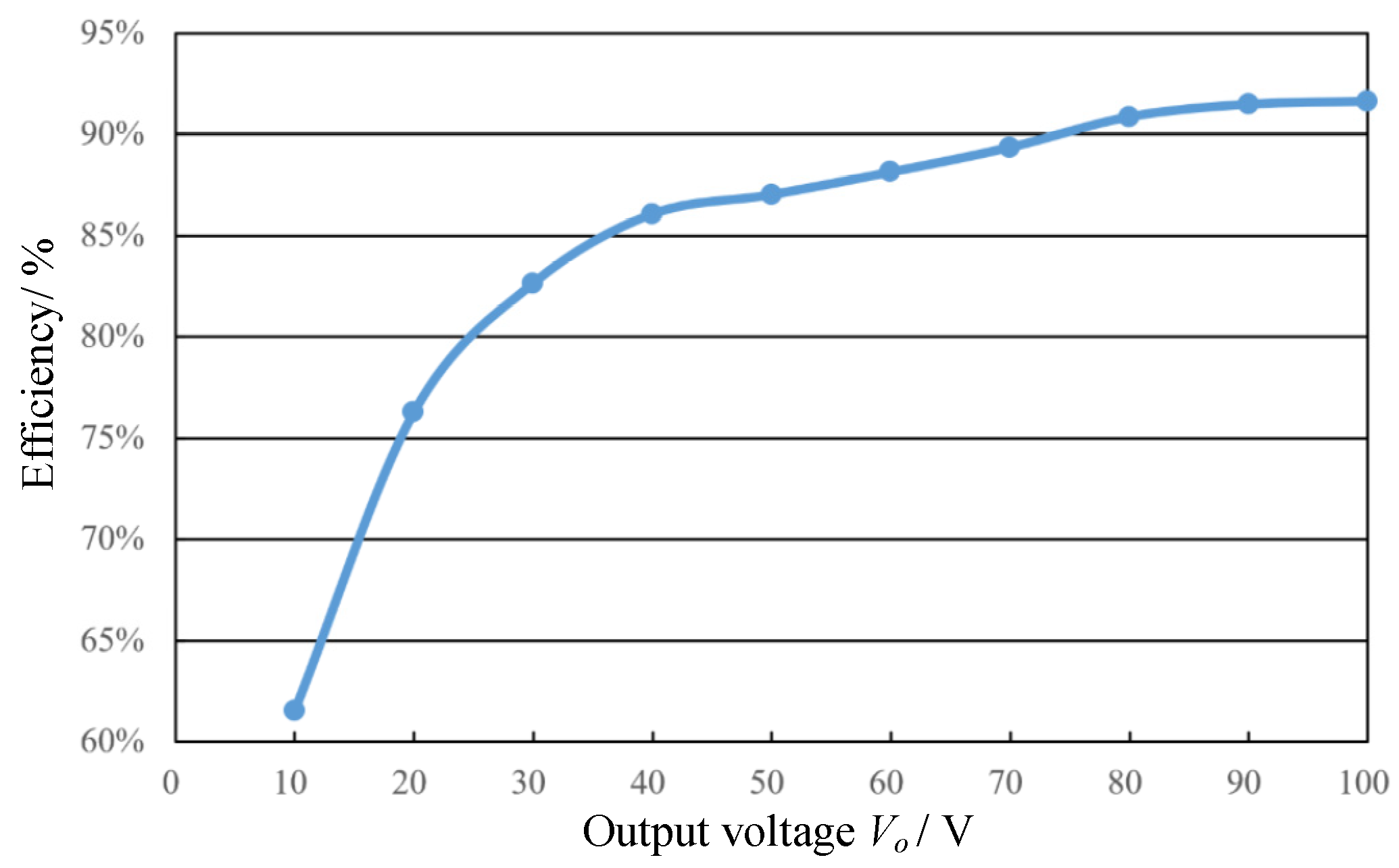
4. Experimental Results
5. Conclusions
Author Contributions
Funding
Data Availability Statement
Conflicts of Interest
References
- Yokota, Y.; Matsuda, T. Underwater Communication Using UAVs to Realize High-Speed AUV Deployment. Remote Sens. 2021, 13, 4173. [Google Scholar] [CrossRef]
- Leslie, M.; Pirenne, B.; Qi, D. Developing in the Dark: Software Development and Quality Assurance for the VENUS/NEPTUNE Canada Cabled Observatories. In Proceedings of the OCEANS 2007, Vancouver, BC, Canada, 29 September–4 October 2007; pp. 1–5. [Google Scholar]
- Sun, Z.; Wang, Z.; Nie, Z.; Zhao, S.; Yu, Y. Improved GNSS/Acoustic Underwater Positioning with Between-Buoy Baseline Constraint. J. Surv. Eng. 2023, 149, 04023012. [Google Scholar] [CrossRef]
- Asakawa, K.; Muramatsu, J.; Kojima, J.; Shirasaki, Y. Feasibility Study on Power Feeding System for Scientific Cable Network ARENA. In Proceedings of the 2003 International Conference Physics and Control (Cat. No.03EX708), Tokyo, Japan, 25–27 June 2003; pp. 307–312. [Google Scholar]
- Asakawa, K.; Kojima, J.; Muramatsu, J.; Takada, T.; Kawaguchi, K.; Mikada, H. Current-to-Current Converter for Scientific Underwater Cable Networks. IEEE J. Ocean. Eng. 2007, 32, 584–592. [Google Scholar] [CrossRef]
- Lu, F.; Zhou, H.; Yue, J.; Peng, X.; He, B.; Wu, Z. Design of an Undersea Power System for the East China Sea Experimental Cabled Seafloor Observatory. In Proceedings of the OCEANS 2013, San Diego, CA, USA, 23–27 September 2013; pp. 1–6. [Google Scholar]
- Ma, R.; Wang, R.; Liu, G.; Chen, H.-H.; Qin, Z. UAV-Assisted Data Collection for Ocean Monitoring Networks. IEEE Netw. 2020, 34, 250–258. [Google Scholar] [CrossRef]
- Ak, N.; Demirbas, A. Promising Sources of Energy in the near Future. Energy Sources Part A Recovery Util. Environ. Eff. 2016, 38, 1730–1738. [Google Scholar] [CrossRef]
- Favali, P.; Beranzoli, L. Seafloor Observatory Science: A Review. Ann. Geophys. 2021, 49, 515–567. [Google Scholar] [CrossRef]
- Barnes, C.R.; NEPTUNE Canada Team. Building the World’s First Regional Cabled Ocean Observatory (NEPTUNE): Realities, Challenges and Opportunities. In Proceedings of the OCEANS 2007, Vancouver, BC, Canada, 29 September–4 October 2007; pp. 1–8. [Google Scholar]
- Asakawa, K.; Muramatsu, J.; Aoyagi, M.; Sasaki, K.; Kawaguchi, K. Feasibility Study on Real-Time Seafloor Glove Monitoring Cable-Network-Power Feeding System. In Proceedings of the 2002 International Symposium on Underwater Technology (Cat. No.02EX556), Tokyo, Japan, 16–19 April 2002; pp. 116–122. [Google Scholar]
- Shirasaki, Y.; Yoshida, M.; Nishida, T.; Kawaguchi, K.; Mikada, H.; Asakawa, K. ARENA: A versatile and multidisciplinary scientific submarine cable network of next generation. In Proceedings of the 2003 International Conference Physics and Control. Proceedings (Cat. No.03EX708), Tokyo, Japan, 25–27 June 2003; pp. 226–231. [Google Scholar]
- Chen, Y.; Howe, B.M.; Yang, C. Actively Controllable Switching for Tree Topology Seafloor Observation Networks. IEEE J. Ocean. Eng. 2015, 40, 993–1002. [Google Scholar] [CrossRef]
- Glenn, S.; Dickey, T.; Parker, B.; Boicourt, W. Long-Term Real-Time Coastal Ocean Observation Networks. Oceanography 2000, 13, 24–34. [Google Scholar] [CrossRef]
- Zhang, Z.; Xu, F.; Bo, J.; Chen, Y.; Yang, C.; Zhang, F. An Active Node Isolating Method Based on Discrete-Voltage Intervention for Seafloor Observation Network. In Proceedings of the OCEANS 2015, Washington, DC, USA, 19–22 October 2015; pp. 48–59. [Google Scholar]
- Asakawa, K.; Kojima, J.; Muramatsu, J.; Takada, T. Novel Current to Current Converter for Mesh-like Scientific Underwater Cable Network-Concept and Preliminary Test Result. In Proceedings of the OCEANS 2003, San Diego, CA, USA, 22–26 September 2003; pp. 1868–1873. [Google Scholar]
- Fan, P.; Xu, Y.; Ren, L.; Tang, Y.; Shi, J.; Li, J. Concept Design of BU for Mesh-like Constant Current Seafloor Observation Networks. In Proceedings of the 2021 IEEE 2nd China International Youth Conference on Electrical Engineering (CIYCEE), Chengdu, China, 15–17 December 2021; pp. 1–6. [Google Scholar]
- Moradisizkoohi, H.; Elsayad, N.; Mohammed, O.A. A Voltage-Quadrupler Interleaved Bidirectional DC–DC Converter with Intrinsic Equal Current Sharing Characteristic for Electric Vehicles. IEEE Trans. Ind. Electron. 2021, 68, 1803–1813. [Google Scholar] [CrossRef]
- Xuewei, P.; Rathore, A.K. Novel Interleaved Bidirectional Snubberless Soft-Switching Current-Fed Full-Bridge Voltage Doubler for Fuel-Cell Vehicles. IEEE Trans. Power Electron. 2013, 28, 5535–5546. [Google Scholar] [CrossRef]
- Zhou, Y.; Zhou, X.; Zhang, Z. Research on Electric Energy Conversion Methods for Small Power Equipment Based on Constant-Current Power Supply with Submarine Optical Cable. In Proceedings of the 2016 International Conference on Integrated Circuits and Microsystems (ICICM), Chengdu, China, 23–25 November 2016; pp. 306–310. [Google Scholar]
- Ninomiya, T.; Higashi, T.; Harada, K.; Tsuya, N.; Gohnai, T.; Honda, Y. Analysis of the Static and Dynamic Characteristics of Push-Pull Parallel Resonant Converters. In Proceedings of the 17th Annual IEEE Power Electronics Specialists Conference, Vancouver, BC, Canada, 23–27 June 1986; pp. 367–374. [Google Scholar]
- Saha, T.; Wang, H.; Riar, B.; Zane, R. Analysis and Design of a Parallel Resonant Converter for Constant Current Input to Constant Voltage Output DC-DC Converter Over Wide Load Range. In Proceedings of the 2018 International Power Electronics Conference (IPEC-Niigata 2018-ECCE Asia), Niigata, Japan, 20–24 May 2018; pp. 4074–4079. [Google Scholar]
- Modepalli, K.; Mohammadpour, A.; Li, T.; Parsa, L. Three-Phase Current-Fed Isolated DC–DC Converter with Zero-Current Switching. IEEE Trans. Ind. Appl. 2017, 53, 242–250. [Google Scholar] [CrossRef]
- Zhang, Z.; Zhou, X.; Wang, X.; Wu, T. Design, Analysis, and Modeling of an Isolated Constant-Current to Constant-Voltage Converter in Cabled Underwater Information Networks. Electronics 2019, 8, 961. [Google Scholar] [CrossRef]
- Wang, L.; Wang, X.; Zhou, X.; Chen, S. Design and Analysis of an Isolated Constant Current to Constant Current Converter with Capacitor Transferring Energy. In Proceedings of the 2020 IEEE 1st China International Youth Conference on Electrical Engineering (CIYCEE), Wuhan, China, 1–4 November 2020; pp. 1–7. [Google Scholar]


| Design Parameter | Value |
|---|---|
| Input current Iin/A | 2 |
| Switching frequency fs/kHz | 50 |
| Output current value Io/A | 1 |
| Rated output voltage Vo/V | 100 |
| Inductance L1 and L2/mH | 2 |
| Transformer T turn ratio | 2.2 |
| Magnetic inductance Lm/μH | 300 |
| Secondary side leakage inductance Llk/μH | 1.5 |
| Resonant capacitor Cr1 and Cr2/μF | 1 |
| Clamp capacitor CC/μF | 1 |
| Main switches S1, S2, S3, S4 | IRFR220NTRPBF |
| Schottky diode D1 and D2 | MBR10200CS |
| Output filter capacitor Co/μF | 100 |
| Equipment Variety | Equipment Model | Function |
|---|---|---|
| DC Power Source 1 | Chroma 62012P-600-8 | Provide input power for the proposed converter. |
| DC Power Source 2 | UNI-TREND UTP1310-II | Provide power supply for the control board. |
| DC Electronic load | Chroma 6314A + 63115A + 63110A | One channel provides output load for output current source, another channel works with the DC power source 1 to provide the input current source. |
| Oscilloscope | Tektronix DPO3014 | Measure and display waveforms. |
| Voltage Probe | RIGOL RP1025D | Measure voltage waveforms. |
| Current Probe | Tektronix TCP0150 | Measure current waveforms. |
| Digital Multimeter | Fluke 17B | Measure input voltage, output voltage, input current, and output current of experimental board. |
Disclaimer/Publisher’s Note: The statements, opinions and data contained in all publications are solely those of the individual author(s) and contributor(s) and not of MDPI and/or the editor(s). MDPI and/or the editor(s) disclaim responsibility for any injury to people or property resulting from any ideas, methods, instructions or products referred to in the content. |
© 2024 by the authors. Licensee MDPI, Basel, Switzerland. This article is an open access article distributed under the terms and conditions of the Creative Commons Attribution (CC BY) license (https://creativecommons.org/licenses/by/4.0/).
Share and Cite
Yan, T.; Chen, W.; Zhou, Y.; Lin, D.; Tian, J.; Zhou, G. An Active Clamp Dual-Inductor Isolated Current Source to Current Source Converter with Wide Output Voltage Range. Electronics 2024, 13, 2925. https://doi.org/10.3390/electronics13152925
Yan T, Chen W, Zhou Y, Lin D, Tian J, Zhou G. An Active Clamp Dual-Inductor Isolated Current Source to Current Source Converter with Wide Output Voltage Range. Electronics. 2024; 13(15):2925. https://doi.org/10.3390/electronics13152925
Chicago/Turabian StyleYan, Tiesheng, Wenyuan Chen, Yu Zhou, Dong Lin, Jun Tian, and Guohua Zhou. 2024. "An Active Clamp Dual-Inductor Isolated Current Source to Current Source Converter with Wide Output Voltage Range" Electronics 13, no. 15: 2925. https://doi.org/10.3390/electronics13152925
APA StyleYan, T., Chen, W., Zhou, Y., Lin, D., Tian, J., & Zhou, G. (2024). An Active Clamp Dual-Inductor Isolated Current Source to Current Source Converter with Wide Output Voltage Range. Electronics, 13(15), 2925. https://doi.org/10.3390/electronics13152925