Article

A Broadband Meta-Absorber for Curved Terahertz Stealth Applications

1
School of Electronic Engineering, Beijing University of Posts and Telecommunications, Beijing 100876, China
2
Department of Telecommunication Engineering, Mehran University of Engineering and Technology, Jamshoro 76062, Pakistan
3
Beijing Key Laboratory of Work Safety and Intelligent Monitoring, Beijing University of Posts and Telecommunications, Beijing 100876, China
*
Author to whom correspondence should be addressed.
Electronics 2024, 13(15), 2966; https://doi.org/10.3390/electronics13152966 (registering DOI)
Submission received: 12 July 2024 / Revised: 23 July 2024 / Accepted: 25 July 2024 / Published: 27 July 2024
(This article belongs to the Section Microwave and Wireless Communications)

Abstract

:
Metasurface absorbers have shown significant potential in stealth applications due to their adaptability and capacity to reduce the backscattering of electromagnetic (EM) waves. Nevertheless, due to the materials used in the terahertz (THz) range, simultaneously achieving excellent stealth performance in ultrawideband remains an important and difficult challenge to overcome. In this study, an ultrawideband absorber is proposed based on indium tin oxide (ITO) and polyethylene-terephthalate (PET), with a structure thickness of only 0.16λ. ITO sheets are utilized to achieve broad-spectrum, optical transparency and flexibility of the metasurface. The results show that absorption higher than 90% can be achieved in the frequency band ranging from 1.75 to 5 THz under normal TE and TM polarizations, which covers a wide THz band. The structure is insensitive to polarization angles and exhibits 97% relative bandwidth above 90% efficiency up to an oblique incident angle of 60°. To further validate the efficiency of the absorption performance, the radar cross-section (RCS) reduction investigation was performed on both planar and conformal configurations. The findings show that under normal incidence EM waves, both flat and curved surfaces can achieve RCS reduction of over 10 dB, covering an extremely wide frequency range of 1.75 to 5 THz. The metasurface presented in this study exhibits significant potential for use in several THz applications, including flexible electronic devices and stealth aircraft windows.

1. Introduction

In the field of modern radar and communication systems, the efforts to reduce electromagnetic (EM) interference have resulted in the creation of inventive technologies with the goal of mitigating interference and enhancing overall system performance [1]. Metasurfaces (MSs) have emerged as novel solutions among these technologies, providing unprecedented versatility and functionality [2,3]. Subwavelength meta-atoms, organized in periodic or quasi-periodic configurations, have significantly transformed the control and manipulation of radiation. MSs have found extensive utilization in various applications, specifically in the field of stealth technology, with the main objective of minimizing radar cross-section (RCS), to prevent the target from being detected [4]. There are two techniques to perform RCS reduction through MSs: (i) diffusion and (ii) absorption. The first approach scatters the reflected EM waves away from the direction of the source using coding MSs that works on the principle of phase discontinuity [5]. Another approach for RCS reduction is absorbing the incident energy [6,7]. In the realm of EM waves, Landy et al. introduced the concept of a perfect metasurface absorber (PMA) that uses split-ring resonators to attain an absorptivity of 99% at a given frequency [8]. Subsequently, several PMAs have been developed and analyzed, including the visible [9], microwave regions [10], and terahertz regions [11,12]. However, a significant drawback of most MSAs is their confined bandwidth, which poses challenges for their real-world implementation. To overcome these limitations, there are two primary methods. The first approach refers to the occurrence of several absorption peaks that are due to the arrangement of multilayered structures [13,14] or the existence of many resonators on a single layer [15]. However, it suffers the shortcomings in adaptability, transparency, and high pricing. The second approach involves enhancing the resistance of a periodic conductive design to achieve the added advantage of dissipating energy by the use of lumped resistors [16,17], employing resistive inks [18] or utilization of resistive films [19,20]. By loading lumped resistors, it can lead to a parasitic effect at high frequencies and increase processing issues. On the other hand, resistive films offer several benefits, including low cost, ease of production, and great flexibility. Also, resistive sheets, such as indium tin oxide (ITO), have the unique feature of enabling both transparency and flexibility [21].
The potential of resistive films as THz absorbers has led to an increase in research and development of broadband absorbers in recent years. For the frequency range of 0.4–1 THz, Junjie et al. created a transparent and flexible absorber using an ITO-PVC structure that was more than 80% efficient [22]. However, the structure lacks oblique stability due to higher thickness. Adding to that, Jinming et al. created an ITO-based meta-absorber capable of absorbing a wide range of frequencies from 0.4 to 1.3 THz, with an average absorption of 80% [23]. Wei Ying integrated different absorbers into a hybrid flexible array and successfully reduced RCS ranging from 0.55 to 0.7 THz [24]. Furthermore, Xin Yan presented a broadband flexible absorber with wide-angle stability and RCS reduction characteristics [25]. Nevertheless, the low efficiency and complex patterns result in a substantial rise in the effort required to manufacture and implement these structures in real-world scenarios. Moreover, ITO-based THz metasurface absorbers’ capability to reduce RCS is rarely studied in the available research.
Based on ITO-PET, this study presents a polarization-insensitive absorber in the THz regime that has a low profile, is optically transparent, flexible, and has a wide absorption bandwidth. The working mechanism of the meta-absorber and the impact of various structural parameters on the properties of the metasurface are analyzed. Additionally, a high efficiency of above 90° is maintained across the entire absorptivity range, with oblique incidence angles of 60°. The proposed structure is novel in the following ways: (i) The utilization of a simple single element consisting of a slot in the ITO sheet to achieve absorption over a broadband (fractional bandwidth, FBW = 97%). (ii) The proposed structure exhibits a wide frequency range for reducing the RCS by 10 dB, spanning from 1.75 THz to 5 THz. Furthermore, the performance of the structure has shown resistance on curved surfaces.

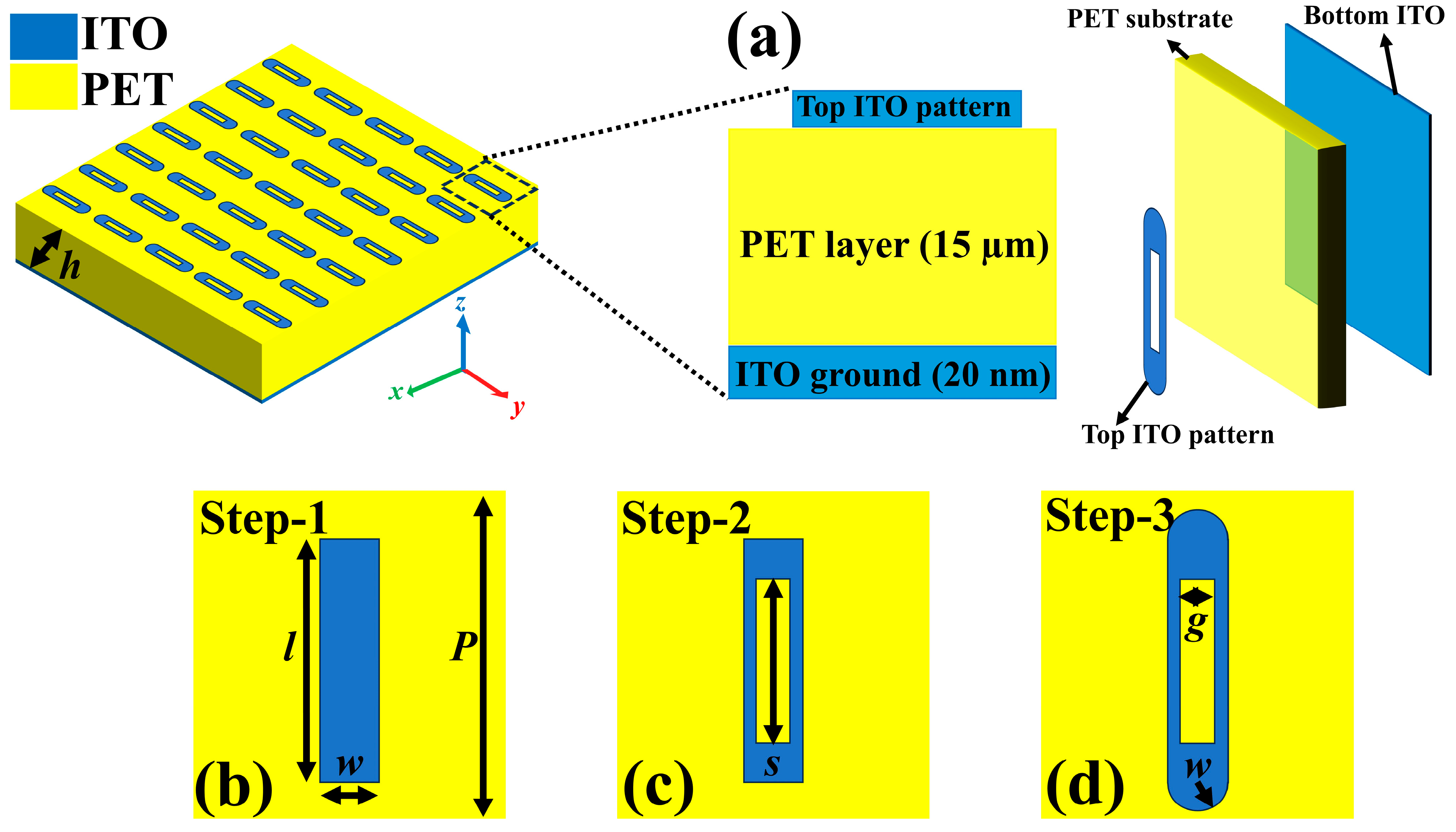
2. Design and Simulation Setup

To achieve absorption and polarization insensitivity, it is necessary to create structures that are symmetric in design. Figure 1a illustrates the schematics of a suggested absorber, together with the symmetric structure of its meta-atom. Additionally, the progressive formation of the meta-atom is depicted in Figure 1b–d and labeled as steps 1, 2, and 3, respectively. Regions in yellow and blue represent PET and ITO layers, respectively. The meta-atom exhibits a sandwich-like configuration, comprising three layers with a periodicity of P = 55 µm. The top surface consists of a patterned ITO resonator, which is printed onto a flexible PET substrate. The gaps between the ITO pattern are w = 8 µm, l = 30 µm, s = 24 µm, and g = 6 µm. The ground plane, on the other hand, is a continuous ITO layer with a sheet resistance of 80 ohm/square and a thickness of 20 nm. The PET sheet has a loss tangent of 0.06 and a relative permittivity of 3.0 with a thickness “h” of 15 µm. The commercially available optically transparent ITO-PET films were utilized in the design. The CST Studio Suite 2020 was used with a frequency domain solver to create the design of atom structures and simulate their EM characteristics using unit cell boundary conditions and Floquet port.

3. Results and Analysis

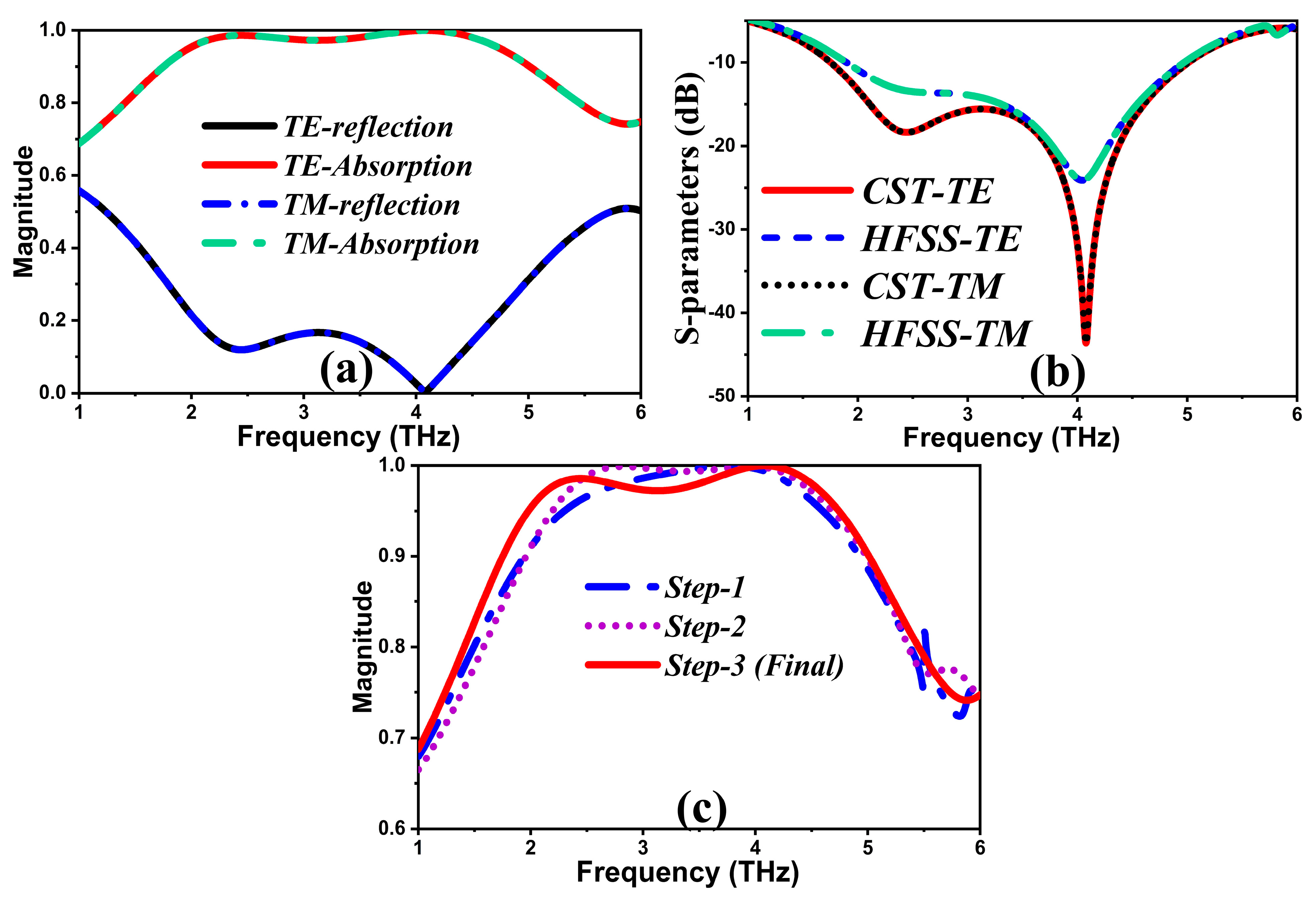
3.1. Absorption Characteristics

The absorption characteristics of a suggested configuration can be obtained by analyzing the reflection and transmission of EM signals. Thus, the absorption can be determined as follows [26]:
A ( ω ) = 1 R ( ω ) T ( ω ) = 1 | S 11 | 2 | S 21 | 2
Here, the absorptivity is denoted by A ( ω ) , whereas the reflectivity and transmittance are denoted by R ( ω ) = S 11 2 and T ( ω ) = S 21 2 , respectively. The S 11 2 is considered as the result of both co-polarized and cross-polarized components. The co-polarized component result is obtained when both the incident and reflected EM wave are either TE-polarized or TM-polarized. In contrast, the cross-polarized component value is acquired when the incoming wave is polarized in the TE mode and the reflected wave is polarized in the TM mode, or vice versa. Using continuous ITO film as the bottom layer results in zero transmittance T ( ω ) for the design. Consequently, we can simplify Equation (1) as follows:
A ( ω ) = 1 R ( ω ) = 1 | S 11 | 2
The simulated results of absorption and reflection for TE and TM modes under normal incidence waves are shown in Figure 2a. The TE polarization is a representation of an incident wave that has the orientation of its electric field along the y-direction. On the other hand, the TM polarization has the electric field oriented along the x-direction. The results indicate the same response for TE and TM modes, where reflection coefficient remains below 0.3 dB across a broad frequency range of 1.75 THz to 5 THz, while the absorptivity exceeds 90%. At 2.36 and 4.09 THz, the peak absorption values are 99% and 100%, respectively. Moreover, the performance of a proposed design is validated in HFSS software. The simulated results from both software packages show good agreement, as seen in Figure 2b. The slight difference between the simulated results of CST and HFSS is due to the different numerical techniques employed by the two software. Both the results cover the desired bandwidth of 1.75 THz to 5 THz. Adding to that, the absorption properties for the design sequence of the suggested structure are illustrated in Figure 2c. As we move towards the final step of the design process, the absorption bandwidth increases in an orderly manner.

3.2. Absorption Characteristics

Impedance matching is a crucial factor in determining absorption behavior. The impedance of a meta-absorber depends upon its effective permittivity and permeability. The calculated normalized input impedance (Zin) of the proposed design, which includes an ITO ground layer, can be derived from the simulated S-parameters as follows:
Z i n = μ ε = ( 1 + S 11 ) 2 ( 1 S 11 ) 2
The maximum absorption will occur when the normalized impedance of the absorber is equal to the free-space impedance. In other words, when the real part of the normalized impedance (Z′) is close to 1 and the imaginary part (Z″) is close to 0, maximum absorption will occur. The plot in Figure 3a displays the normalized input impedance of the proposed meta-absorber. It indicates that the real part of the normalized input impedance is nearly 1 and the imaginary part is approximately 0 within the frequency range of 1.75 THz to 5 THz. This observation aligns with the principles of impedance matching theory. In order to gain a deeper understanding of the absorption mechanism for this structure, the surface current distributions at 4.09 THz resonant frequency are examined in Figure 3b,c. The resonances are produced by either the electric or magnetic resonance of a given structure. When the surface current distribution on the top pattern and bottom ground is parallel, then electric resonance will be generated. On the other hand, when the current is induced on the top and bottom layers in the opposite direction, then magnetic resonance will occur. At 4.09 THz, the top layer surface currents are opposite to those on the ground, generating magnetic resonance, which agrees with the absorption operating principle [27].

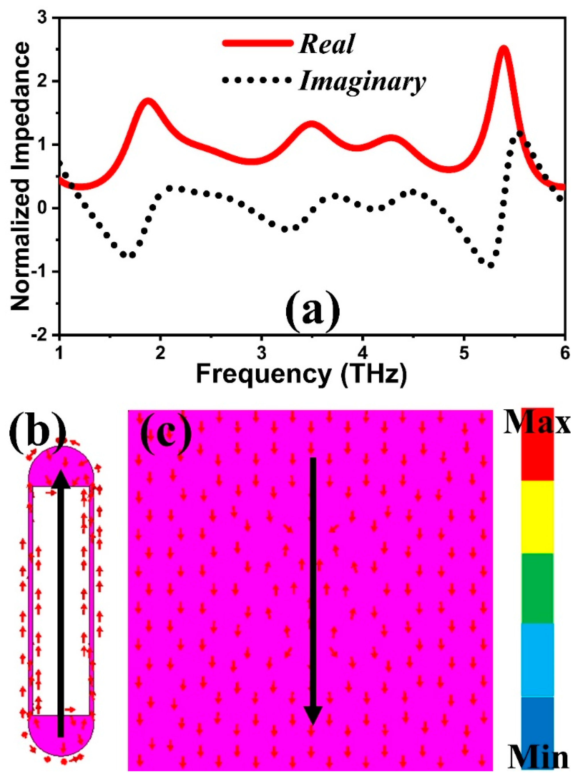
3.3. Equivalent Circuit Model

The comprehensive analysis of the broadband response of a suggested absorber can be explained by employing an equivalent circuit, which can be modeled using a transmission line method (TLM). The absorber structure does not consist of metal, and the resistive property is provided by the ITO resonators. The impedance being offered by the PET layer can be represented by Zc = Z 0 / ε , which is terminated by the bottom ITO layer “Rg”. The equation presented can be used to compute the impedance at the input terminal of the transmission line [24]:
Z 1 = Z c R g + j Z c tan ( β h ) Z c + j R g tan ( β h )
Here, Z c , β, and h are characteristic impedance, phase constant, and thickness of PET dielectric substrate, respectively. The upper layer of ITO can be represented as a series configuration consisting of resistance R, inductance L, and capacitance C. On the other hand, the lower layer of ITO can be defined as the equivalent resistance Rg. ZR represents the impedance provided by the resonance circuit. The total input impedance can be calculated as Zin = ZR||Z1. Finally, the calculation of the reflection coefficient can be determined as follows:
Γ = Z i n Z o Z i n + Z o
The equivalent circuit model of the proposed absorber is developed and simulated using Keysight’s advanced design system (ADS) simulation tool, shown in Figure 4a. The values of components are as follows: R = 15 Ω, L = 0.035 nH, and C = 0.00075 pF. Figure 4b illustrates the S11 of the equivalent circuit and CST software. It is noted that both tools show similar S11 characteristics (resonating at 2.36 and 4.09 THz), which further increases confidence that the proposed design will perform as expected in a real-world setting.

4. Effect of Model Parameters on Absorption Parameters

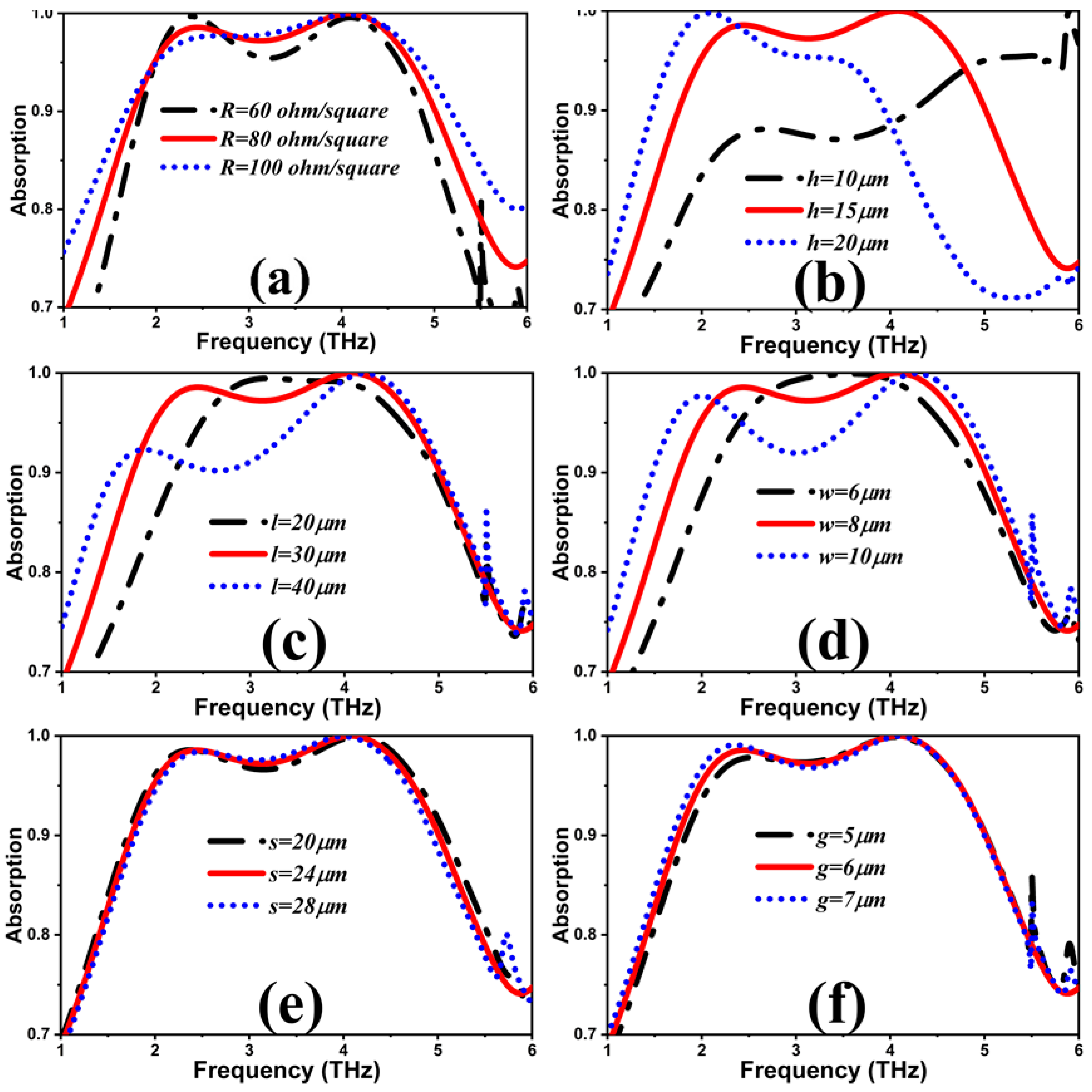
4.1. ITO Sheet Resistance

The impact of the ITO sheet resistance (R) on the MS absorption spectrum is seen in Figure 5a. An optimal ITO resistance results in a better absorption bandwidth due to the impedance matching, as seen in the figure. However, a further increase in sheet resistance greater than the optimal value will affect the impedance mismatch, resulting in efficiency decreasing at the first resonant peak. Therefore, the aforementioned analysis findings suggest that the absorption efficiency and bandwidth can be controlled by modifying the resistance of ITO sheets.

4.2. Substrate Height

The impact of different thicknesses of the dielectric layer on the absorption properties was also examined, as depicted in Figure 5b. It is a crucial factor in developing absorbers as it determines the conformability and the low-profile characteristics of the proposed structure. It is observed that increasing or decreasing the thickness from the optimal value will badly affect the efficiency as well as operating bandwidth. This is due to the height of the substrate influencing the effective refractive index experienced by the EM waves interacting with the MS. Therefore, the PET having a thickness of 15 µm is selected for designing the absorber presented in this work as it provides near-unity absorption in a broad frequency spectrum.

4.3. Geometric Parameters of ITO Pattern

An analysis is conducted on the impact of the geometric parameters (l, w, s, and g) of the ITO pattern layer on the absorption efficiency and bandwidth. This analysis is illustrated in Figure 5c–f. As depicted in Figure 5c, the absorption bandwidth increases while efficiency gradually drops as the value of l increases. Therefore, the optimum value for l, considering both efficiency and working bandwidth, is 30 µm. Figure 5d demonstrates that for w < 8 µm, there is a drop in the absorption bandwidth. When the w ˃ 8 µm, the efficiency decreases as the bandwidth increases. The main reason behind the variations in absorption spectrum due to change in length and width of the resistive structure is because the resistive pattern changes the distribution of the electric and magnetic fields within the unit cell. This redistribution affects the local resonant conditions, leading to a shift in resonant frequency. In Figure 5e,f, altering the values of “s” and “g” will have minimal impact, despite a modest change in the frequency band. The analysis conducted above reveals that the most favorable values for l, w, s, and g are 30, 8, 24, and 6 µm, respectively.

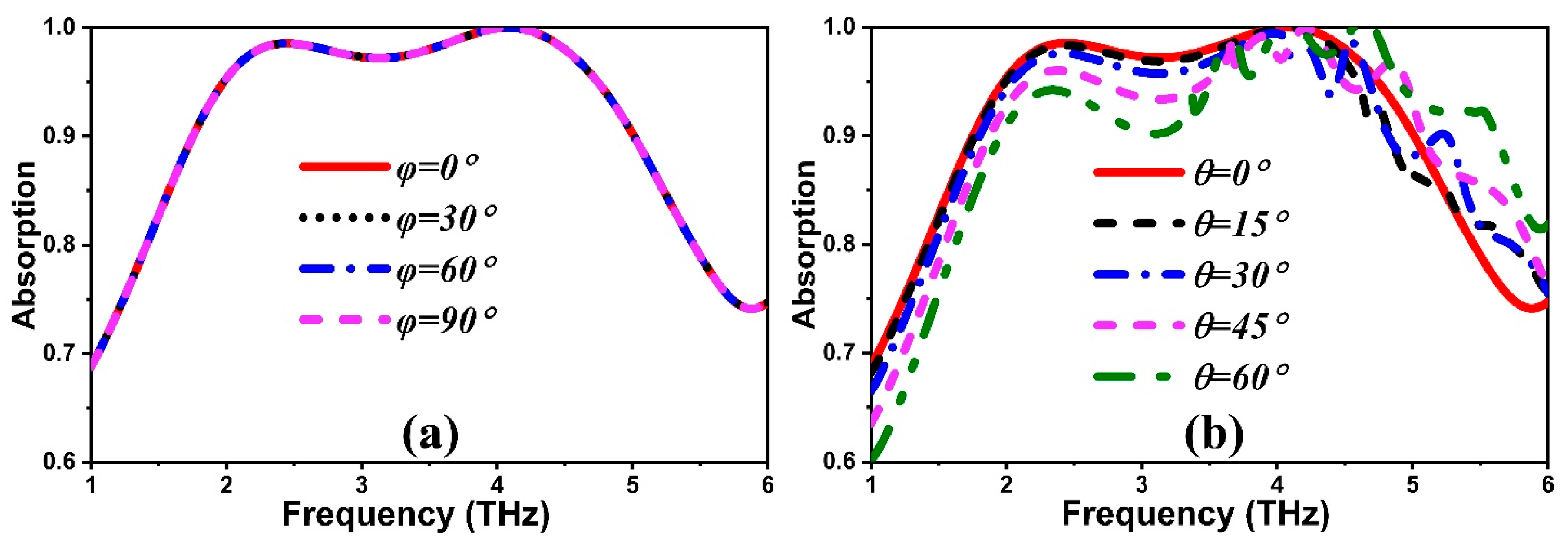
5. Angular Stability

In real-world applications, EM waves strike the surface of the structure at various angles. An optimal absorber should effectively absorb EM radiation regardless of the polarization angle or incidence angle. Hence, we conducted a sequence of numerical simulations to evaluate the performance of the suggested structure under different polarizations and oblique incidence angles. Figure 6a illustrates the absorption spectra of a suggested meta-absorber. It is evident that the absorption of the varying polarization angles (ϕ) ranging from 0 to 90° is constant. The structure exhibits polarization angle insensitivity as a result of its symmetric nature along the x and y-axes. Next, absorptivity spectra under different oblique incidences are depicted in Figure 6b. It can be observed that the absorption efficiency remains consistently above 90% at incident angles ranging from 0 to 60°, and the absorption bandwidth remains almost unchanged. The result demonstrates that the suggested design exhibits excellent absorption capabilities and maintains a steady operating bandwidth even at large angles.

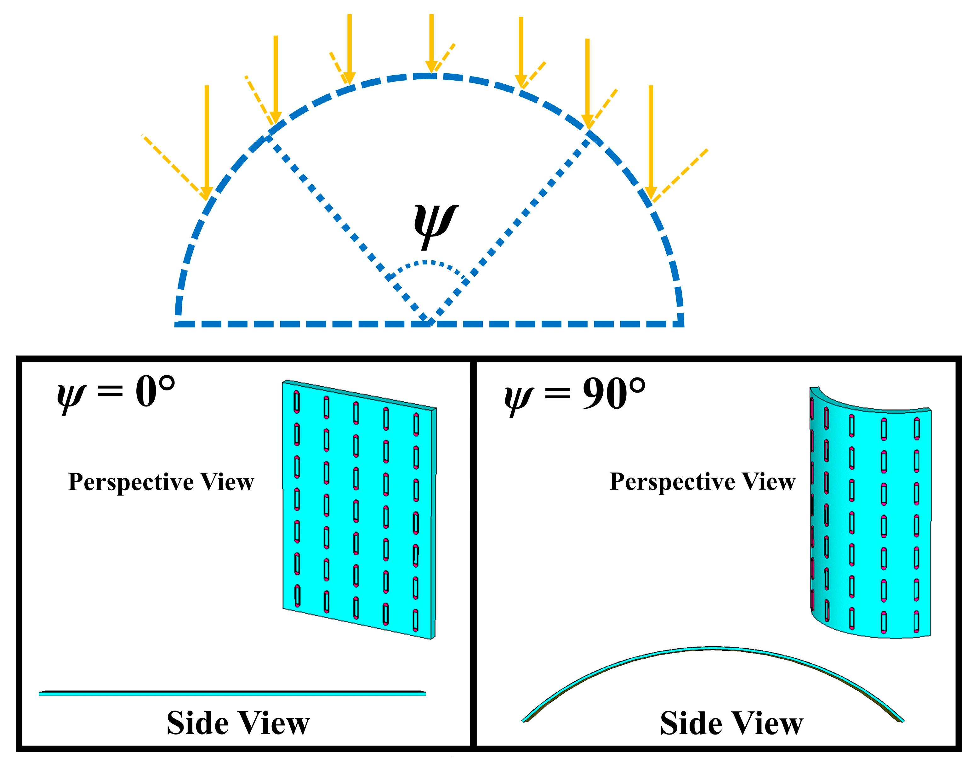
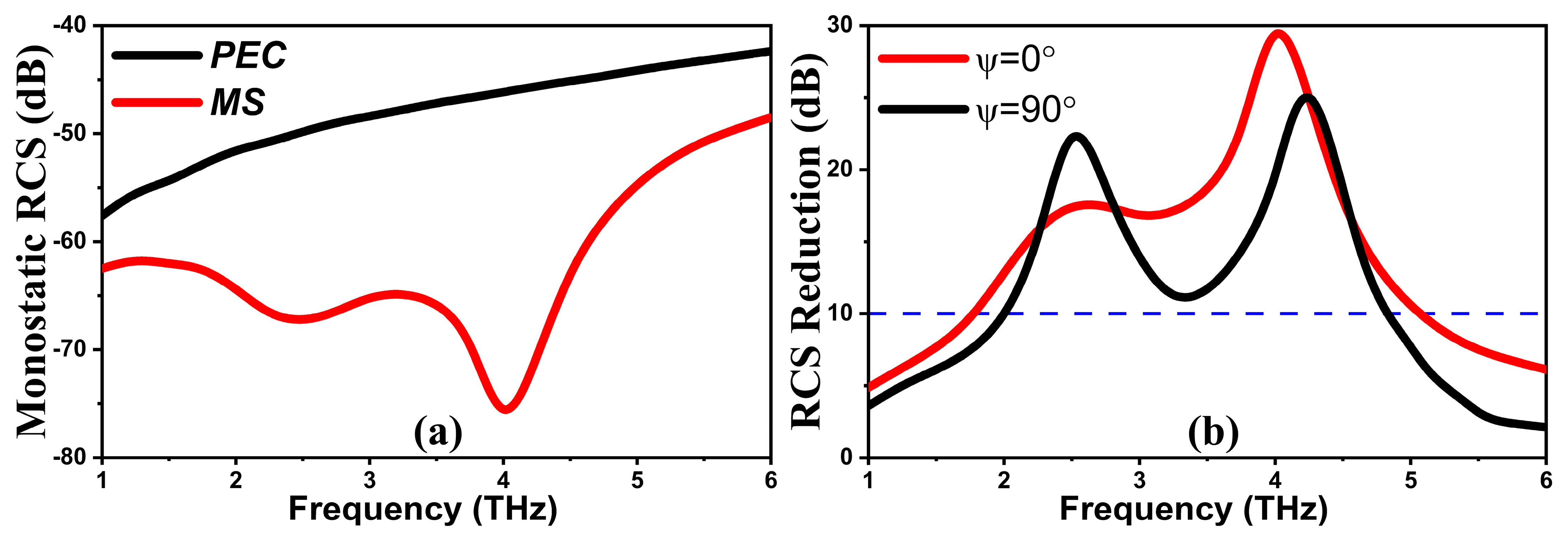
6. Radar Cross-Section (RCS) Analysis of Planar and Curved Structure

Analyzing the reduction in RCS can be used to assess the absorption capabilities of a structure. Therefore, in order to evaluate RCS suppression capability for planar and conformal configuration with convex bending angle (ψ), a meta-atom array with a finite size of 5 × 7 is created, as shown in Figure 7. For comparison, a copper plate with a thickness of 0.035 µm and an electric conductivity of 5.8 × 10⁷ S/m is designed to be similar in shape and size to the proposed absorber. During the full-wave simulation in CST software, a plane wave with open boundary conditions is applied to the surface of the structure.
Figure 8a depicts the simulated monostatic RCS of the plain copper sheet and RCS of a plain MS under normal incident EM wave. It is observed that the RCS of an MS is found to be substantially lower than that of the flat copper sheet. Furthermore, Figure 8b shows the RCS reduction for planar and conformal configuration. Between 1.75 THz and 5 THz, a reduction of more than 10 dB is observed when the surface bending angle (ψ) is 0°. Adding to that, it is noticeable that a curved surface (ψ = 90°) can still keep the RCS reduction above 10 dB within the specified frequency range. Note that the simulated findings can be validated through measurements in real conditions by using a fiber-coupled THz time-domain spectroscopy system in a reflection mode [25]. A major feature of this system is that the THz emission and detection are arranged in the optical guide, respectively. The angle between them can be adjusted by rotating the two optical guides. A copper mirror with the same size can be used as the reference to normalize the power reflectance of the sample. Table 1 compares the proposed structure with some of the recently published works. As can be seen from this table, the proposed structure is superior to previous structures in terms of flexibility, low profile, broad bandwidth, and insensitivity to wide incident wave angles.

7. Conclusions

This research presents a low-profile MS that effectively absorbs ultrawideband signals in the THz frequency range. Numerical simulations reveal that a combination of an ITO reflective backplane, a PET layer, and an ITO resistive layer can achieve absorption efficiencies of above 90% from 1.75 THz to 5 THz. The absorber’s stable response is achieved over a wide frequency range of 97% regardless of the polarization, due to its symmetric geometry, whereas absorptivity of more than 90% is realized in the abovementioned frequency band under oblique incidents up to 60°. In addition, this study thoroughly examines the structure’s monostatic RCS reduction capability and observes that it can offer over 10 dB RCS reduction in both planar and conformal designs. This approach holds significant potential in various applications, including radar arrays, windows for stealth aircraft, and rooms designed for EM shielding.

Author Contributions

Conceptualization, J.Y.; methodology, S.H.; software, S.H.; supervision, F.A.U.; validation, W.Y.; formal analysis, F.A.U.; funding acquisition, W.Y.; investigation, A.M.; resources, J.Y.; data curation, J.Y.; writing—original draft, S.H.; writing—review and editing, S.H.; visualization, A.M. All authors have read and agreed to the published version of the manuscript.

Funding

The article processing fee of this work was supported by the National Natural Science Foundation of China (No. 62127802), the National Natural Science Foundation of China (No. 61821001).

Data Availability Statement

The datasets used and/or analyzed during the current study are available from the corresponding author on reasonable request.

Acknowledgments

We are deeply indebted to Yu Jianguo and Fahim A.U. for their invaluable assistance and guidance. We are particularly thankful for the collaboration of our esteemed colleagues at Beijing University of Posts and Telecommunications, specifically within China’s Beijing Key Laboratory of Work Safety and Intelligent Monitoring. We extend our sincere gratitude to the professors and colleagues who have contributed to and supported our endeavors. Additionally, we express our heartfelt appreciation to the National Natural Science Foundation of China for their financial support (Grant No. 61821001). We are sincerely grateful to everyone involved.

Conflicts of Interest

The authors declare no conflicts of interest.

References

  1. Khan, H.A.; Huang, C.; Xiao, Q.; Abbas, S.M. Polarization-dependent coding metasurface with switchable transmission and RCS reduction bands. Micromachines 2022, 14, 78. [Google Scholar] [CrossRef] [PubMed]
  2. Fu, X.; Fan, Y.; Wang, J.; Li, Y.; Feng, M.; Chen, H.; Wang, W.; Zhang, J.; Qu, S. Ultra-wideband microwave absorber via an integrated metasurface and impedance-matching lattice design. J. Phys. D Appl. Phys. 2019, 52, 31LT01. [Google Scholar] [CrossRef]
  3. Majeed, A.; Jinling, Z.; Khan, H.A.; Ishfaq, M.; Hayat, B. Multiband dual polarization conversion metasurface based on three-quarter circular-shape in the terahertz regime. Results Phys. 2024, 57, 107398. [Google Scholar] [CrossRef]
  4. Crispin, J.; Maffett, A. Radar cross-section estimation for simple shapes. Proc. IEEE 1965, 53, 833–848. [Google Scholar] [CrossRef]
  5. Zhang, H.; Lu, Y.; Su, J.; Li, Z.; Liu, J.; Yang, Y. Coding diffusion metasurface for ultra-wideband RCS reduction. Electron. Lett. 2017, 53, 187–189. [Google Scholar] [CrossRef]
  6. Fu, C.; Zhang, L.; Liu, L.; Dong, S.; Yu, W.; Han, L. RCS reduction on patterned graphene-based transparent flexible metasurface absorber. IEEE Trans. Antennas Propag. 2023, 71, 2005–2010. [Google Scholar] [CrossRef]
  7. Zhou, L.; Shen, Z. Absorptive coding metasurface with ultrawideband backscattering reduction. IEEE Antennas Wirel. Propag. Lett. 2020, 19, 1201–1205. [Google Scholar] [CrossRef]
  8. Landy, N.I.; Sajuyigbe, S.; Mock, J.J.; Smith, D.R.; Padilla, W.J. Perfect metamaterial absorber. Phys. Rev. Lett. 2008, 100, 207402. [Google Scholar] [CrossRef] [PubMed]
  9. Tang, B.; Li, Z.; Palacios, E.; Liu, Z.; Butun, S.; Aydin, K. Chiral-selective plasmonic metasurface absorbers operating at visible frequencies. IEEE Photonics Technol. Lett. 2017, 29, 295–298. [Google Scholar] [CrossRef]
  10. Xing, B.-B.; Liu, Z.-G.; Lu, W.-B.; Chen, H.; Zhang, Q.-D. Wideband microwave absorber with dynamically tunable absorption based on graphene and random metasurface. IEEE Antennas Wirel. Propag. Lett. 2019, 18, 2602–2606. [Google Scholar] [CrossRef]
  11. Pan, W.; Yu, X.; Zhang, J.; Zeng, W. A novel design of broadband terahertz metamaterial absorber based on nested circle rings. IEEE Photonics Technol. Lett. 2016, 28, 2335–2338. [Google Scholar] [CrossRef]
  12. Zhu, J.; Wu, C.; Ren, Y. Broadband terahertz metamaterial absorber based on graphene resonators with perfect absorption. Results Phys. 2021, 26, 104466. [Google Scholar] [CrossRef]
  13. Lee, C.; Kim, K.; Park, P.; Jang, Y.; Jo, J.; Choi, T.; Lee, H. Ultra-Wideband Electromagnetic Composite Absorber Based on Pixelated Metasurface with Optimization Algorithm. Materials 2023, 16, 5916. [Google Scholar] [CrossRef] [PubMed]
  14. Lian, X.; Ma, M.; Tian, J.; Yang, R.; Wu, X. Vanadium dioxide based bifunctional metasurface for broadband absorption and cross-polarization conversion in THz range. AEU-Int. J. Electron. Commun. 2023, 170, 154784. [Google Scholar] [CrossRef]
  15. Norouzi, M.; Jarchi, S.; Ghaffari-Miab, M.; Esfandiari, M.; Lalbakhsh, A.; Koziel, S.; Reisenfeld, S.; Moloudian, G. 3D metamaterial ultra-wideband absorber for curved surface. Sci. Rep. 2023, 13, 1043. [Google Scholar] [CrossRef] [PubMed]
  16. Luo, Z.; Long, J.; Chen, X.; Sievenpiper, D. Electrically tunable metasurface absorber based on dissipating behavior of embedded varactors. Appl. Phys. Lett. 2016, 109, 071107. [Google Scholar] [CrossRef]
  17. Nguyen, T.T.; Lim, S. Angle-and polarization-insensitive broadband metamaterial absorber using resistive fan-shaped resonators. Appl. Phys. Lett. 2018, 112, 021605. [Google Scholar] [CrossRef]
  18. Olszewska-Placha, M.; Salski, B.; Janczak, D.; Bajurko, P.R.; Gwarek, W.; Jakubowska, M. A broadband absorber with a resistive pattern made of ink with graphene nano-platelets. IEEE Trans. Antennas Propag. 2014, 63, 565–572. [Google Scholar] [CrossRef]
  19. Shen, Y.; Zhang, J.; Pang, Y.; Wang, J.; Ma, H.; Qu, S. Transparent broadband metamaterial absorber enhanced by water-substrate incorporation. Opt. Express 2018, 26, 15665–15674. [Google Scholar] [CrossRef]
  20. Zheng, Y.; Chen, K.; Jiang, T.; Zhao, J.; Feng, Y. Multi-octave microwave absorption via conformal metamaterial absorber with optical transparency. J. Phys. D Appl. Phys. 2019, 52, 335101. [Google Scholar] [CrossRef]
  21. Khan, H.A.; Zhang, J.W.; Liang, J.C.; Xia, J.; Zhang, J. A conformal coding metasurface for dual polarization conversion and radar cross section (RCS) reduction. J. Opt. 2023, 25, 125102. [Google Scholar] [CrossRef]
  22. Wang, J.; Deng, Y.; Wu, Y.; Lai, S.; Gu, W. A single-resonant-structure and optically transparent broadband THz metamaterial absorber. J. Infrared Millim. Terahertz Waves 2019, 40, 648–656. [Google Scholar] [CrossRef]
  23. Liu, J.; Wu, S.; Ren, Z.; Xu, J.; Sheng, Z. Tunable broadband terahertz properties in an architecture optimized ITO/VO2 hybrid metamaterial. Opt. Commun. 2023, 537, 129402. [Google Scholar] [CrossRef]
  24. Yin, W.; Shen, Z.; Li, S.; Gao, F.; Hao, H.; Zhang, L.; Chen, X. Flexible broadband terahertz absorbers for RCS reduction on conformal surfaces. Opt. Commun. 2022, 520, 128502. [Google Scholar] [CrossRef]
  25. Yan, X.; Liang, L.; Yang, J.; Liu, W.; Ding, X.; Xu, D.; Zhang, Y.; Cui, T.; Yao, J. Broadband, wide-angle, low-scattering terahertz wave by a flexible 2-bit coding metasurface. Opt. Express 2015, 23, 29128–29137. [Google Scholar] [CrossRef] [PubMed]
  26. Xiao, J.; Xiao, R.; Zhang, R.; Shen, Z.; Hu, W.; Wang, L.; Lu, Y. Tunable terahertz absorber based on transparent and flexible metamaterial. Chin. Opt. Lett. 2020, 18, 092403. [Google Scholar] [CrossRef]
  27. Barzegar-Parizi, S.; Rejaei, B.; Khavasi, A. Analytical circuit model for periodic arrays of graphene disks. IEEE J. Quantum Electron. 2015, 51, 1–7. [Google Scholar] [CrossRef]
Disclaimer/Publisher’s Note: The statemen28ts, opinions and data contained in all publications are solely those of the individual author(s) and contributor(s) and not of MDPI and/or the editor(s). MDPI and/or the editor(s) disclaim responsibility for any injury to people or property resulting from any ideas, methods, instructions or products referred to in the content.
Figure 1. (a) Schematics of a proposed absorber and its meta-atom configuration. (bd) Design evaluation of a meta-atom.
Electronics 13 02966 g001
Figure 2. (a) Absorption and reflection coefficient characteristics under TE and TM mode. (b) Results of reflection coefficient using CST and HFSS software. (c) Step−by−step design evaluation absorption.
Electronics 13 02966 g002
Figure 3. (a) Normalized impedance. Surface current distribution on (b) top and (c) bottom layer.
Electronics 13 02966 g003
Figure 4. (a) Schematic diagram of ECM in ADS; (b) the S−parameters from ADS and CST simulations.
Electronics 13 02966 g004
Figure 5. Effect on absorption spectrum by varying (a) R, (b) h, (cf) l, w, s, and g of resistive ITO layer.
Electronics 13 02966 g005
Figure 6. Absorption spectra for (a) polarization angles and (b) oblique incident angles.
Electronics 13 02966 g006
Figure 7. Illustration of EM wave on planar and cylindrical surface.
Electronics 13 02966 g007
Figure 8. (a) Monostatic RCS of the copper plate and planar OTFM. (b) RCS reduction in OTFM for flat and curved structures.
Electronics 13 02966 g008
Table 1. Comparison with reported state−of−the−art work.
Ref.No. of LayersFrequency (GHz)Bandwidth (%)Angular Stability (°)FlexibleRCS Reduction
[14]21.97−4.6381NoNo
[22]10.4−1.048840YesNo
[23]10.2−1.0133NoNo
[24]10.55−0.72430YesYes
[25]10.8−1.56050YesYes
This work11.75−5.09760YesYes
Disclaimer/Publisher’s Note: The statements, opinions and data contained in all publications are solely those of the individual author(s) and contributor(s) and not of MDPI and/or the editor(s). MDPI and/or the editor(s) disclaim responsibility for any injury to people or property resulting from any ideas, methods, instructions or products referred to in the content.

