Article

A 10 µH Inductance Standard in PCB Technology with Enhanced Protection against Magnetic Fields

1
Danieli Taranis LLC, 54 Chesser Crane Rd., Chelsea, AL 35043, USA
2
University of Zagreb Faculty of Electrical Engineering and Computing, Unska 3, 10000 Zagreb, Croatia
3
University of Zagreb Faculty of Mechanical Engineering and Naval Architecture, Ivana Lučića 5, 10002 Zagreb, Croatia
*
Author to whom correspondence should be addressed.
Electronics 2024, 13(15), 3009; https://doi.org/10.3390/electronics13153009 (registering DOI)
Submission received: 4 July 2024 / Revised: 26 July 2024 / Accepted: 27 July 2024 / Published: 30 July 2024
(This article belongs to the Section Circuit and Signal Processing)

Abstract

:
Low-frequency working standards of inductance are generally uniformly wound toroids on a ceramic core. Planar inductors made using printed circuit board (PCB) technology are simple and cheap to manufacture in comparison to inductors wound on toroid cores, but they are significantly prone to the influence of external magnetic fields. In this paper, we propose the design of a PCB inductance working standard of 10 μH, consisting of a duplex system of planar PCB coils, electrostatic shielding, and an enclosure. Alongside an electromagnetic analysis and design procedure, the measurements on the manufactured prototype included the generated magnetic field, the thermal time constant of the enclosure, temperature coefficients, and its error analysis. The measurements show negligible generated magnetic fields (< 1.68   n T   a t   7   c m , 49 mA, 10 kHz). The minimum thermal time constant of the enclosure is 1270 s and the temperature coefficient of resistance is 0.00384   1 / . The presented method of temperature coefficient measurement using a climate chamber allows for measurements in the temperature range of 10 °C to 40 °C. In this temperature range, the results show an inductance variation of 0.05 µH at 50 kHz, while the uncertainty of inductance measurement at this frequency was 0.03 µH (k = 2).

1. Introduction

Primary inductance standards (at low frequencies) are generally derived quantities based on AC bridges and standard resistors and capacitors [1,2,3,4,5]. An alternative, more traditional approach involves a single-layer solenoid composed of copper wire wound around a cylinder made of glass, ceramic, or marble [6]. Its inductance is calculated from accurately measured dimensions. On the other hand, low-frequency reference or working standards of inductance are generally uniformly wound toroids on a ceramic core. Inductors with solenoidal windings are subject to external magnetic fields, while toroid windings have negligible external magnetic fields and pickup from external fields [1]. Furthermore, the sensitivity of inductors with toroid cores to magnetic fields can be additionally decreased using an additional single turn or duplex winding [6,7]. A stable standard of inductance with reproducible measurement results can only be achieved with strict control of the ambient temperature [8,9,10]. The application of electromagnetic calculation is necessary in the design of the standard, as well as in the optimization of its properties. Printed circuit board (PCB) inductors are widely applied in different areas of electronics [11,12,13,14,15,16,17] due to their ease of manufacturing and integration into electronic circuits. PCB coils are also widely applied as magnetic field sensors [18,19,20,21,22]. Printed-circuit-board (PCB) technology has already been applied in manufacturing inductance standards of the bifilar type [23]. This technology was introduced in [23] with the primary goal of physical realization of inductors at nH levels. Planar inductors made using PCB technology are simple and cheap to manufacture in comparison to inductors wound on toroid cores, but they are significantly prone to the influence of external magnetic fields. The increased number of turns in PCB coils needed to achieve inductances at μH levels leads to its higher influence in the magnetic environment. In this paper, we propose the design of a PCB inductance working standard of 10 μH with improved protection against magnetic fields, consisting of a duplex system of planar PCB coils. The paper is organized as follows: in Section 2, the proposed system consisting of a duplex system of planar PCB coils, electrostatic shielding, and enclosure is described. Section 3 discusses the design of the system, analytical and numerical calculation of the inductance, its tuning, and proposed compensation of the magnetic field. Section 4 focuses on the design procedure and electromagnetic modeling. Section 4 gives the methods and Section 5 presents the results of the temperature coefficients measurement. Finally, Section 6 is the discussion and conclusions.

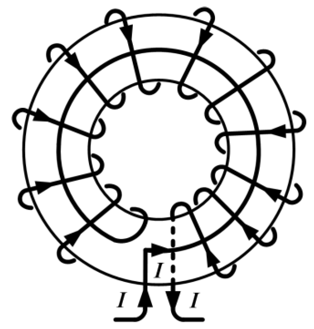
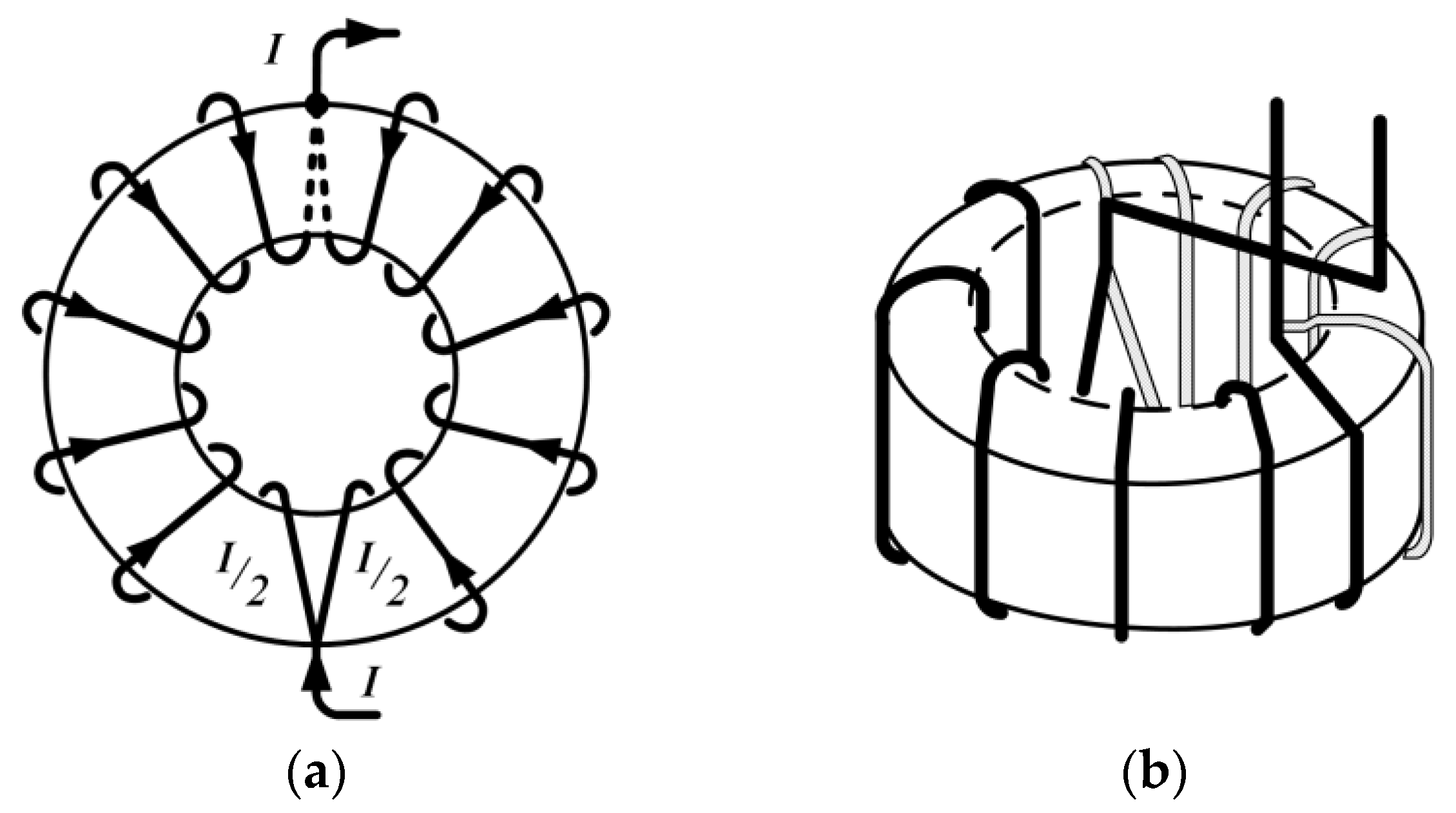
2. Proposed Compensation of External Magnetic Fields

Inductors with toroid cores are negligibly influenced by external magnetic fields compared to solenoid inductors. There are two established methods for further suppression of its influence (and to further decrease the magnetic field generated by the inductor): the first method uses compensation with an additional single turn (Figure 1), while the second method (Figure 2) applies duplex winding [6,7,24]. Compared to them, plane inductors made using PCB technology suffer from greater influence from the external fields, similar to inductors with solenoid cores. To minimize this influence, we propose a planar duplex system, with two equal spiral PCB inductors. The concept is depicted with two circular loops in Figure 3.
The currents in loops depicted in Figure 3 can be arranged in two ways: with magnetic fluxes supporting (a) and subtracting (b). In a usual solenoid inductor, the individual turns to produce supporting axial magnetic fluxes.
A single circular loop can be for large distances ( r r ) approximated as a magnetic dipole with a magnetic moment m = n 0 I S , where I denotes the electric current, S is the area of the loop, and n 0 is the unit normal vector (Figure 4). The scalar magnetic potential and associated magnetic flux density are [23] (p. 179):
Φ = m · r 4 π r 3
B = μ Φ
In the proposed planar duplex system of loops (arranged as an anti-Helmholtz pair), with currents flowing in opposite directions, at large distances, the total magnetic scalar potential vanishes since the magnetic dipole moments of two loops are opposite one another. Consequently, the magnetic flux density vanishes too. In addition, if such a planar duplex system is exposed to an external time-varying homogenous magnetic field B e x t , the induced voltages v e x t will have the same magnitude in both loops, thus leading to cancelation (Figure 5). Note that the loops are connected in series, while in traditional toroidal duplex windings, the coils are paralleled. In a non-homogenous magnetic field, cancelation will also occur, albeit imperfectly, if the distance between loops is small compared to their radius.
The external inductance of a single circular loop (Figure 6a) is equal to [25,26]:
L v = µ r 0 + r [ r 0 2 + r 2 r 0 + r 2 K k E ( k ) ] ,   k = 2 ( r 0 r ) 1 / 2 r 0 + r
where µ denotes magnetic permeability, K(.) is the complete elliptic integral of the first kind, and E(.) is the complete elliptic integral of the second kind. The inner inductance is:
L u = µ 4 π 2 π r 0 = 1 2 µ r 0 ,
yielding the self-inductance of the loop as L = L u + L v .   For R r 0 , the self-inductance of the loop is approximately:
L = L u + L v = µ r 0 [ ln 8 r 0 R 3 2 ]
Mutual inductance of the system (Figure 6b) can be determined as [26]:
L 12 = 2 µ ( r 1 r 2 ) 1 2 k 1 1 2 k 2 K k E k ,   k 2 = 4 r 1 r 2 ( r 1 + r 2 ) 2 + z 12 2
If k is close to 1, an approximate formula for mutual inductance is:
L 12 = µ ( r 1 r 2 ) 1 2 k l n 4 k 2 ,   k 2 = ( r 1 r 2 ) 2 + z 12 2 ( r 1 + r 2 ) 2 + z 12 2 = ϱ 0 2 4 r 1 r 2 + ϱ 0 2
Analytical formulas for the self- and mutual inductances of planar spiral and rectangular coils can be found in [27,28,29,30,31,32]. Self- and mutual inductances of a system of two multi-turn coils can also be calculated using software for numerical electromagnetic analysis, like finite element analysis (FEA). The equivalent inductance of two loops connected in series, if their magnetic fluxes are subtracting, is:
L e q = 2 L L 12
Here, L 12 < L will always be satisfied for each two inductors with equal inductance [25]. In this way, with two identical loops connected in series in the anti-Helmholtz configuration (or planar duplex configuration), an inductor can be designed with significantly reduced sensitivity to external magnetic fields. The same combination will also generate significantly lower magnetic fields compared to a single planar loop or a wound inductor with a solenoid core. Moreover, by adjusting the distance z 12   between coils, the equivalent inductance of the system can be precisely adjusted during manufacturing. Considering parasite capacitances and resistances, as well as self- and mutual inductances, the equivalent circuit diagram of the planar duplex system of two loops is depicted in Figure 7, which is similar to the equivalent diagram of two adjacent circular rings in transformer windings [33]. The presented concept of two circular loops can be extended to a pair of multi-turn planar spiral coils (circular or rectangular) to achieve higher inductances of the system.

3. Design of the System

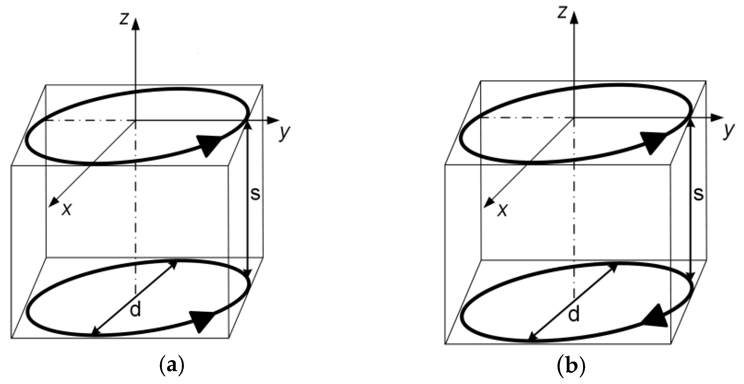
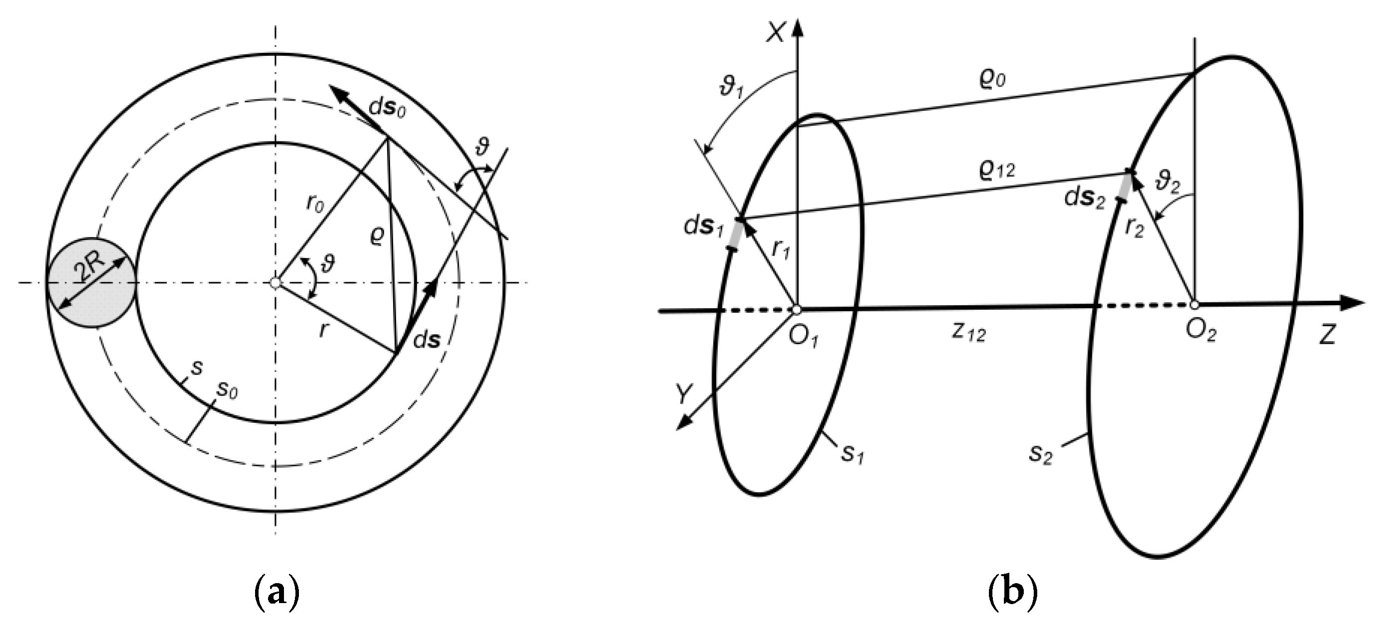
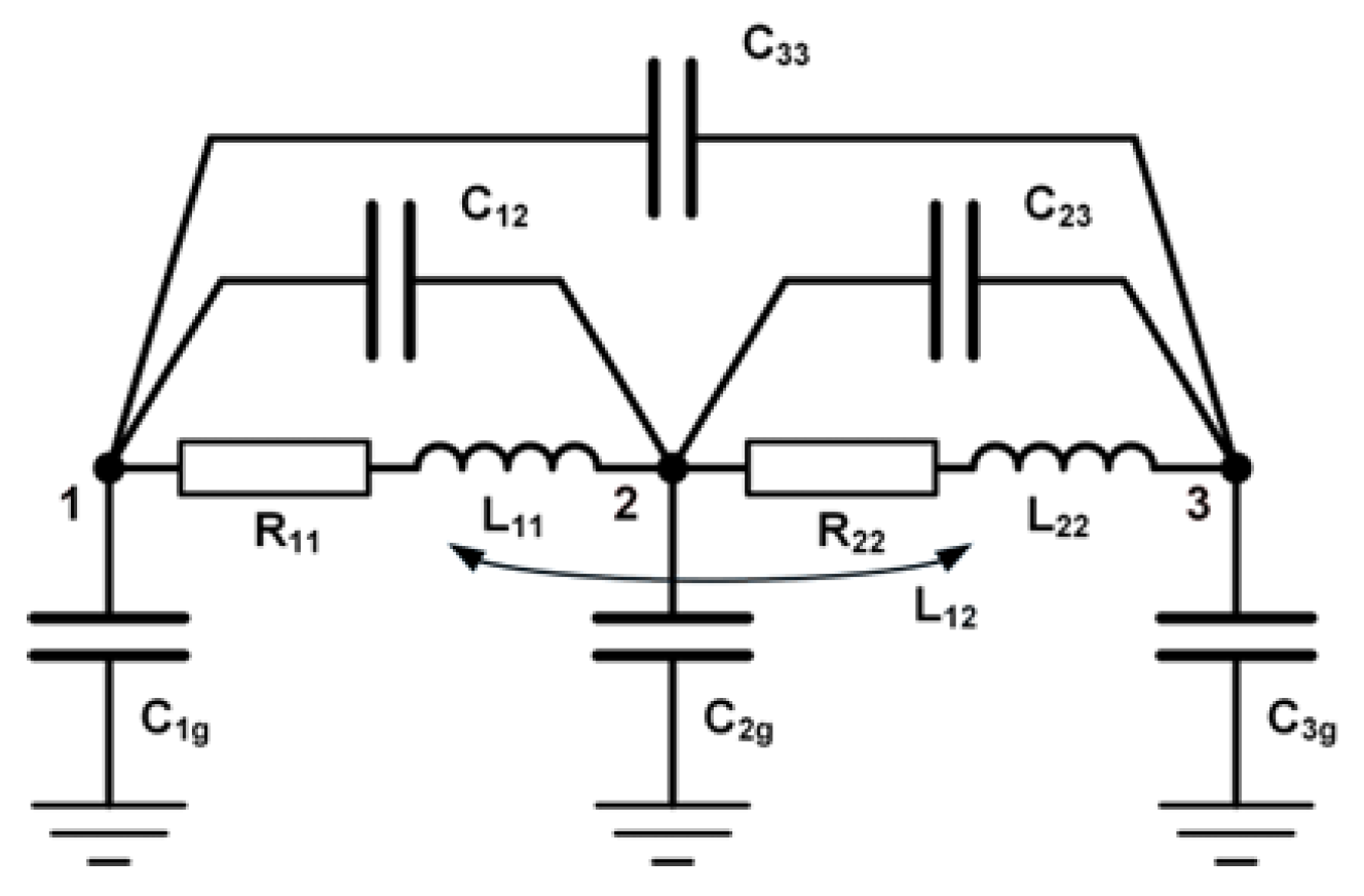
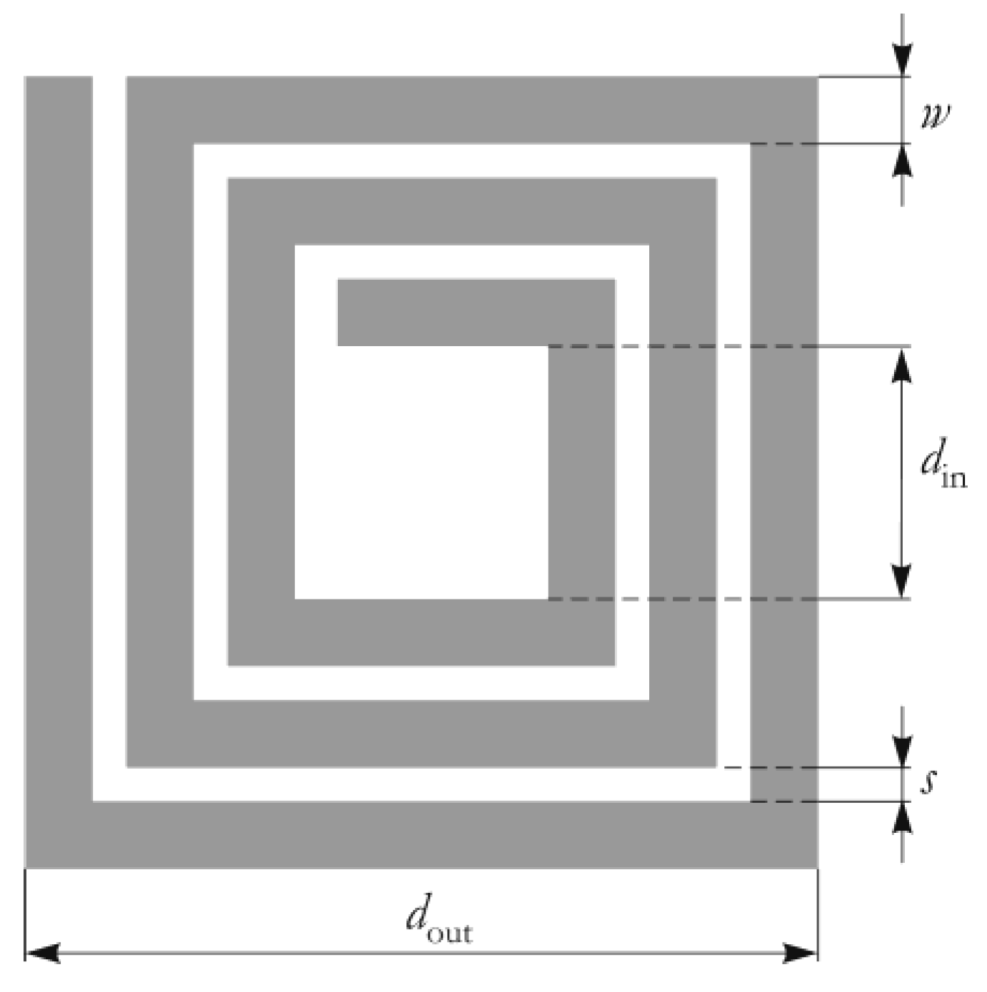
3.1. Inductance of a Spiral Rectangular Coil

The inductance of the printed planar inductors can be estimated using several analytical expressions. Figure 8 depicts the square realization of the planar inductor. The planar inductor is specified by the number of turns n, the turn width w, the turn spacing s, the outer diameter dout, and the inner diameter din. Furthermore, the average diameter d a v g = 0.5 ( d o u t + d i n ) , and the fill ratio is ρ = ( d o u t d i n ) / ( d o u t + d i n ) .
Based on the work of Mohan et al. [27], the modified Wheeler formula for the inductance of the square realization of the spiral inductor is:
L m w = 2.34 µ 0 n 2 d a v g 1 + 2.75 ρ
There is also an expression based on current sheet approximation and mean distances [27]:
L g m d = 1.27 µ 0 n 2 d a v g 2 [ ln 2.07 / ρ + 0.18 ρ + 0.13 ρ 2 ]

3.2. FEM Calculations

The design procedure started from the nominal inductance of 10 μH for each spiral PCB coil, setting the trace thickness (35 μm), trace width (1 mm), the space width between traces (1 mm), and inner diameter din (Figure 8).
Using the Wheeler formula, i.e., Equation (9), the initial number of turns N was calculated, where N = 18 gave a slightly lower value, while N = 19 gave a slightly greater value than nominal. After that, a finite element method (FEM) model with 19 turns was created in Ansys Maxwell 2024 R1 (24.1) software, and the space between the last two turns was increased in steps of 0.5 mm to more finely adjust the inductance closer to the desired value. Table 1 summarizes the results, and Figure 9 presents the final design of the PCB inductor, containing 19 turns and space between the last two turns equal to 2 mm. The PCB was manufactured in standard FR-4 laminate. The thickness of the laminate was 1.6 mm to assure mechanical stability and stiffness.
Using the FEM model of a two-coil system (Figure 10), the distance between the coils was calculated to determine the nominal inductance of the system. Table 2 gives the inductances for 4 different distances, which correspond to the equivalent inductance of the system in the vicinity of the nominal value of 10 µH. The two nearest points to the nominal value (8.5 mm and 15 mm) were used in linear interpolation to determine the distance used in the manufacturing of brass spacers. The fine-tuning of the inductance was performed experimentally during assembly, using additional washers and fine machining of the spacers. The entire system was positioned in the middle of a cubic aluminum case (air bath), which ensures electrostatic shielding.

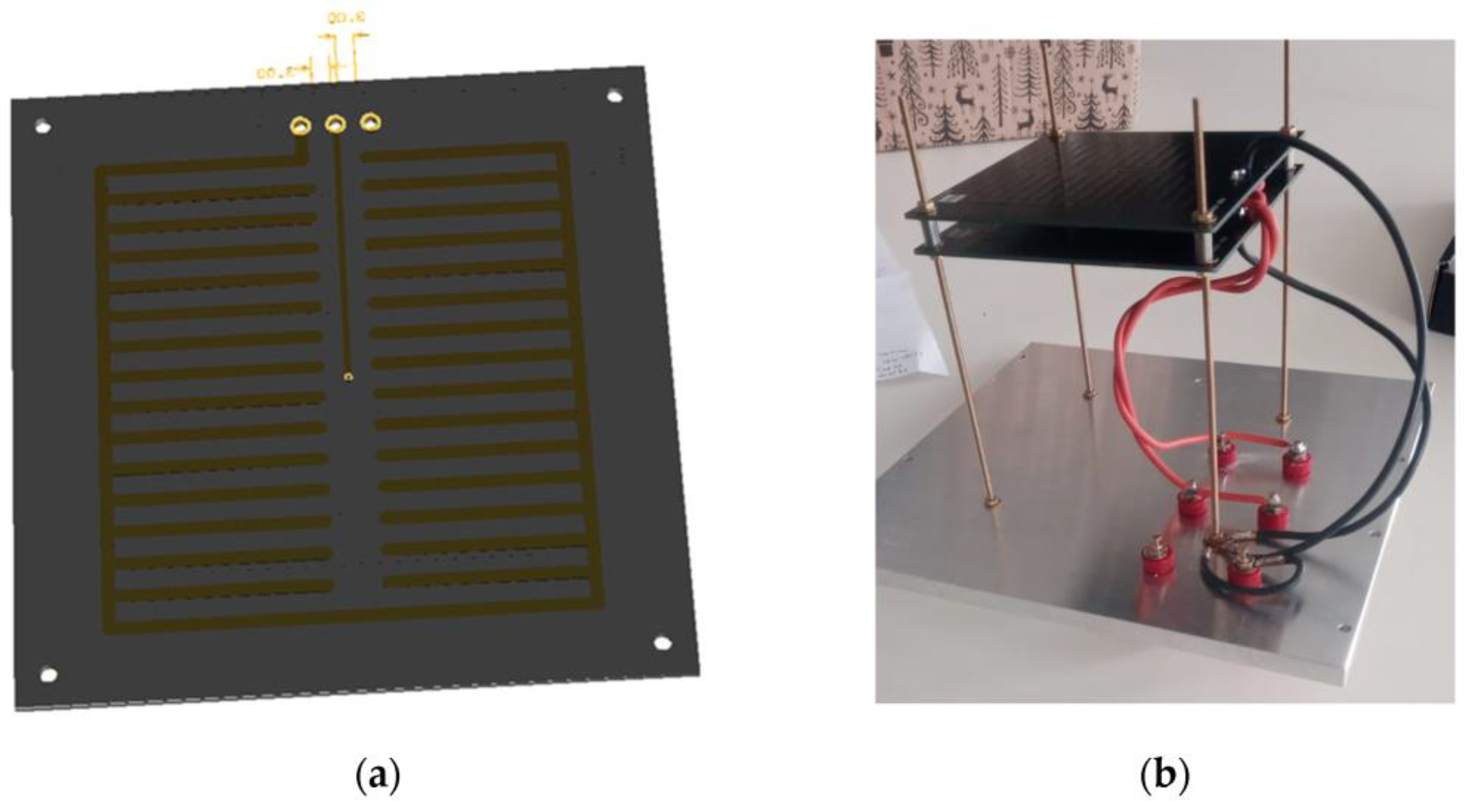
3.3. Enclosure and Electrostatic Shielding

Inductors not contained within a conducting box have a capacitance to their surroundings [24] (p. 84). Enclosing the inductor within the conductive shielding also eliminates external electric fields [24] (p. 86). To further enhance shielding against electric fields and make all capacitances well-defined, additional shielding in the form of a comb-shaped copper shielding on the reverse side of the PCB is added (Figure 9, blue trace). Comb-shaped shielding (Figure 11a) was applied as electrostatic shielding in [34,35], while a similar type of shielding against electric fields was also implemented in PCB magnetic field probes [18,19,20,21,22]. The star grounding of the system was ensured connecting all PCB shields and the enclosure to the “ground” binding post (Figure 11b), using individual conductors for each shield. All connectors were red binding posts with tellurium copper contacts and gold plated (Mueller Electric 15A, Mfr. Part No.: BU-P3770-2) to assure their low impedance and low thermal emf. The inductance standard is equipped with two connection terminals, and three shorting terminals (Figure 12a) in an arrangement typical for inductance standards with low nominal inductances [6]. This allows for shorting the inductor using the external ground strap or connecting the ground strap in series with the inductor and consequently allows for measurement of the cable inductance and resistance in bridge measurements without disconnecting the inductor. Temporarily, instead of the external ground strap, a wire is soldered between the terminals, thus allowing for DC resistance measurement using a 4-wire connection. Within the enclosure, two PT100 temperature probes, (class A) (Keysight, 34152A), were mounted. One of them was mounted laterally on the upper panel, while the second was positioned freely in the air, in the middle of the enclosure, with the aim of monitoring the temperature and determining the time constant of the enclosure. A hole was drilled in the front panel for wire contacts of the temperature probes and sealed after assembly of the system to reduce its influence on the heat transfer to the interior of the enclosure.
Magnetic flux density in the vicinity of the inductance standard was measured using a shielded magnetic field pick-up coil (Rohde & Schwarz, HZ-10 and a spectrum analyzer (Keysight, N9332C) at several positions in the vicinity of the enclosure. The distance between the enclosure and the pick-up coil was 7 cm, using the spacing plate supplied with the coil. Figure 12b depicts the position of the maximum measured magnetic flux density. Besides the position presented in Figure 12b, the pick-up coil was positioned symmetrically at the edge of the enclosure, with its plane forming an angle of 45 degrees with the sides of the enclosure. Finally, the enclosure was rotated vertically at 90 degrees, and measurements were repeated in the same positions. During measurements, the current through the inductor was set to approximately 50 mA, corresponding to a dissipation of 5 mW in the inductor, which was estimated to cause negligible change in the resistance and inductance of the standard. The current was generated using a a function generator (GW Instek, AFG-2005) and a protective resistor (Vishay) with a nominal value of 50 Ω mounted in a shielded box, connected in series with the inductor. The magnetic flux density was measured for frequencies 10 kHz and 100 kHz. To prevent additional current loops associated with direct measurement of the current using a digital multimeter (DMM), the current was measured indirectly, using the voltage of the inductor (measured using a digital multimeter) (Keysight, 34465A) and its impedance, measured using an LCR meter (Keysight, E4980AL). For 10 kHz, the measured maximum magnetic flux density was 1.68 nT, where the current was 48.86 mA. The limit error for the current measurement was 0.17 mA, using data supplied by the manufacturers. The corresponding input signal level on the spectrum analyzer was −75.77 dBm, which is below the lowest signal level (−50 dBm) with accuracy data supplied by the manufacturer. As a comparison, a signal level of −50 dBm would be produced with the same pick-up coil at a magnetic field density of 32.70 nT. For that magnetic field density, the type-B uncertainty of magnetic flux density measurement would be 4.68 nT (k = 1), using data supplied by Keysight and the calibration certificate of the pick-up coil. For 100 kHz, the maximum measured magnetic flux density was 1.47 nT, again below −50 dBm. The measured current was 50.15 mA, with a limit error of 0.75 mA. At a frequency of 100 kHz, a signal level of −50 dBm would be produced at a magnetic field density of 12.57 nT, with associated type-B uncertainty of 2.12 nT (k = 1). The resonant frequency of the inductor standard was measured using a vector network analyzer (VNA) (Keysight, E5061B) and a calibration kit (Keysight, 85033E). An adapter consisting of two short litz wires soldered to an SMA connector (f) was made to enable connection of the RF cable to the binding posts. The resonant frequency was calculated from the phase angle of reflection coefficient s 11 , using linear interpolation between measured samples to find the frequency of phase angle zero. The measured resonant frequency of the standard was 7.66 MHz. Corresponding magnitudes of s 11 (>0.9) are in the region where its phase angle measurement introduces inaccuracies generally less than 2 ° [36], although the VNA data sheet does not specify accuracies with any SMA calibration kit applied, including 85033E. Problems and methods arising with accurate device radio frequency (RF) characterization using scattering parameters are discussed in [37,38]. Assuming a maximum phase angle error of reflection coefficient equal to 2 ° , the limits of resonant frequency lie in the frequency region between 7.14 MHz and 8.18 MHz. Since the inductor standard is a low-frequency device, it is all well above its operational frequency range and very similar to the typical resonant frequency of a General Radio 1482-AA inductance standard (7.5 MHz).

4. Temperature Coefficients—Materials and Methods

Within the scope of this research, the thermal time constant and temperature coefficient of resistance (TCR) of the inductance standard were determined. Also, the influence of temperature on inductance was examined. The characterization of the inductance standard was performed in the temperature range of 10 °C to 40 °C. All measurements were conducted in the Laboratory for Process Measurement (LPM) within the Faculty of Mechanical Engineering and Naval Architecture at the University of Zagreb. This laboratory maintains the Croatian national standard for temperature, pressure, and humidity, ensuring that all temperature measuring equipment used is directly traceable to the primary temperature standard [39]. Traceability was ensured using a thermostatic calibration bath (Kambič, OB-15/2) filled with water and a standard platinum resistance thermometer (Hart Scientific, 5628) connected to a precision thermometry bridge (Isotech, ASL F18). The standard thermometer was primarily characterized via calibration at fixed points in LPM with an uncertainty of less than 5 mK, while the traceability of the ASL F18 was achieved through the calibration of fixed resistors.

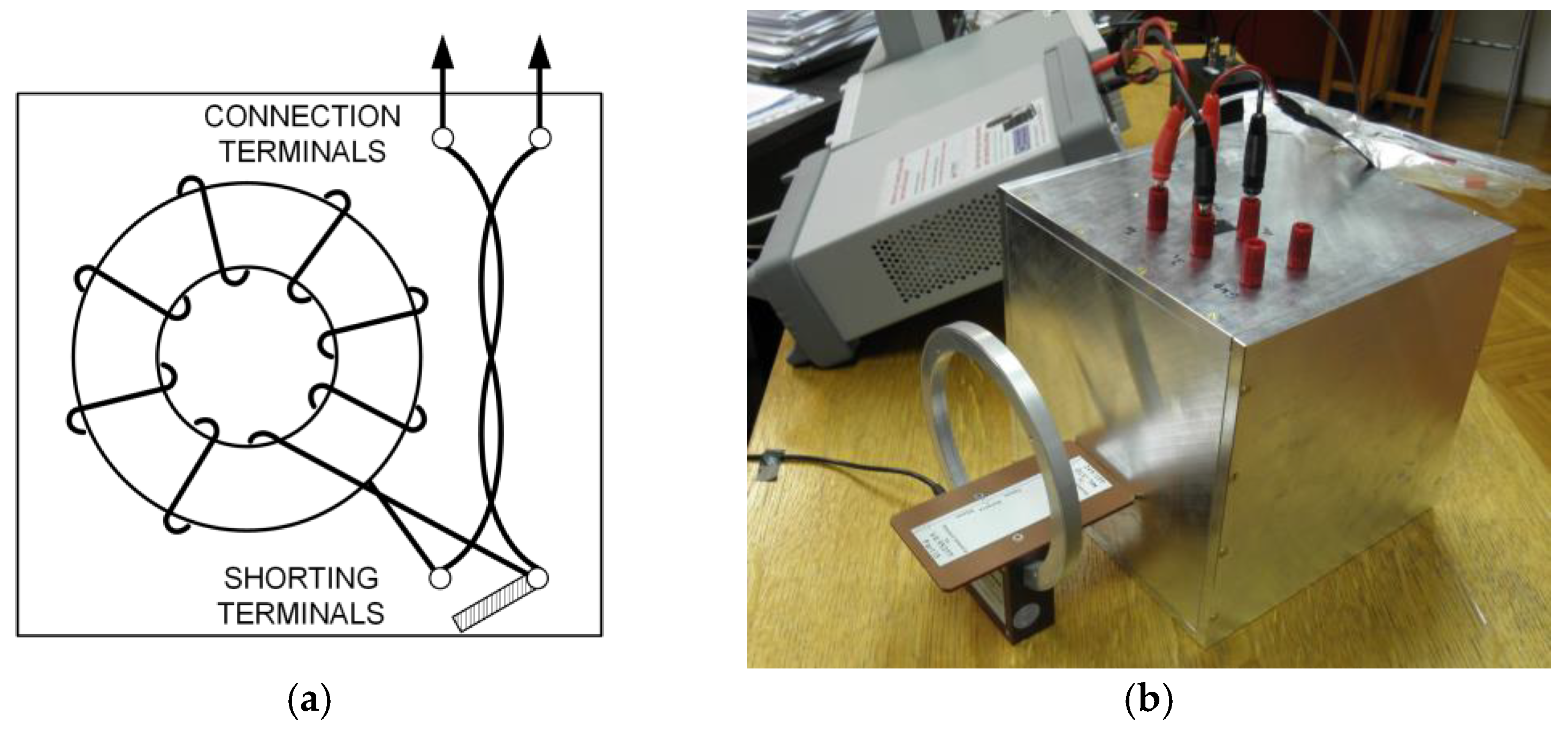
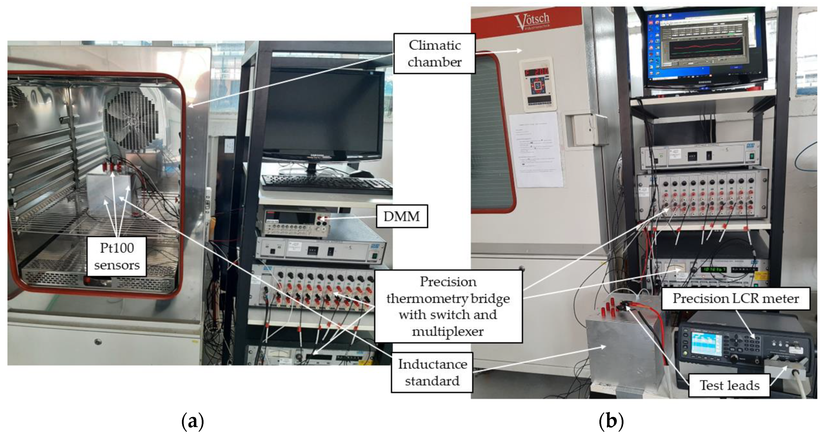
4.1. Measurement Setup

The thermal characterization of the inductance standard was performed using a climatic chamber for the simulation of different thermal conditions for the inductance standard. The measurement setup can be seen in Figure 13. The inductance standard was placed in the middle of the working volume of the climatic chamber (Vötsch, VC-0033). During the determination of the thermal time constant, the temperature was measured with eight Pt100 probes connected to a precision thermometry AC resistance bridge (Isotech, ASL F700) via a multi-channel switchbox (Isotech, ASL SB148/01) and interface (Isotech, ASL SB158). All Pt100 probes were previously calibrated, and their uncertainties were determined to be 30 mK. Two measuring probes were placed inside the standard and six were placed outside the housing of the standard, one at each panel. The determination of the temperature coefficient of resistance was performed using the same setup, with an additional digital multimeter (Keithley, 2010) for DC measurement of resistance. The inductance and ac series resistance at different temperatures were measured using a precision LCR meter (Keysight, E4980AL) with Kelvin test leads (Keysight, 16089B-C20). The LCR meter was commercially calibrated at Keysight Servicezentrum (Böblingen, Germany) accredited by the United Kingdom Accreditation Service (UKAS) on a yearly basis.

4.2. Determination of the Temperature Coefficient of Resistance (TCR)

For the determination of the temperature coefficient of resistance (TCR), the DC resistance of the inductance standard was measured in the temperature range of 10 °C to 40 °C with a 5 °C interval between measuring points. After the detection of the thermal stabilization of the chamber and inductance standard, the 4-wire DC resistance was measured with compensation of the thermal voltage offset across the inductance standard (“Offset compensation” mode). The interchange of the connecting leads was performed between two measurements to account for their influence. Hysteresis was determined with repeated measurements at 20 °C and 35 °C. The measurement uncertainty analysis of the measured resistance included the influence of temperature measuring equipment, the DMM, the inductance standard, and the temperature inhomogeneity of the climatic chamber.

4.3. Determination of Thermal Time Constant

The thermal time constant (τ) of the inductance standard is the time required for the standard to reach 63.2% of its final (asymptotic) temperature after a step change in its ambient temperature. A step change in the ambient temperature was achieved by inserting the inductance standard in the preconditioned chamber from the ambient temperature or by removing the thermally stabilized inductance standard from the chamber to the ambient laboratory environment.
The determination of T was conducted with two methods. In the first method, the initial ( ϑ 0 ) and final (asymptotic) temperature ( ϑ ) were detected from the measurement data. From Equation (11), the temperature when ϑ t = τ was calculated. The exact time when the inductance standard reached this temperature, was then interpolated from the closest two measured data points.
ϑ t = ϑ + ( ϑ 0 ϑ ) · e t τ ,
The second method was the least-squares method that involved fitting the measured data into Equation (11) and finding the τ that resulted in the smallest difference between the measured and fitted data, using the Microsoft Excel Solver add-on.

4.4. Measurement of Inductance

The series inductance L S   and series resistance R S were also measured at seven temperature points in the range of 10 °C to 40 °C with 5 °C intervals. Before measurement at each temperature point, the inductance standard was left in the chamber for thermal stabilization. After reaching the required stability, the standard was taken out of the chamber and connected to the precision LCR meter via specialized test leads, and the measurement sequence at three frequencies (10 kHz, 50 kHz, and 100 kHz) was completed within 30 s, to avoid the significant temperature drop. Also, prior to the commencement of the measurements, compensation of the test leads was performed. Hysteresis was determined by repeating the measurements at 20 °C. The low-frequency equivalent circuit of an inductor is a simple series circuit consisting of an ideal resistor and an ideal inductor. At high frequencies, the more accurate representation includes the lumped parameter approximation of the stray capacitance between turns of the inductor (Figure 14) [1,6]. Starting from the equivalent lumped parameter model of the inductor (Figure 14) [1,6] we define series inductance L S and series resistance R S using its equivalent impedance Z L j ω :
Z L j ω = R S + j ω L S = R 1 ω 2 L C + ω R C 2 + j ω L [ 1 ω 2 L C ( C R 2 / L ) ] 1 ω 2 L C + ω R C 2
where ω denotes the angular frequency. It is noteworthy that measurement of L S and R S over a wide range of frequencies (using an LCR meter) generally gives frequency-dependent series inductance and resistance. Nevertheless, at low frequencies, the influence of C is negligible, and Equation (12) simplifies to Z L j ω = R + j ω L .

5. Results

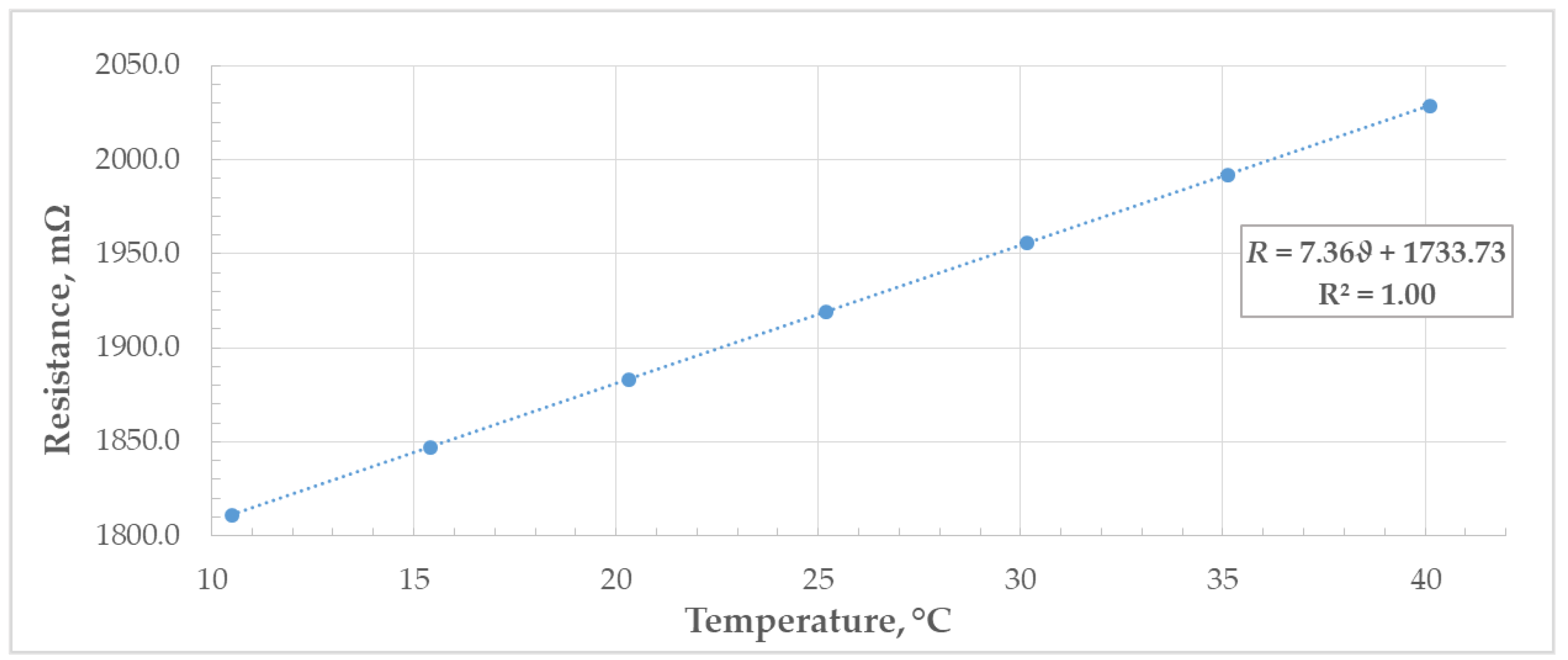
5.1. Temperature Coefficient of Resistance

The results of the determination of the temperature coefficient of resistance can be seen in Table 3 and Figure 15. An increase in temperature leads to a linear increase in resistance. Measurement uncertainty analysis considers the combined influence of temperature measurement equipment and the climatic chamber; and the influence due to the characteristics of the DMM and the inductance standard, with the thermal inhomogeneity of the chamber as the largest contributing factor. The uncertainty of the measured DC resistance increases toward the upper and lower limit of the temperature range, which corresponds to larger spatial temperature gradients and temporal instability in the climatic chamber at those temperatures. This is especially significant at 10 °C, which is the lower temperature limit of the chamber.
The temperature coefficient of resistance [1] is defined as:
α = d R ( T ) / d T R ( T )
where T denotes the reference temperature. Using linear regression from Figure 15, we obtain the temperature coefficient of resistance equaling 0.00384   1 at the reference temperature 25   .

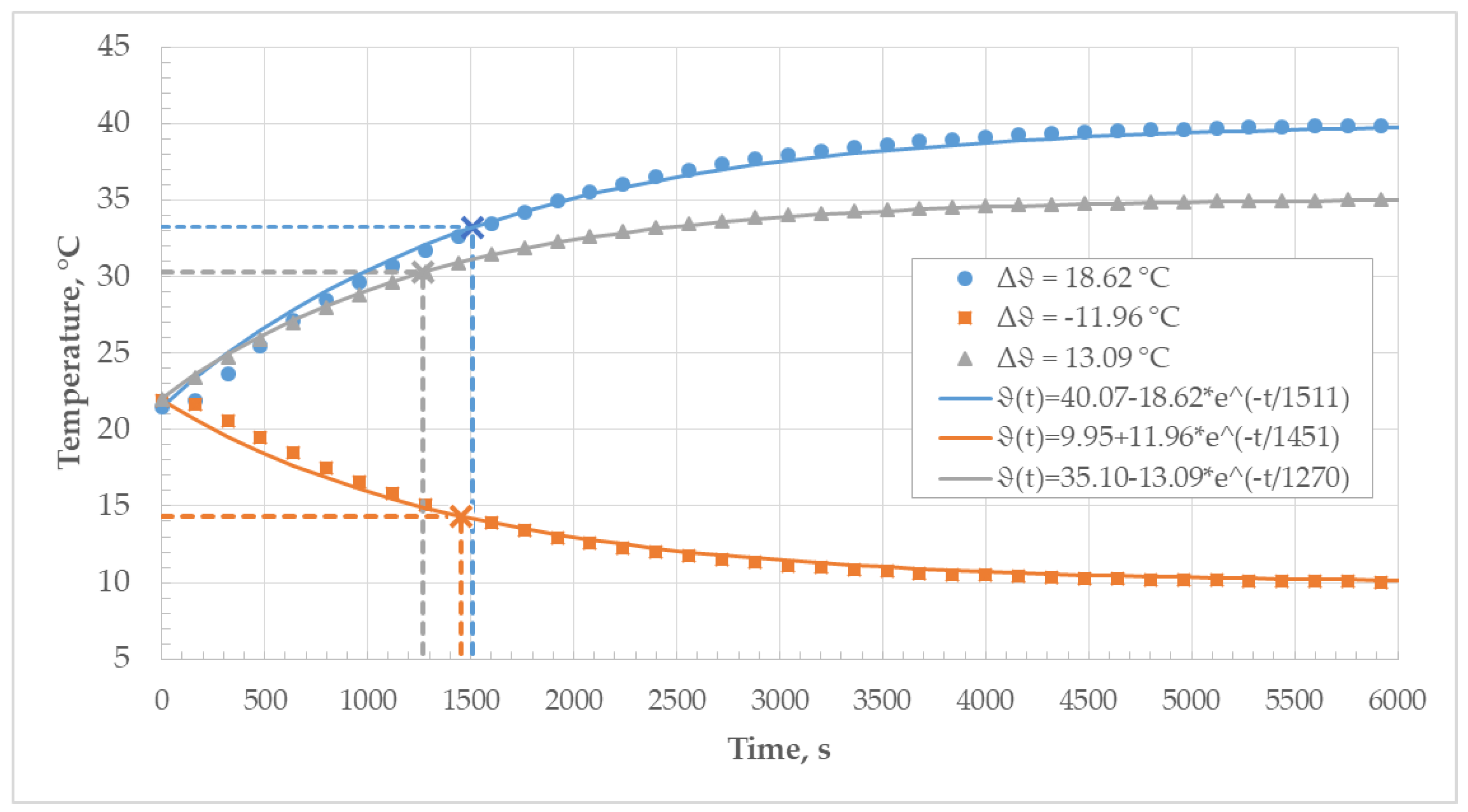
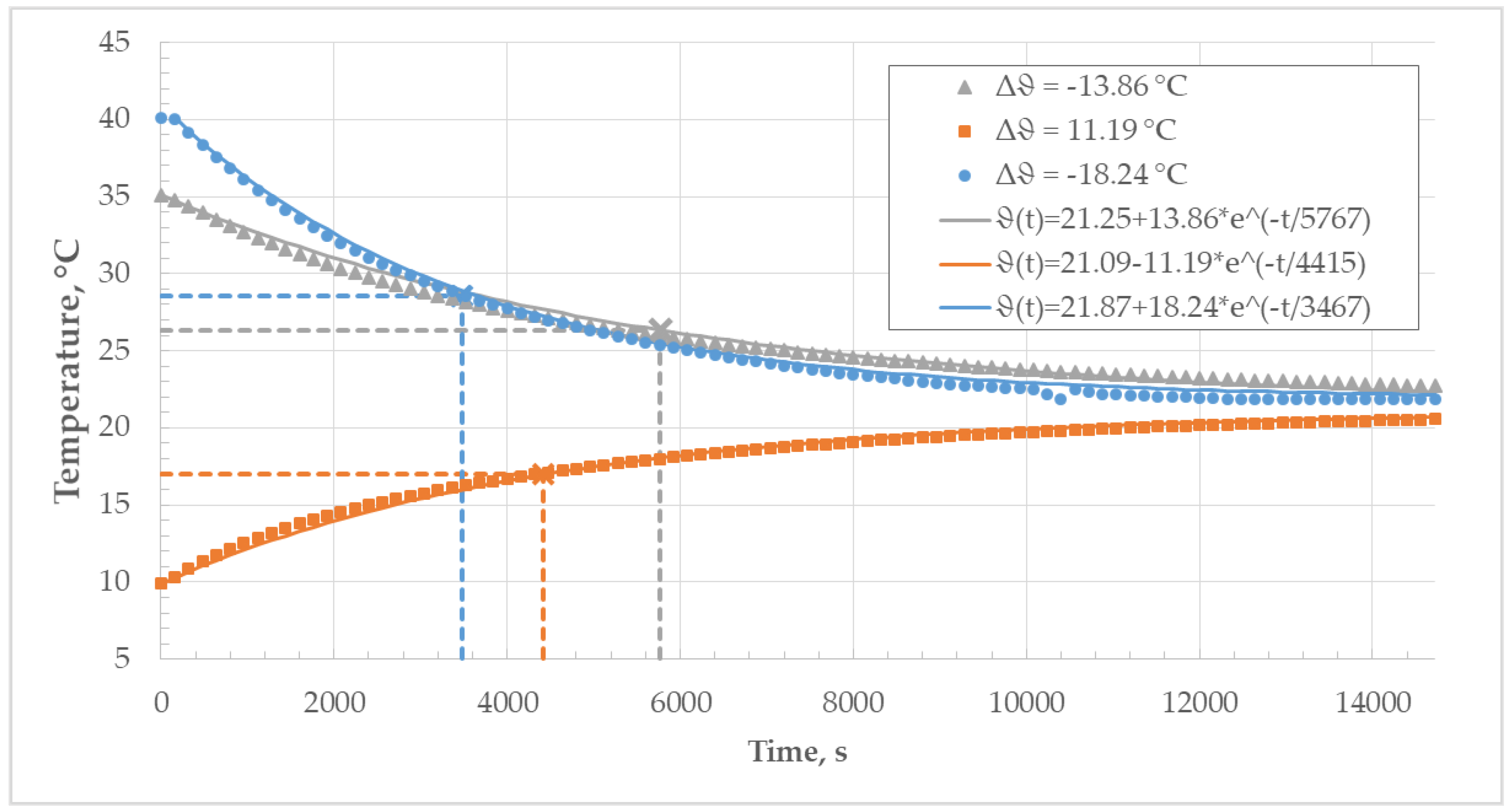
5.2. Determination of Thermal Time Constant τ

The determination of the thermal time constant was divided into two parts since there were two environments for thermal stabilization after the temperature step change in the inductance standards with different characteristics. Figure 16 shows the thermal behavior of the inductance standard after the step change in its ambient temperature, from laboratory ambient air to a stable thermal environment inside the climatic chamber.
The thermal time constant was determined for every temperature difference using the two methods. The results can be seen in Table 4. The agreement between the results obtained with both methods is within 3%.
When the thermally stabilized inductance standard in the chamber was exposed to the ambient air temperature in the laboratory, significantly larger time constants were determined, as can be seen in Table 5 and Figure 17. This can be attributed to the fact that the heat exchange between the standard and the ambient air in this case is mostly governed by natural convection in comparison to the forced convection in the chamber due to the circulation of air caused by the fan.
Since the behavior of the ambient air in the laboratory cannot be strictly controlled, thermal time constants for different temperature step changes differ significantly in comparison to the ones obtained with step changes induced by insertion into the climatic chamber. The differences between the time constants determined using the two methods are slightly higher in this case but do not exceed 9%.

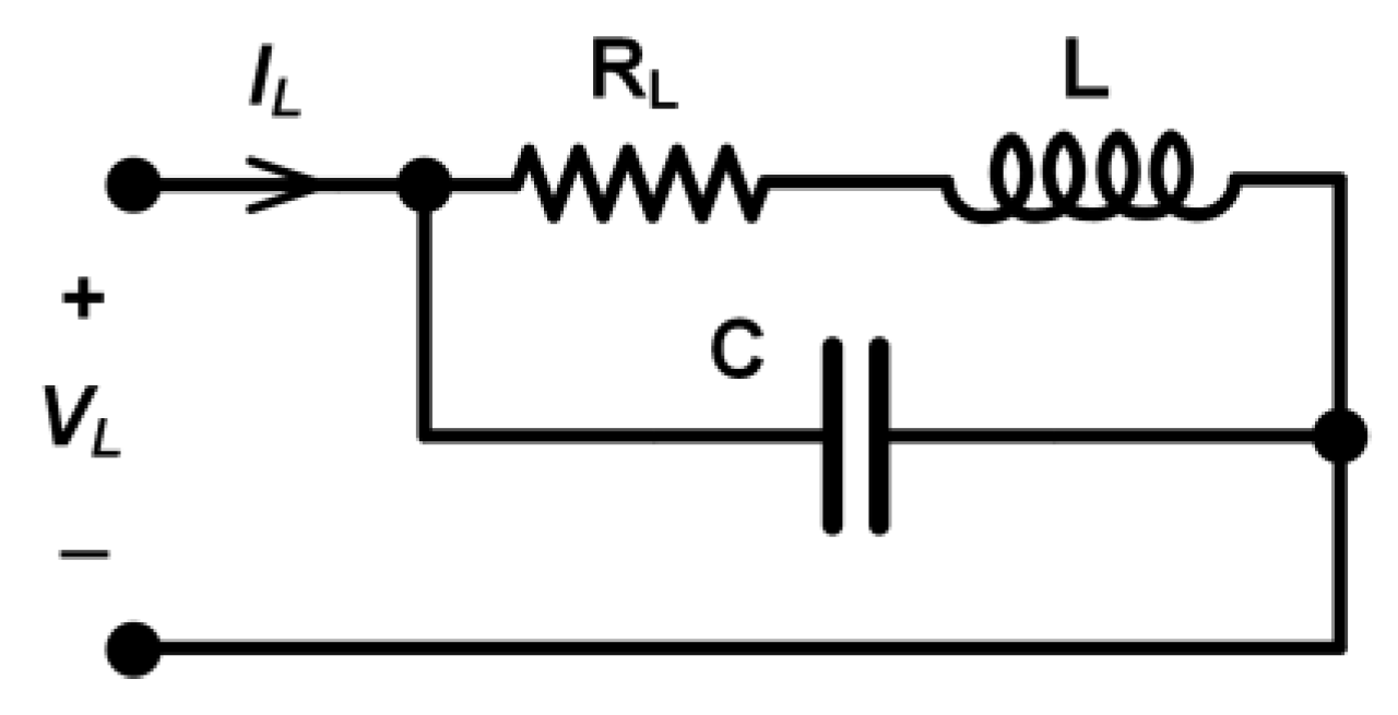
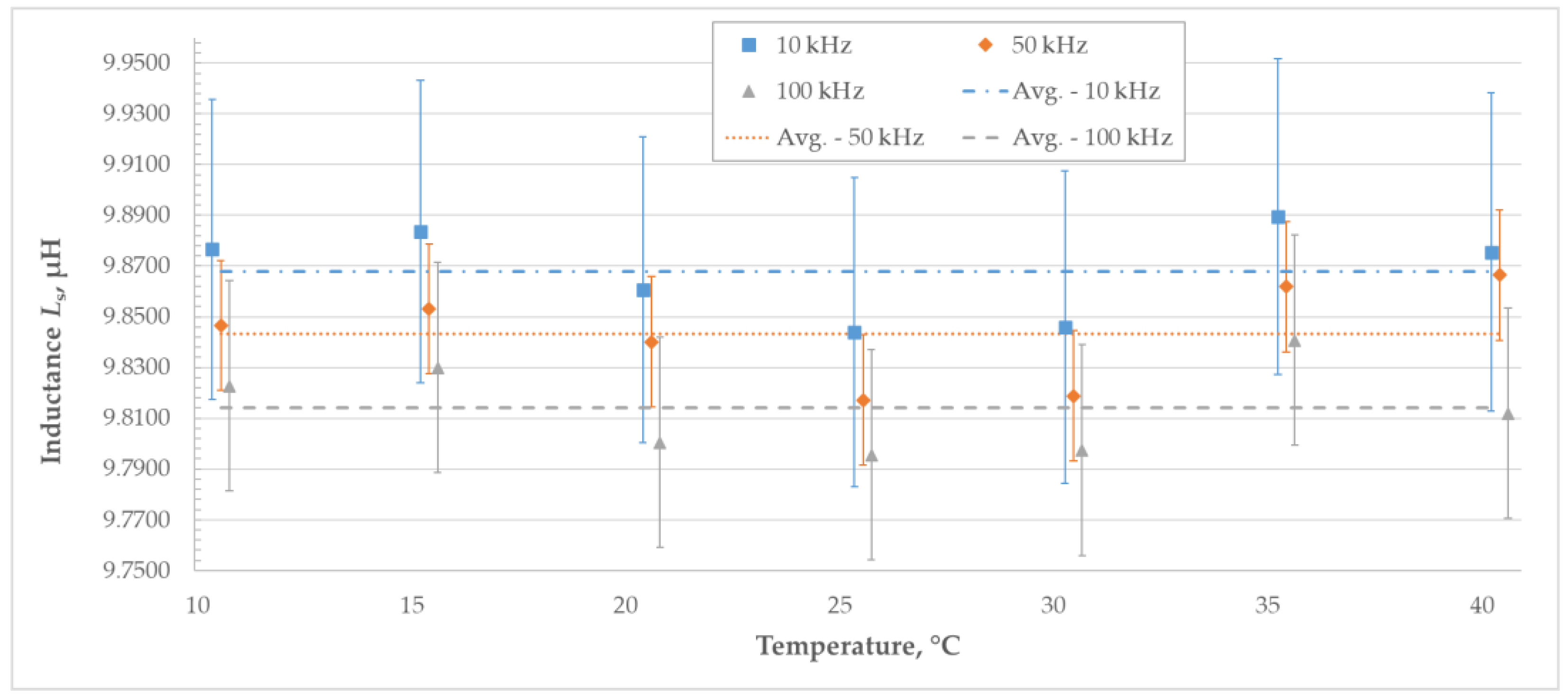
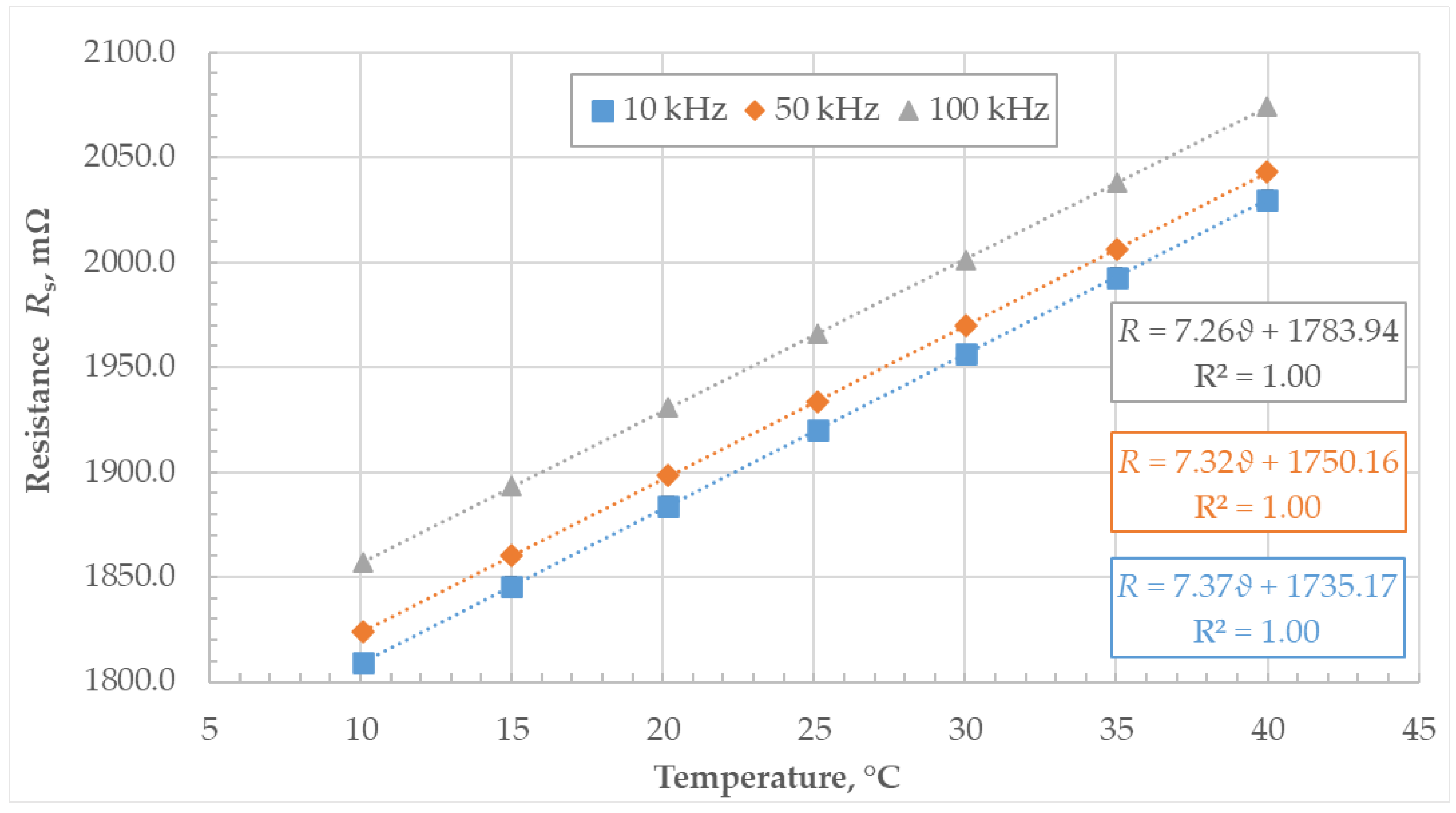
5.3. Measurement of Series Inductance and Series AC Resistance

Results of the measurements of series inductance with the LCR meter are shown in Figure 18 and Table 6. Inductance measured at all three frequencies follows the same trend with values lower than average in the temperature range of 20 °C to 30 °C, as can be seen in Figure 18. At higher frequencies, the measured series inductance is lower. The dependence of the measured series inductance on temperature together with associated uncertainties is shown in Figure 18.
Measurement uncertainty of the series inductance stated in Table 6 and graphically presented in Figure 18 includes the influence of the standard deviation of the measured results, LCR meter accuracy, and hysteresis.
The series resistance measured with the LCR meter exhibits higher values at higher frequencies, as can be seen in Figure 19 and Table 7. The temperature dependence of the measured series resistance agrees with the values obtained during measurements with the DMM, showing a positive linear increase in resistance with temperature.
The measurement uncertainty stated in Table 7 takes into account the influence of the LCR meter, the standard deviation of the measured resistance, and hysteresis.

6. Discussion and Conclusions

The proposed design encompasses the ease of manufacturing and low cost of PCB inductors with low levels of generated magnetic flux densities in the vicinity of the inductor enclosure. The thermal time constant of the enclosure varies with the environment. In the laboratory environment (with the natural convention), it does not exceed 3467 s, while in the climatic chamber (forced convection), it does not exceed 1270 s. Such a relatively long thermal time constant of the enclosure ensures that temporary changes in the environmental temperature will affect the temperature of the inductor to a lesser degree during its operation, while the electrostatic shielding of the inductor ensures that all capacitances are well defined. Furthermore, the thermal time constant of the enclosure is long enough to allow the standard to be taken out of the climatic chamber after reaching thermal stabilization, thus simplifying the measurement campaign for the determination of the thermal coefficient of inductance and AC series resistance. The measured DC resistance and AC series resistance show the expected linear trend. For DC resistance, the slope of linear regression is 7.36   m Ω / , with a corresponding temperature constant of resistance equaling 0.00384   1 at 25   . This parameter can be applied for indirect estimation and monitoring of the inductor temperature during its operation. The temperature dependence of AC series resistance measured with the LCR meter exhibits linear trends for all frequencies, with expected higher resistances associated with higher frequencies due to the proximity and skin effects. At the lowest frequency (10 kHz), where the impedance has a dominantly resistive character (thus reducing the measurement error of the series resistance relatively), the temperature coefficient of resistance equals 0.00384   1   at 25   , the same as the DC resistance. Regarding the temperature coefficient of the series inductance, inductance measured at all three frequencies follows the same trend, with values lower than average in the temperature range from 20 °C to 30 °C. L s also shows a decrease with frequency for the three applied frequencies (i.e., 10 kHz, 50 kHz, and 100 kHz), which can be also attributed to the proximity and skin effects [11]. With further increases in frequency in the MHz range, L s   exhibits an increase with frequency, which is in line with the lumped-parameter model of the real inductor with constant inductance, resistance and capacitance. In the temperature range spanning from 10.11 to 39.98 and for a frequency of 50 kHz, the minimum measured inductance was 9.82 µH and the maximum measured inductance was 9.87 µH, while uncertainty was 0.03 µH (k = 2). Thus, the difference between minimum and maximum inductance is 0.05 µH, which is very close to uncertainty in inductance measurements. A similar ratio between minimum and maximum measured inductance and corresponding uncertainty is visible for the other two frequencies. To investigate a possible hidden linear trend, the linear regression was calculated for all three frequencies, using the entire temperature range from 10.11 to 39.98 . The calculated temperature coefficients of the inductances using linear regression were scattering as −5.1 µH/H/ (at 10 kHz), 40.6 µH/H/ (at 50 kHz), and −10.2 µH/H/ (at 100 kHz). More consistent results would be expected with more precise measurement of inductance, which is planned in the future as well as the monitoring of the long-term drift. The PCB inductors were manufactured using a standard trace thickness of 35 μm, resulting in the DC resistance of the inductor being equal to approximately 1.8 Ω. The connection of two PCB inductors in series, which reduces the magnetic field in the surroundings and the sensitivity of the inductor to external magnetic fields, also doubles the resistance (compared to a single PCB inductor). The future re-design will include thicker copper traces, which will decrease resistance, reduce power losses, and increase the resonant frequency. With reduced resistance, the same temperature rise and corresponding heating effects on the parameters of the inductor would occur at higher currents.

Author Contributions

Conceptualization, Ž.M., M.D., I.M. and L.G.B.; methodology, Ž.M., M.D., I.M. and L.G.B.; software, Ž.M. and I.M.; validation Ž.M., M.D., I.M. and L.G.B.; formal analysis Ž.M., M.D., I.M. and L.G.B.; investigation, Ž.M., M.D. and I.M.; resources, M.D. and L.G.B.; visualization, Ž.M. and I.M.; supervision M.D. and L.G.B.; project administration, M.D.; funding acquisition, M.D. All authors have read and agreed to the published version of the manuscript.

Funding

This research is supported in part by the Croatian Science Foundation under the project “Eddy current losses in open core of transformer” under Grant IP-2020-02-2369.

Data Availability Statement

The data presented in this study are available from the corresponding author upon request.

Conflicts of Interest

Žarko Martinović was employed by the Danieli Taranis LLC. The remaining authors declare that the research was conducted in the absence of any commercial or financial relationships that could be construed as a potential conflict of interest.

References

  1. Northrop, R.B. Introduction to Instrumentation and Measurements; Taylor & Francis: Oxfordshire, UK, 2005. [Google Scholar]
  2. Xin, W.; Wenjun, L.; Cheng, D.; Xiaobing, H.; Fang, S. The national inductance standard in NIM. In Proceedings of the Conference on Precision Electromagnetic Measurements. Conference Digest, CPEM 2000 (Cat. No.00CH37031), Sydney, Australia, 14–19 May 2000; pp. 139–140. [Google Scholar] [CrossRef]
  3. Horsky, J.; Horska, J. Simulated inductance standard. In Proceedings of the Conference Digest Conference on Precision Electromagnetic Measurements, Ottwa, ON, Canada, 16–21 June 2002; pp. 188–189. [Google Scholar] [CrossRef]
  4. Funck, T.; Müller, A.; Bothe, H. Synthetic Inductance Standards Made Up of Capacitances and Gyrators. IEEE Trans. Instrum. Meas. 2021, 70, 2002504. [Google Scholar] [CrossRef]
  5. Overney, F.; Jeanneret, B. Realization of an inductance scale traceable to the quantum Hall effect using an automated synchronous sampling system. Metrologia 2010, 47, 690. [Google Scholar] [CrossRef]
  6. Dyer, S.A. (Ed.) Survey on Instrumentation and Measurement; Wiley-Interscience: Hoboken, NJ, USA, 2001. [Google Scholar]
  7. Hersh, J.F. New standard inductors—more terminals less inductance. Gen. Radio Exp. 1960, 34. Available online: https://www.ietlabs.com/pdf/GR_Experimenters/1960/GenRad_Experimenter_Oct_1960.pdf (accessed on 3 July 2024).
  8. Sarker, M.T.; Tan, A.H.; Yap, T.T.V. Input Spectrum Design for Identification of a Thermostat System. IEEE Access 2023, 11, 2920–2927. [Google Scholar] [CrossRef]
  9. Augustyn, J.; Kampik, M. Improved Sine-Fitting Algorithms for Measurements of Complex Ratio of AC Voltages by Asynchronous Sequential Sampling. IEEE Trans. Instrum. Meas. 2019, 68, 1659–1665. [Google Scholar] [CrossRef]
  10. Gulmez, Y.; Gulmez, C.; Turhan, E.; Ozkan, T. Temperature control system for inductance standard. In Proceedings of the Conference on Precision Electromagnetic Measurements, Conference Digest, CPEM 2000 (Cat. No.00CH37031), Sydney, Australia, 14–19 May 2000; pp. 143–144. [Google Scholar] [CrossRef]
  11. Wang, Z.; Ying, W.; Zeng, Y.; Wang, S.; Jiang, C.; Long, T.; Zhao, H. Equally Split PCB Inductor (ESPI) Design for High Energy Density and Low Near-Field Radiation. IEEE Trans. Power Electron. 2024, 39, 4963–4968. [Google Scholar] [CrossRef]
  12. Ding, Y.; Wang, X.; Allen, M.G. A PCB-Integrated Inductor With an Additively Electrodeposited Laminated NiFe Core for MHz DC–DC Power Conversion. IEEE Trans. Power Electron. 2023, 38, 15157–15161. [Google Scholar] [CrossRef]
  13. Son, G.; Li, Q. PCB Winding Coupled Inductor Design and Common-Mode EMI Noise Reduction for SiC-Based Soft-Switching Three-Phase AC–DC Converter. IEEE Trans. Power Electron. 2022, 37, 14514–14526. [Google Scholar] [CrossRef]
  14. Anurag, A.; Barbosa, P. PCB Based Inductor Structure for MV Applications. IEEE Trans. Power Electron. 2024, 39, 1980–1984. [Google Scholar] [CrossRef]
  15. Zhu, F.; Li, Q. A Novel PCB-Embedded Coupled Inductor Structure for a 20-MHz Integrated Voltage Regulator. IEEE J. Emerg. Sel. Top. Power Electron. 2022, 10, 7452–7463. [Google Scholar] [CrossRef]
  16. Yu, Z.; Yang, X.; Wei, G.; Zhou, Y.; Xiao, Y.; Qin, M.; Wang, L. A Novel Pyramid Winding for PCB Planar Inductors With Fewer Copper Layers and Lower AC Copper Loss. IEEE Trans. Power Electron. 2022, 37, 11461–11468. [Google Scholar] [CrossRef]
  17. Huang, Z.; Son, G.; Li, Q.; Lee, F.C. Balance Techniques and PCB Winding Magnetics for Common-Mode EMI Noise Reduction in Three-Phase AC–DC Converters. IEEE Trans. Power Electron. 2022, 37, 3130–3142. [Google Scholar] [CrossRef]
  18. Bang, J.; Park, Y.; Jung, K.; Choi, J. A Compact Low-Cost Wideband Shielded-Loop Probe with Enhanced Performance for Magnetic Near-Field Measurements. IEEE Trans. Electromagn. Compat. 2020, 62, 1921–1928. [Google Scholar] [CrossRef]
  19. Martinez, P.A.; Navarro, E.A.; Victoria, J.; Suarez, A.; Torres, J.; Alcarria, A.; Perez, J.; Amaro, A.; Menendez, A.; Soret, J. Design and study of a wide-band printed circuit board near-field probe. Electronics 2021, 10, 2201. [Google Scholar] [CrossRef]
  20. Chou, Y.T.; Lu, H.C. Magnetic near-field probes with high-pass and notch filters for electric field suppression. IEEE Trans. Microw. Theory Tech. 2013, 61, 2460–2470. [Google Scholar] [CrossRef]
  21. Filipašić, M.; Dadić, M. A Two-Turn Shielded-Loop Magnetic Near-Field PCB Probe for Frequencies up to 3 GHz. Sensors 2023, 23, 7308. [Google Scholar] [CrossRef] [PubMed]
  22. Shao, W.; Li, J.; Huang, Q.; Shao, E.; Liu, J.; He, X.; Zhou, C. A two-turn loop active magnetic field probe design for high sensitivity near-field measurement. IET Sci. Meas. Technol. 2022, 16, 40–46. [Google Scholar] [CrossRef]
  23. Rydler, K.-E.; Tarasso, V.; Bergsten, T. Scaling of inductance to pH-level. In Proceedings of the Conference on Precision Electromagnetic Measurements, Daejeon, Republic of Korea, 13–18 June 2010; pp. 384–385. [Google Scholar]
  24. Kibble, B.P.; Rayner, G.H. Coaxial AC Bridges; Adam Hilger Ltd.: Bristol, UK, 1984. [Google Scholar]
  25. Becker, R. Electromagnetic Fields and Interactions; Dover: New York, NY, USA, 1982. [Google Scholar]
  26. Bosanac, T. Teoretska Elektrotehnika 1; Tehnička knjiga: Zagreb, Croatia, 1970. [Google Scholar]
  27. Mohan, S.S.; del Mar Hershenson, M.; Boyd, S.P.; Lee, T.H. Simple Accurate Expressions for Planar Inductances. IEEE J. Solid-State Circuits 1999, 34, 1419–1424. [Google Scholar] [CrossRef]
  28. Robichaud, A.; Boudreault, M.; Deslandes, D. Theoretical analysis of resonant wireless power transmission links composed of electrically small loops. Prog. Electromagn. Res. 2013, 143, 485–501. [Google Scholar] [CrossRef]
  29. Grover, F.W. Inductance Calculations; Courier Corporation: North Chelmsford, MA, USA, 2013. [Google Scholar]
  30. Mills, M.K. Self inductance formulas for multi-turn rectangular loops used with vehicle detectors. In Proceedings of the 33rd IEEE Vehicular Technology Conference, Toronto, ON, Canada, 25–27 May 1983; pp. 65–73. [Google Scholar]
  31. Tavakkoli, H.; Abbaspour-Sani, E.; Khalilzadegan, A.; Abazari, A.-M.; Rezaadeh, G. Mutual inductance calculation between two coaxial planar spiral coils with an arbitrary number of sides. Microelectron. J. 2019, 85, 98. [Google Scholar] [CrossRef]
  32. Hussain, I.; Woo, D.K. Inductance Calculation of Single-Layer Planar Spiral Coil. Electronics 2022, 11, 750. [Google Scholar] [CrossRef]
  33. Smajic, J.; Steinmetz, T.; Rüegg, M.; Tanasic, Z.; Obrist, R.; Tepper, J.; Carlen, M. Simulation and Measurement of Lightning-Impulse Voltage Distributions Over Transformer Windings. IEEE Trans. Magn. 2014, 50, 7013604. [Google Scholar] [CrossRef]
  34. Špikić, D.; Švraka, M.; Vasić, D. Effectiveness of Electrostatic Shielding in High-Frequency Electromagnetic Induction Soil Sensing. Sensors 2022, 22, 3000. [Google Scholar] [CrossRef] [PubMed]
  35. Chen, H.; Lin, W.; Shao, S.; Wu, X.; Zhang, J. Application of Tunnel Magnetoresistance for PCB Tracks Current Sensing in High-Frequency Power. IEEE Trans. Instrum. Meas. 2023, 72, 9003011. [Google Scholar] [CrossRef]
  36. E5061B, ENA Vector Network Analyzer Data Sheet. Available online: https://www.keysight.com/us/en/assets/7018-02242/data-sheets/5990-4392.pdf (accessed on 3 July 2024).
  37. Kuhn, W.B.; Boutz, A.P. Measuring and Reporting High Quality Factors of Inductors Using Vector Network Analyzers. IEEE Trans. Microw. Theory Tech. 2010, 58, 1046–1055. [Google Scholar] [CrossRef]
  38. Wojnowski, M.; Sommer, G.; Weigel, R. Device Characterization Techniques Based on Causal Relationships. IEEE Trans. Microw. Theory Tech. 2012, 60, 2203–2219. [Google Scholar] [CrossRef]
  39. Zvizdic, D.; Veliki, T.; Grgec Bermanec, L. Realization of the Temperature Scale in the Range from 234.3 K (Hg Triple Point) to 1084.62 °C (Cu Freezing Point) in Croatia. Int. J. Thermophys. 2008, 29, 984–990. [Google Scholar] [CrossRef]
Figure 1. Toroidal cores with compensation of external magnetic fields—additional single turn.
Electronics 13 03009 g001
Figure 2. Duplex winding: (a) 2D diagram; (b) 3D diagram.
Electronics 13 03009 g002
Figure 3. Two circular loops with their magnetic fluxes supporting (a) and subtracting (b).
Electronics 13 03009 g003
Figure 4. Circular loop as a magnetic dipole.
Electronics 13 03009 g004
Figure 5. (a) Planar duplex system in a homogenous magnetic field; (b) equivalent diagram (neglecting capacitances and resistances) of the planar duplex system including induced voltages v e x t due to the external magnetic field.
Electronics 13 03009 g005
Figure 6. (a) Single circular loop; (b) system of two circular loops.
Electronics 13 03009 g006
Figure 7. Equivalent circuit diagram of two planar duplex loops.
Electronics 13 03009 g007
Figure 8. Square realization of the spiral inductor.
Electronics 13 03009 g008
Figure 9. Layout of PCB inductors.
Electronics 13 03009 g009
Figure 10. FEM model of the system in Ansys Maxwell.
Electronics 13 03009 g010
Figure 11. (a) Electrostatic comb-shaped shielding; (b) assembled system.
Electronics 13 03009 g011
Figure 12. (a) Inductor with separate shorting and connection terminals; (b) pick-up coil in the position of maximum magnetic flux density.
Electronics 13 03009 g012
Figure 13. Measurement setup for the determination of thermal time constant and TCR (a) and for the determination of inductance and AC series resistance (b).
Electronics 13 03009 g013
Figure 14. Standard equivalent lumped parameter model of the inductor.
Electronics 13 03009 g014
Figure 15. Temperature coefficient of resistance.
Electronics 13 03009 g015
Figure 16. Thermal time constant of the inductance standard in the climatic chamber.
Electronics 13 03009 g016
Figure 17. Thermal time constant of the inductance standard in the laboratory environment.
Electronics 13 03009 g017
Figure 18. Series inductance (Ls) of the standard measured in the temperature range from 10 °C to 40 °C.
Electronics 13 03009 g018
Figure 19. Dependence of the series AC resistance (Rs) on temperature at different frequencies.
Electronics 13 03009 g019
Table 1. Dependence of equivalent inductance on the space between the last two turns—results of finite element method analysis.
Number of Turns (N)Space between the Last Two Turns (D), mmInductance (L), µH
1818.91
19110.25
191.510.21
19210.17
Table 2. Dependence of equivalent inductance on the space between coils—results of finite element method analysis.
Distance between Coils (d), mmEquivalent Inductance (Leq), µH
2015.7
1513.86
8.59.8
7.58.81
Table 3. The DC resistance of the inductance standard in the temperature range of 10 °C to 40 °C.
Temperature, °CResistance, mΩMeasurement Uncertainty (k = 2), mΩ
10.491810.90.7
15.411847.20.5
20.321883.30.4
25.201919.30.4
30.151955.70.5
35.111992.10.5
40.112028.90.5
Table 4. Thermal time constant in the climatic chamber (forced convection).
Initial Temperature ( ϑ 0 ), °CFinal Temperature ( ϑ ), °CThermal Time Constant (τ), s
Method 1 Method 2
21.4540.0715531511
21.919.9514671451
22.0135.1012791270
Table 5. Thermal time constant in the laboratory environment (natural convection).
Initial Temperature ( ϑ 0 ), °CFinal Temperature ( ϑ ), °CThermal Time Constant (τ), s
Method 1 Method 2
35.1121.2552935767
9.9021.0941434415
40.1121.8735073467
Table 6. Series inductance (Ls) in the temperature range of 10 °C to 40 °C at different frequencies.
Temperature, °CInductance (Ls), µH
at 10 kHzU (k = 2)at 50 kHzU (k = 2)at 100 kHzU (k = 2)
10.119.880.069.850.039.820.04
14.989.880.069.850.039.830.04
20.179.860.069.840.039.800.04
25.119.840.069.820.039.800.04
30.039.850.069.820.039.800.04
35.009.890.069.860.039.840.04
39.989.880.069.870.039.810.04
Table 7. Series AC resistance (Rs) in the temperature range of 10 °C to 40 °C at different frequencies.
Temperature, °CResistance (Rs), mΩ
at 10 kHzU (k = 2)at 50 kHzU (k = 2)at 100 kHzU (k = 2)
10.111809.33.41823.85.31856.98.7
14.981845.83.51860.25.31893.18.7
20.171884.13.51898.35.31930.98.7
25.111920.13.51933.85.31965.78.7
30.031956.23.61969.75.42001.48.7
35.001992.93.62006.35.42037.88.8
39.982029.93.72043.25.42074.58.8
Disclaimer/Publisher’s Note: The statements, opinions and data contained in all publications are solely those of the individual author(s) and contributor(s) and not of MDPI and/or the editor(s). MDPI and/or the editor(s) disclaim responsibility for any injury to people or property resulting from any ideas, methods, instructions or products referred to in the content.

