Article

Optimization Method of SiC MOSFET Switching Trajectory Based on Variable Current Drive

1
College of Mechanical and Control Engineering, Guilin University of Technology, Guilin 541006, China
2
Key Laboratory of Advanced Manufacturing and Automation Technology (Guilin University of Technology), Education Department of Guangxi Zhuang Autonomous Region, Guilin 541006, China
3
Greatwall Power Supply Technology Co., Ltd., Shenzhen 518000, China
*
Author to whom correspondence should be addressed.
Electronics 2024, 13(15), 3020; https://doi.org/10.3390/electronics13153020 (registering DOI)
Submission received: 28 June 2024 / Revised: 26 July 2024 / Accepted: 28 July 2024 / Published: 31 July 2024

Abstract

:
Silicon carbide (SiC) MOSFETs exhibit superior performance compared to traditional silicon (Si) MOSFETs, characterized by faster switching speeds, lower on-resistance, higher breakdown voltage, and greater operational temperature tolerance. These attributes make SiC MOSFETs highly suitable for applications in electric vehicles, charging stations, and mobile devices. However, their rapid switching speed can intensify current and voltage overshoot and oscillations during device switching, leading to increased device losses or potential damage. To address this issue, this paper proposes a current-type active gate drive (AGD) circuit. The circuit first detects the rate of change in the drain current and drain-source voltage. Subsequently, it employs an analog amplifier circuit and adjustable drive resistors to decelerate the rate of change in the drain-source voltage and drain current. As a result, overshoot and oscillation in the drain-source voltage and drain current are mitigated. Experimental results demonstrate that the proposed AGD circuit can reduce drain current overshoot by 60%, drain-source voltage overshoot by 15.38%, and waveform oscillations. Additionally, the AGD circuit decreases conduction and turn-off losses by 24% and effectively mitigates electromagnetic interference (EMI) issues within the frequency range of 0.1 to 3 MHz.

1. Introduction

Power devices are the cornerstone of power electronics technology, playing a pivotal role in their advancement towards higher frequencies and greater power densities [1,2,3]. Recently, SiC power devices, emblematic of wide-bandgap materials, have experienced rapid development. These devices boast superior bandwidth, critical breakdown electric field strength, and thermal conductivity, making them ideal for high-frequency, high-voltage, high-temperature, and high-current applications [4,5,6]. Consequently, they address the performance limitations of silicon-based devices. However, excessive rates of change in drain current (dId/dt) and drain-source voltage (dVds/dt) can induce switching overshoots and oscillations. These phenomena not only increase switching losses and exacerbate electromagnetic interference but may also cause device malfunction and compromise reliability [7,8].
Conventional resistor–capacitor–diode (RCD) snubber circuits effectively reduce voltage spikes and oscillations, but they cannot be dynamically adjusted. In contrast, active gate drive (AGD) circuits can more precisely control the switching device’s on and off processes to adapt to varying load conditions and switching states. This allows for the delivery of more drive current when needed, facilitating quicker changes in the gate state of charge, resulting in reduced switching times and lower voltage spikes and oscillations. Active drive circuits optimize switching times, reduce switching losses, and improve overall system efficiency. Unlike traditional RCD snubber circuits, which continuously dissipate energy as heat, active drive circuits provide electrical isolation that maintains stable gate voltage and avoid voltage fluctuations even during fast switching transients [9]. It is crucial for ensuring the reliability of metal–oxide–semiconductor field-effect transistors (MOSFETs) and preventing avalanche breakdown.
The conventional gate driver (CGD) circuit can reduce the switching speed of the power device by adjusting the gate drive voltage or resistance, thereby mitigating current and voltage overshoot. However, this method impacts the entire switching process of the SiC metal–oxide–semiconductor field-effect transistor (MOSFET), leading to increased additional loss. In contrast, AGDs not only effectively reduce this additional loss while controlling switching speed but also allow for adjustments in gate voltage or current during voltage and current spikes in the SiC MOSFET switching process. Various active gate driver techniques for controlling the dv/dt and di/dt of Si insulated-gate bipolar transistors (IGBTs) are reported in references [10,11]. A two-stage digital gate driving method for arresting ringing in power devices is presented in references [12,13]. Reference [14] integrates both CGD and AGD methods to minimize losses and voltage fluctuations. References [15,16,17,18] employ multi-stage drive voltages and resistors to achieve gate drive current adaptability, reducing the drive current during the switching stage when voltage oscillations need to be suppressed and increasing it in other stages to reduce switching losses. Reference [19] utilizes complex programmable logic devices to achieve multilevel control of the switching process, effectively suppressing the turn-off voltage overshoot of SiC MOSFETs, though the complex circuitry increases the design difficulty and cost of the gate driver. Reference [20] proposed a current injection active driver circuit that effectively suppresses current and voltage overshoots by detecting the di/dt of SiC MOSFETs and injecting currents into the gate at specific stages. However, it cannot suppress current and voltage oscillations during the switching process of SiC MOSFETs. The current source active gate drive (ACGD) circuit as described in reference [21] employs the triode amplification principle to inject current into the gate. This approach effectively reduces turn-off voltage spikes and turn-on current spikes in SiC MOSFETs but it does not significantly suppress oscillations in these devices.
To address the aforementioned issues, this paper first analyzes the SiC MOSFET switching process in stages. The parameter changes in each stage are described in detail, and the generation mechanisms of turn-on current overshoot and turn-off voltage overshoot are examined. Additionally, the oscillation generation mechanism of the SiC MOSFET switching process is analyzed through double pulse experimental circuit modeling. Based on these mechanisms, an active driver circuit is designed. This circuit detects the SiC MOSFET drain current and drain-source voltage during the current spike and voltage spike phases. During these phases, the gate drive current is reduced, and the gate drive resistance is increased to effectively mitigate current and voltage spikes and oscillations. Finally, PSpice simulation experiments and physical verification experiments are conducted.

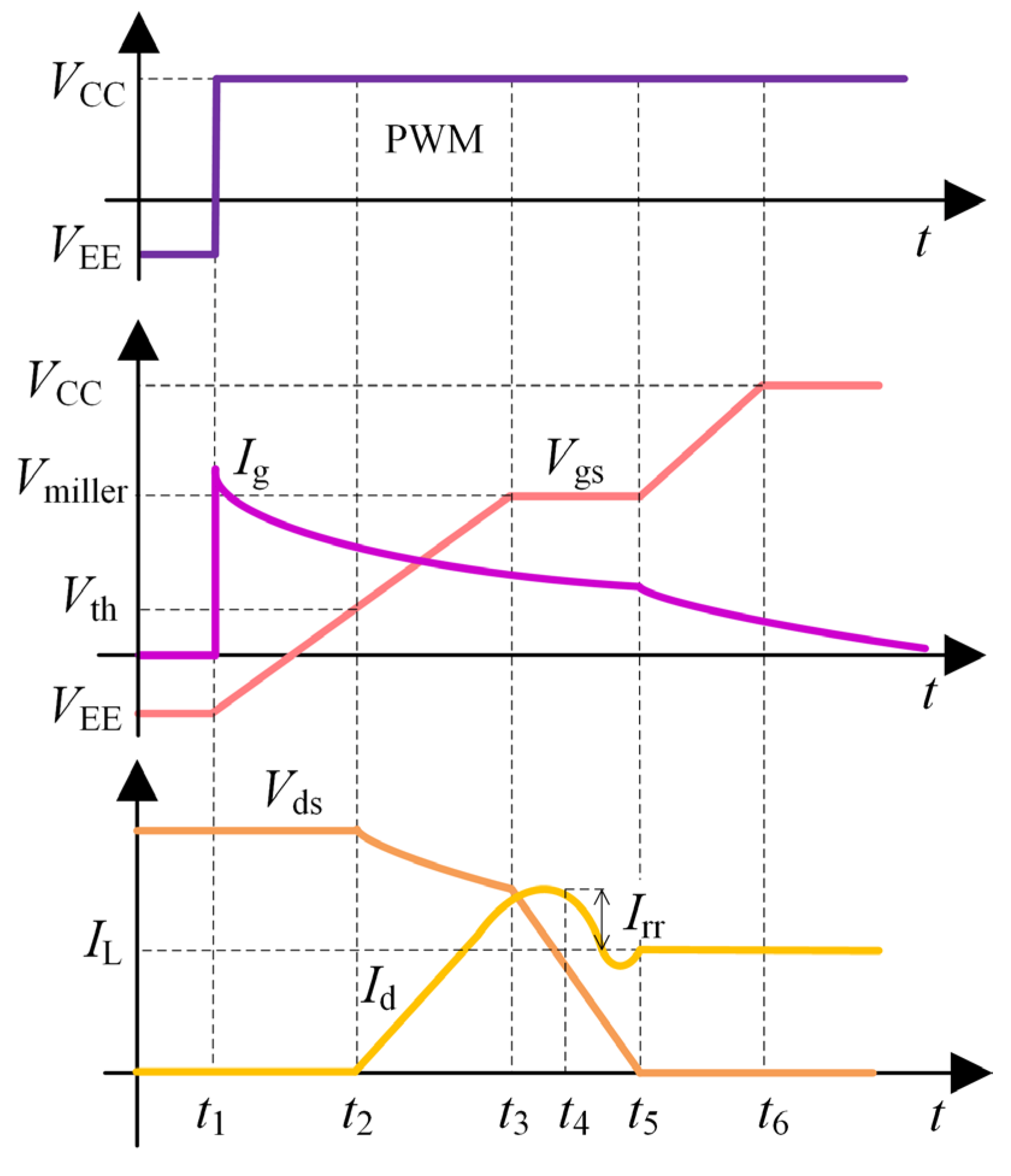
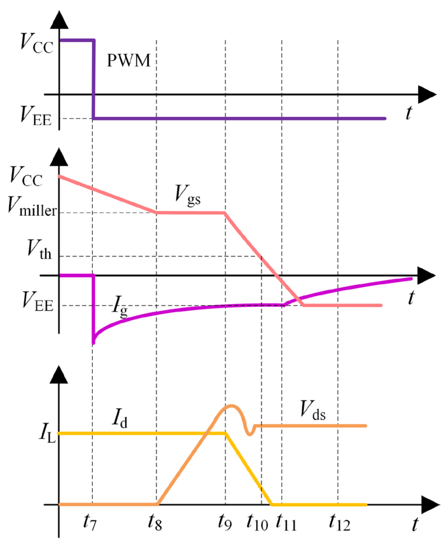
2. Overshoot Analysis of SiC MOSFET Switching Process

Figure 1 illustrates a double pulse test circuit used to analyze the switching process of SiC MOSFETs and measure their switching characteristics [22]. The components in the circuit include Uin (DC input voltage), Cin (energy storage capacitance), Lp (bus parasitic inductance), Lload (load inductance), Q1 (SiC MOSFET under test), Q2 (SiC MOSFET under test), Ld (SiC MOSFET drain parasitic inductance), Ls (SiC MOSFET source parasitic inductance), and Lg (SiC MOSFET gate parasitic inductance). Rg is the gate drive resistor. Df is the SiC MOSFET parasitic diode. Cgs is the SiC MOSFET gate-source parasitic capacitance. Cgd is the SiC MOSFET gate-drain parasitic capacitance and Cds is the SiC MOSFET drain-source parasitic capacitance.
A typical SiC MOSFET turn-on transient waveform is shown in Figure 2. VCC represents the positive driving voltage and VEE represents the negative driving voltage of the SiC MOSFET. Vgs denotes the gate-source voltage, while Ig indicates the driving current. Vmiller refers to the Miller plateau and Vth is the turn-on threshold voltage of the SiC MOSFET. Vds is the voltage across the drain-source terminals and Id is the drain current. Irr represents the drain current overshoot and IL is the load current. The turn-on process of the SiC MOSFET is divided into five stages, which are as follows:
Stage 1 [t1~t2]: Driving voltage rise stage. Vgs increases from VEE to Vth. During this stage, the SiC MOSFET remains in the pinch-off region and does not conduct.
Stage 2 [t2~t3]: Drain current rise stage. At t2, the device transitions from the pinch-off region to the constant current region. Vgs increases from Vth to the Miller platform Vmiller, and Id begins to rise.
Stage 3 [t3~t4]: Drain current overshoot stage. The drain current overshoot is caused by the charging of the junction capacitance of the continuity diode. The charging current Irr is superimposed with the current of the load inductance, resulting in a continuous increase in the SiC MOSFET drain current Id. This current reaches its peak Idpeak at t4. The peak drain current Idpeak can be calculated using Equation (1):
I dpeak = I L + I rr
The peak drain current is influenced by Irr, which is directly proportional to the Id conversion rate, as expressed in Equation (2).
I rr = Q rr d I d d t
The value of Qrr representing the reverse recovery charge of the diode’s junction capacitance can be found in the SiC MOSFET datasheet. The conversion rate of the SiC MOSFET drain current can be calculated using Equation (3).
d I d d t = g fs I g C iss
The input capacitance of the SiC MOSFET, denoted as Ciss, is the sum of Cgs and Cgd. The transconductance gfs of the SiC MOSFET is calculated as follows:
g fs = d I d / d t d V g s / d t
Substituting Equations (3) and (4) into Equation (2) yields Irr as a function of Ig:
I rr = g fs Q rr I g C iss
The current overshoot Irr is directly proportional to the gate current Ig according to Equation (5). To reduce the current overshoot of SiC MOSFETs, it is essential to decrease the gate drive current Ig during the t3~t4 stage. This adjustment will enhance the overall performance and reliability of the SiC MOSFET.
Stage 4 [t4~ t5]: During the drain-source voltage drop stage, Vds rapidly decreases to zero, while Vgs is maintained at Vmiller. The drain current also decreases from its peak to the bus current IL.
Stage 5 [t5~ t6]: The device transitions into the full conduction phase, during which Vgs surpasses Vmiller and rapidly increases to VCC. Vds remains close to zero, with Id equal to IL.
The transient waveform of the SiC MOSFET turn-off is depicted in Figure 3, with all physical quantities in the waveform consistent with the turn-on phase.
Stage 6 [t7~t8]: In the gate drive voltage drop stage, Vgs starts to drop and continues to decrease to Vmiller.
Stage 7 [t8~t9]: The drain-source voltage rise stage begins, with Vds starting to increase while Vgs remains at Vmiller at t8. The input capacitor Ciss continues to discharge through Rg, and Id remains constant.
Stage 8 [t9~t10]: During the drain-source voltage overshoot stage, Id starts to decrease, causing a large induced voltage on the parasitic inductance of the power loop due to the rapidly decreasing Id. This induced voltage, combined with the bus voltage, leads to the formation of the voltage overshoot phenomenon during the shutdown stage. The voltage overshoot spike Vdspeak occurs after this combination. Vgs gradually decreases from Vmiller to Vth.
The voltage overshoot spike can be calculated from Equation (6):
V dspeak = U in L loop d I d d t
The total power loop inductance (Loop) is the sum of the bus circuit inductance, drain inductance, and source inductance of the SiC MOSFET device. When the power loop remains constant, the total power loop inductance (Loop) also remains constant.
The rate of change of the drain current when the device drain-source voltage reaches a spike can be calculated using Equation (7):
d I d d t | V ds = V dspeak = g fs I g C iss
From Equations (4) and (7), it is evident that the rate of change of the drain current can be reduced by lowering Vgs or decreasing Ig, thereby reducing the voltage spike generated during the device’s turn-off process.
Stage 9 [t10~t11]: Drain-source voltage stabilization. At t10, the device transitions from the constant current region to the pinch-off region. Vds stops increasing, exhibits oscillations, and then stabilizes. Id continues to decrease to zero and Vgs continues to fall.
Stage 10 [t11~t12]: Complete device turn-off. Vgs drops to VEE, Vds remains constant, and Id also remains constant.

3. Oscillation Analysis of SiC MOSFET Switching Process

Figure 4 shows the equivalent circuit for the turn-on of the SiC MOSFET, considering the device’s on-resistance Rds(on) [23,24,25]. The parasitic diode Q1 is in reverse cutoff and the drain-source capacitance Cds1 of Q1 is charged.
The gate drive circuit is a series RLC resonant circuit, and its impedance can be expressed by Equation (8) as follows:
Z g = R g + j w on L g + 1 j w on C iss
where won is the resonant angular frequency. The entire turn-on equivalent circuit is also a series RLC resonant circuit, with inductive reactance equal to the capacitive reactance. The resonant angular frequency can be calculated from Equation (9):
w on = 1 L p + L d + L s C ds 1
The circuit shown below features a parallel connection of two impedances at node a, as illustrated in the Equation (10) below:
Z a = Z g × j w on L s Z g + j w on L s
The SiC MOSFET switching oscillations are underdamped and require increased damping to mitigate them. By combining Equations (8) and (10), the impedance at node a can be adjusted by varying the gate drive resistance. Higher gate resistance results in higher impedance and reduced oscillations [26].
The equivalent circuit of the SiC MOSFET during shutdown is depicted on the left side of Figure 5. Here, Q2 is disconnected and Cds2 is charging. The parasitic diode of Q1 is conducting forward, bypassing Cds1 of Q1. On the right side of Figure 5, the parasitic capacitor of Q2, originally in a triangular configuration, is converted to a star configuration.
The impedance of the gate drive circuit at this point is represented by Equation (11):
Z g = R g + j w on L g + 1 j w on C G
won can be calculated by Equation (12):
w on = 1 L p + L d + L s C D + C S
The impedance of the source branch is as follows:
Z s = j w on L s + 1 j w on C S
The circuit impedance below node a is the parallel connection of two impedances; see Equation (14) below:
Z a = Z g × Z s Z g + Z s
By combining Equation (11) with Equation (14), it is evident that reducing oscillation requires increasing the impedance below node a to stabilize the system. Since the parasitic inductance and parasitic capacitance of the SiC MOSFET are constants, the impedance below node a can only be modified by adjusting the gate drive resistance. A higher gate resistance results in higher impedance and, consequently, lower oscillation.

4. Active Gate Driver Circuit Analysis

Based on the above analysis, it is essential to reduce the gate drive current during the t3t4 and t9t10 stages to lower the di/dt, thereby minimizing turn-on transient current overshoot and turn-off transient voltage overshoot [27,28,29]. By examining the oscillation in the switching process of SiC MOSFETs, it is evident that increasing the gate drive resistance can effectively reduce drain current and drain-source voltage oscillation during the switching process.
Figure 6 illustrates the current overshoot suppression circuit. Before Q2 conducts, the gate current is denoted as ig. The gate drive resistor is formed by connecting R1 and Rgon in parallel. The detection circuit utilizes the voltage VLs generated by the source inductor to monitor the conduction state of Q2. The ground of the AGD circuit is defined as SGND. Using this reference point, the source inductor senses the voltage VLs, which can be determined by Equation (15). When VLs reaches a certain value, the instant of Q2 conduction can be identified [30]. Upon detecting Q2 conduction, if the difference between the base voltage Vref of transistor Q3 and the source inductor voltage VLs exceeds 0.7 V, the transistor begins to conduct, initiating the shunt circuit. The gate current ig is then divided into two parts, one of which is igo; thus, the actual gate current is ig1 = igigo, reducing the gate drive current. Meanwhile, the operational amplifier AMP functions as a comparator when Q2 is on. If the source inductor voltage VLs exceeds the reference voltage Vref2, the operational amplifier AMP outputs a low level to turn off Qon. At this point, the gate drive resistance is only Rgon, thereby increasing the gate resistance. Consequently, the reduction in gate current and increase in gate resistance are achieved, mitigating turn-on current overshoots and oscillations. The Vref1 settings can be adjusted according to the working conditions. When VLs is smaller, it can be set to a higher value. To simplify the circuit, this paper sets Vref1 to 0 V. To prevent false triggering of the comparator due to circuit noise, Vref2 cannot be set to 0 V. Therefore, this paper sets Vref2 to 1.2 V.
V L s = L s d i d d t
The transistor Q3 begins to conduct when VrefVLs exceeds 0.7 V. The current igo is diverted from the gate main circuit and can be calculated using Equation (16). At this point, the actual gate drive current ig1 is determined by Equation (17):
i go = V ref 1 V B E V L s R 2
i g 1 = i g i go
The collector-emitter voltage drop of the transistor denoted as VBE, is generally 0.7 V. From Equation (17), it is evident that the shunt current igo increases when VrefVLs is larger, resulting in a decrease in the actual gate drive current ig1. Equation (5) indicates that the turn-on current overshoot can be mitigated by reducing the gate drive current. A lower rate of change in the drain current of the SiC MOSFET leads to a lower current overshoot during turn-on.
As illustrated in Figure 7, the voltage overshoot suppression circuit is shown. Prior to disconnecting Q2, the gate current is represented as ig. The gate drive resistor consists of R2 and Rgoff in parallel. The detection circuit monitors the rate of change of the Q2 drain-source voltage, and the transistor Q4 begins to conduct when the Q2 drain-source voltage changes significantly. At this time, Vref3 injects current igin into the gate drive circuit. If the positive drive current is considered as the positive direction, the gate current is actually |ig|−|igin|, thus reducing the gate drive current. Conversely, when Vf exceeds the reference voltage Vref4, the comparator COM outputs a low level to turn off Qoff. At this time, the gate drive resistance is only Rgoff, thereby increasing the gate resistance. In this way, the gate current decreases and the gate resistance increases, achieving the purpose of reducing the turn-off voltage overshoot and oscillation. Vref3 can be set to a larger value as the injection voltage source; for simplicity, this paper sets Vref3 to +5 V. The Vref4 setting is determined according to the working conditions; considering the high value of Vf, it is set to 5 V in this paper.
The detection circuit samples the drain voltage using an RC differential circuit. Vf represents the sampled voltage, Rf is the sampling resistor, and Cf is the sampling capacitance [31]. As shown in Equation (18), Vf characterizes the rate of change of the drain voltage:
V f = R 5 C f d V ds d t
The current direction at the turn-on moment is defined as positive. To reduce the gate drive current at the turn-off moment, it is necessary to inject current. At this point, the gate drive current can be calculated using Equation (19):
i g 2 = i g + i gin
The injected current magnitude can be determined from the circuit diagram using Equation (20). By decreasing the values of R4 and R3, the injection current can be increased, which in turn increases the reverse gate drive current and reduces the drain-source voltage overshoot.
i gin = V ref 3 R 4 + V f R 3

5. Experimental Analysis

Based on the working principle and design results detailed in Section 4, we conducted PSpice double pulse simulation experiments. We utilized a silicon carbide device provided by Wolfspeed (model C3M0015065K). The hardware platform depicted in Figure 8 was assembled to validate the proposed circuits experimentally. Experiments were performed using an STM32F103C8T6 core control board to generate double pulses. The current probe model used was ETA5520A, and the high-voltage active differential probe was ETA5010. The oscilloscope model employed was DS2102E.

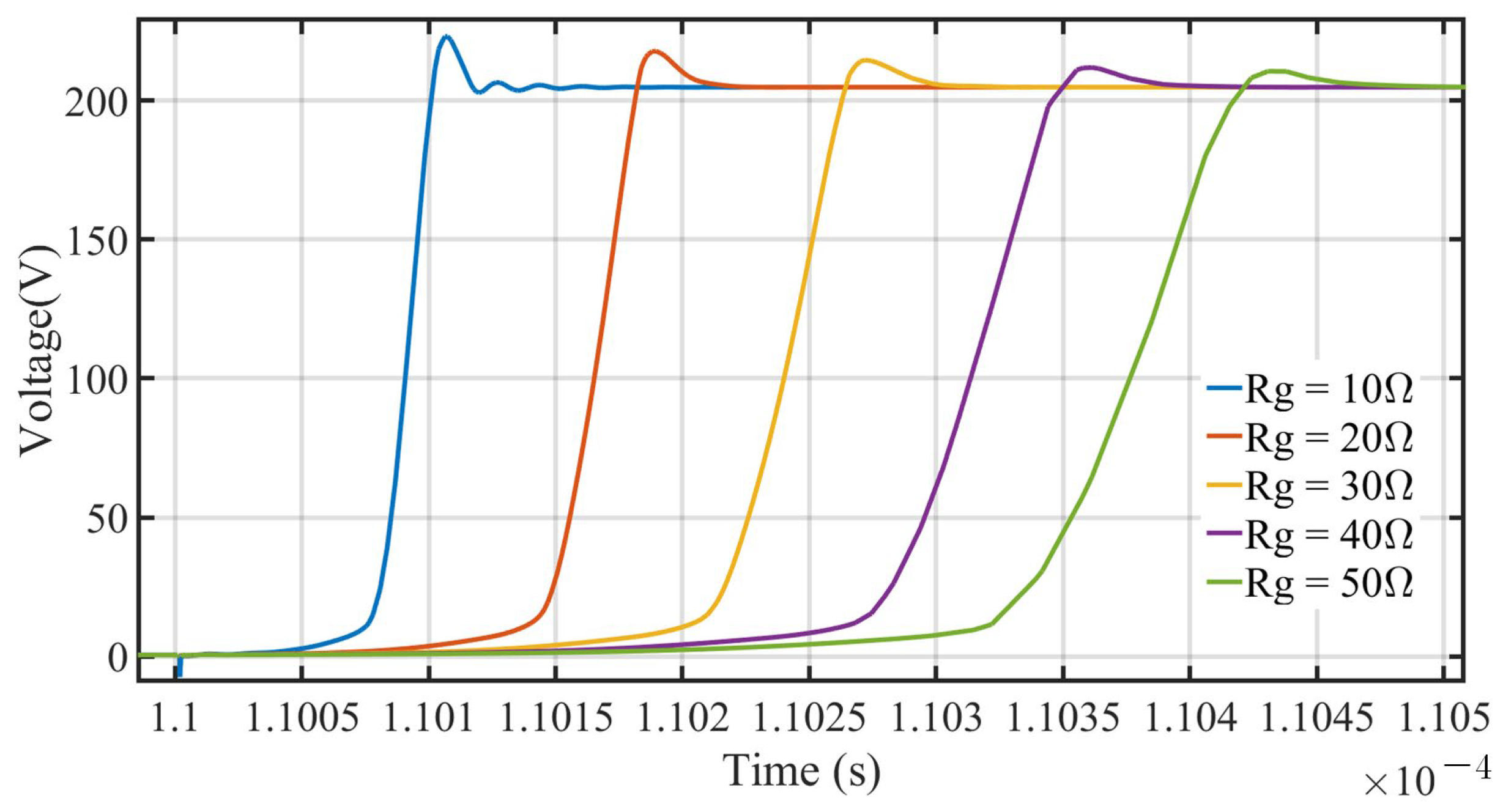
5.1. Experiments With Different Gate Resistors

The simulated test waveforms shown in Figure 9 illustrate the impact of different gate resistances on the turn-on current. When comparing the turn-on current waveforms of SiC MOSFETs with gate driving resistances of 10 Ω, 20 Ω, 30 Ω, 40 Ω, and 50 Ω, it is evident that larger gate resistances extend the time required for the MOSFET to transition from the cutoff state to the saturated conduction state. This results in a slower rise of Id, reduced Id overshoot, and minimized oscillations. The turn-on time increases with higher gate drive resistance because a larger resistance limits the gate drive current, leading to an increase in the gate capacitor’s charging and discharging times. This delay impacts both the turn-on and turn-off processes of the SiC MOSFET.
Figure 10 illustrates the simulated waveforms depicting the impact of various gate resistors on the turn-off voltage of SiC MOSFETs. We compared the turn-off voltage waveforms for gate drive resistances of 10 Ω, 20 Ω, 30 Ω, 40 Ω, and 50 Ω. An increase in drive resistance extends the discharge time required for the gate voltage to transition from the on state to the off state, resulting in a longer turn-off delay time for the MOSFET. Higher gate drive resistance decelerates the discharge of the gate charge, prolonging the entire turn-off process and increasing turn-off losses. A larger gate resistor helps to reduce di/dt, effectively minimizing Vds overshoots and oscillations. However, the reverse recovery time of the body diode may increase due to the slower turn-off speed, raising the risk of Vds overshoot caused by parasitic inductance.

5.2. Comparison of the Effects of AGD and CGD Circuits under Various Operational Conditions

Figure 11 presents the comparison of AGD and CGD effects under four different load currents (20 A, 40 A, 60 A, 80 A). The current overshoot is reduced by 44.73% at 20 A, as shown in Figure 11a; 52.38% at 40 A, as shown in Figure 11b; 56.52% at 60 A, as shown in Figure 11c; and 58.33% at 80 A, as shown in Figure 11d. It is evident that the higher the load current, the higher the parasitic inductor voltage at the source of the SiC MOSFET. Consequently, the current overshoot suppression circuit draws more current from the gate, significantly reducing the turn-on current overshoot.
As shown in Figure 12, a comparison of the effects of AGD and CGD at four different bus voltages is recorded for 100 V, 200 V, 300 V, and 400 V. The voltage overshoot is reduced by 37.50% at a bus voltage of 100 V, as shown in Figure 12a. At 200 V, the voltage overshoot is reduced by 38.46%, as shown in Figure 12b. At 300 V, the voltage overshoot is reduced by 39.13%, as shown in Figure 12c. At 400 V, the voltage overshoot is reduced by 40.74%, as shown in Figure 12d. The higher the bus voltage, the greater the drain-source voltage change rate of the SiC MOSFET. Consequently, more current is injected into the gate by the voltage overshoot suppression circuit, leading to a greater reduction in the turn-off voltage overshoot.

5.3. Comparison of AGD Circuit and CGD Circuit Effects

The hardware experimental conditions for the AGD and CGD drain current experiments were set with a bus voltage of 50 V and a load inductance of 500 µH. The driver resistor used for the experiment was 15 Ω. As shown in Figure 13, the experimental comparison of AGD and CGD drain currents indicates that the drain current overshoot is 2.5 A for CGD and 1 A for AGD. AGD reduces the drain current overshoot by 60% compared to CGD, and significantly diminishes the magnitude and duration of drain current waveform oscillations.
Figure 14 presents an experimental comparison of AGD and CGD drain-source voltages. The drain-source voltage overshoot is 180 V with CGD and 160 V with AGD. AGD lowers the drain-source voltage overshoot by 15.38% compared to CGD and considerably reduces the magnitude and duration of the drain-source voltage waveform oscillations. These results demonstrate that the proposed AGD circuit effectively suppresses the turn-on current, turn-off voltage overshoot, and oscillations of SiC MOSFETs.
Table 1 compares the overshoot and loss characteristics of SiC MOSFETs for both AGD and CGD circuits. It is evident from the table that the AGD circuit significantly reduces turn-on current overshoot and turn-off voltage overshoot. Additionally, the turn-on and turn-off losses of the AGD circuit are reduced by an average of 24%.
In practical applications of SiC MOSFETs, high di/dt and high dv/dt are key factors causing EMI problems. To analyze the EMI of SiC MOSFETs using the AGD circuit, the drain current (Id) and drain-source voltage (Vdc) of the AGD and CGD circuits were analyzed using fast Fourier transforms (FFTs), as shown in Figure 15. The AGD circuit proposed in this paper was observed to not have a negative impact on EMI compared to CGD. In the spectrogram of the drain current circuit in Figure 15a, the AGD driver circuit does not cause EMI problems in the 0.1–6 MHz band relative to the CGD driver circuit. It even improves the EMI issue in the 0.5–2 MHz band. In the drain-source voltage spectrum in Figure 15b, the AGD driver circuit improves the EMI problem in the 0.1–10 MHz band compared to the CGD driver circuit.
In summary, the AGD circuit proposed in this paper enhances switching speed while significantly reducing current and voltage overshoot, as well as losses. Additionally, this AGD circuit does not negatively impact EMI and even improves EMI issues in certain frequency bands.

5.4. Comparison of AGD Circuit and RCD Snubber Circuit Effects

The schematic diagram of the RCD snubber circuit is shown in Figure 16. When the SiC MOSFET is on, the current in the circuit mainly flows through the main circuit, and the RCD snubber does not work at this time. At the instant the SiC MOSFET turns off, the current in the circuit charges the capacitor CSNB through the diode DSNB of the RCD snubber circuit. Since the voltage across CSNB cannot change abruptly, the rate of rise of the switching voltage of the switching tube is reduced. This reduces the turn-off voltage overshoot and transfers the turn-off power loss from the switching tube to the RSNB.
Figure 17 presents a comparison of the waveforms of the three circuits at a bus voltage of 200 V. The overshoot of the CGD circuit is 14.5%, the RCD snubber circuit is 10.75%, and the AGD circuit is 7%. Regarding oscillations, both the AGD circuit and the RCD snubber circuit effectively reduce voltage oscillations. However, the AGD circuit is more effective with an oscillation time of only 14 ns.
Figure 18 shows a comparison of the waveforms of the three circuits at a load current of 40 A. The peak current of the CGD circuit is 61 A, the RCD snubber circuit is 60 A, and the AGD circuit is 48 A. It is evident that the RCD snubber circuit does not significantly reduce the turn-on current spike of the SiC MOSFET. In terms of oscillation, the AGD circuit demonstrates the most significant reduction.
Therefore, the AGD circuit outperforms the RCD snubber circuit in reducing the turn-on current, the turn-off voltage overshoot, and oscillations of the SiC MOSFET.

6. Conclusions

This paper began with a detailed stage-by-stage analysis of the switching transient process of SiC MOSFETs. The fundamental causes of turn-on transient current overshoot and turn-off voltage overshoot were examined, along with a thorough analysis of the oscillation phenomena that accompany the switching action. Based on these findings, a triode with a dynamic switching strategy was designed as an active driver circuit. This circuit separates and injects control current into the gate during the current and voltage spike phases of the SiC MOSFET, complemented by a targeted drive resistor configuration. This effectively reduces peak turn-on transient current and suppresses turn-off voltage overshoot, simultaneously minimizing switching oscillations.
Compared to the CGD circuit and RCD snubber circuit, this design performs better in suppressing overshoot and oscillation. Among most active drive technologies, the primary advantage of this solution lies in its clean and simple structural design and ease of implementation. It demonstrates good adaptability and excellent suppression performance under various operating conditions, showcasing a high degree of versatility. Future research will focus on further improving overall performance, particularly in areas such as precise detection of hardware parameters and optimization of key parameter combinations.

Author Contributions

Author contributions: Conceptualization, Y.L. and Y.Y.; methodology, Y.L. and Y.Y.; software, J.Y.; validation, Y.L. and H.W.; formal analysis, C.H.; investigation, Y.Y.; resources, Y.Y. and C.H.; data curation, Y.Y.; writing—original draft preparation, Y.L.; writing—review and editing, Y.L. and Y.Y.; visualization, J.Y.; supervision, H.W.; project administration, Y.L.; funding acquisition, Y.L. and Y.Y. All authors have read and agreed to the published version of the manuscript.

Funding

This research was funded by the Natural Science Foundation of Guangxi Province of China, grant number 2021GXNSFAA220038.

Data Availability Statement

Data is contained within the article.

Acknowledgments

The authors would like to acknowledge the financial support provided by the Opening Project of Key Laboratory of Advanced Manufacturing and Automation Technology, Guilin University of Technology.

Conflicts of Interest

Author Changbin Huang was employed by the company Greatwall Power Supply Technology Co., Ltd. The remaining authors declare that the research was conducted in the absence of any commercial or financial relationships that could be construed as potential conflicts of interest.

References

  1. Sheng, K.; Renm, N.; Xu, H. A Recent Review on Silicon Carbide Power Devices Technologies. Proc. CSEE 2020, 40, 1741–1752. [Google Scholar]
  2. Zhang, L.; Yuan, X.; Wu, X.; Shi, C.; Zhang, J.; Zhang, Y. Performance evaluation of high-power SiC MOSFET modules in comparison to Si IGBT modules. IEEE Trans. Power Electron. 2019, 34, 1181–1196. [Google Scholar] [CrossRef]
  3. Yang, L.; Li, K.; Dai, J.; Corfield, M.; Harris, A.; Paciura, K.; O’Brien, J.; Johnson, C.M. Electrical performance and reliability characterization of a SiC MOSFET power module with embedded decoupling capacitors. IEEE Trans. Power Electron. 2018, 33, 10594–10601. [Google Scholar] [CrossRef]
  4. Zhao, S.; Zhao, X.; Dearien, A.; Wu, Y.; Zhao, Y.; Mantooth, H.A. An intelligent versatile model-based trajectory-optimized active gate driver for silicon carbide devices. IEEE J. Emerg. Sel. Top. Power Electron. 2020, 8, 429–441. [Google Scholar] [CrossRef]
  5. Jacobs, K.; Heinig, S.; Johannesson, D.; Norrga, S.; Nee, H.P. Comparative evaluation of voltage source converters with silicon carbide semiconductor devices for high-voltage direct current transmission. IEEE Trans. Power Electron. 2021, 36, 8887–8906. [Google Scholar] [CrossRef]
  6. Sukhatme, Y.; Miryala, V.K.; Ganesan, P.; Hatua, K. Digitally controlled gate current source-based active gate driver for silicon carbide MOSFETs. IEEE Trans. Ind. Electron. 2020, 67, 10121–10133. [Google Scholar] [CrossRef]
  7. Lina, W.; Zeduo, Y.; Junming, C.; Wu, Z. Overview of Switching Transient Analytical Modeling of SiC MOSFET. Proc. CSEE 2023, 1–13. [Google Scholar]
  8. Xu, C.; Miao, Y. SiC MOSFET Active Gate Drive Circuit Based on Switching Transient Feedback. Energies 2024, 17, 1997. [Google Scholar] [CrossRef]
  9. Guo, R.; Yu, T.; Sun, G.; Liu, W. Optimization analysis and design of DC solid-state circuit breaker buffer circuit based on RCD and MOV. High Volt. Technol. 2019, 45, 2418–2424. [Google Scholar]
  10. Chen, J.; Zhang, W.J.; Shorten, A.; Yu, J.; Sasaki, M.; Kawashima, T.; Nishio, H.; Ng, W.T. A smart IGBT gate driver IC with temperature compensated collector current sensing. IEEE Trans. Power Electron. 2019, 34, 4613–4627. [Google Scholar] [CrossRef]
  11. Lobsiger, Y.; Kolar, J.W. Closed-loop IGBT gate drive featuring highly dynamic di/dt and dv/dt control. In Proceedings of the IEEE Energy Conversion Congress and Exposition (ECCE), Raleigh, NC, USA, 15–20 September 2012; pp. 4754–4761. [Google Scholar]
  12. Camacho, A.P.; Sala, V.; Ghorbani, H.; Martinez, J.L.R. A novel active gate driver for improving SiC MOSFET switching trajectory. IEEE Trans. Ind. Electron. 2017, 64, 9032–9042. [Google Scholar] [CrossRef]
  13. Paredes, A.; Fernandez, E.; Sala, V.; Ghorbani, H.; Romeral, L. Switching trajectory improvement of Sic MOSFET devices using a feedback gate driver. In Proceedings of the 2018 IEEE International Conference on Industrial Technology (ICIT), Lyon, France, 20–22 February 2018; pp. 847–852. [Google Scholar]
  14. Zhao, S.; Zhao, X.; Wei, Y.; Zhao, Y.; Mantooth, H.A. A review of switching slew rate control for silicon carbide devices using active gate drivers. IEEE J. Emerg. Sel. Topics Power Electron. 2021, 9, 4096–4114. [Google Scholar] [CrossRef]
  15. Cao, J.; Zhou, Z.-K.; Shi, Y.; Zhang, B. An integrated gate driver based on SiC MOSFETs adaptive multi-level control technique. IEEE Trans. Circuits Syst. I Reg. 2023, 70, 1805–1816. [Google Scholar] [CrossRef]
  16. Rødal, G.L.; Peftitsis, D. An adaptive current-source gate driver for high-voltage SiC MOSFETs. IEEE Trans. Power Electron. 2023, 38, 1732–1746. [Google Scholar] [CrossRef]
  17. Rødal, G.L.; Peftitsis, D. Gate-Drive Circuits for Adaptive Operation of SiC mosfets. IEEE Trans. Power Electron. 2024, 39, 8162–8186. [Google Scholar] [CrossRef]
  18. Ling, Y.; Zhao, Z.; Zhu, Y. A self-regulating gate driver for high-power IGBTs. IEEE Trans. Power Electron. 2021, 36, 3450–3461. [Google Scholar] [CrossRef]
  19. Chen, Y.; Guo, X.; Bu, X.; Hao, R.; You, X. Optimization method for turn-off trajectory of SiC MOSFET active driving circuit. J. Beijing Jiaotong Univ. 2023, 47, 126–135. [Google Scholar]
  20. Miryala, V.K.; Hatua, K. Low-cost analogue active gate driver for SiC MOSFET to enable operation in higher parasitic environment. IET Power Electron. 2020, 13, 463–474. [Google Scholar] [CrossRef]
  21. Li, X. An Active Gate Driver Circuit for Suppressing Voltage and Current Overshoots of SiC MOSFETs. J. Semicond. Technol. 2023, 48, 1006–1011+1029. [Google Scholar]
  22. Yang, C.; Pei, Y.; Wang, L.; Yu, L.; Zhang, F.; Ferreira, B. Overvoltage and oscillation suppression circuit with switching losses optimization and clamping energy feedback for SiC MOSFET. IEEE Trans. Power Electron. 2021, 36, 14207–14219. [Google Scholar] [CrossRef]
  23. Wu, Y.; Yin, S.; Li, H.; Ma, W. Impact of RC snubber on switch in go scillation damping of SiC MOSFET with analytical model. IEEE J. Emerg. 2020, 8, 163–178. [Google Scholar]
  24. Lee, S.; Chen, F.; Jahns, T.M.; Sarlioglu, B. Topological Equivalence of VSI and CSI Commutation Cells and Its Application to Switching Resonance Analysis and Damper Design. IEEE Trans. Transp. Electrif. 2024, 10, 1363–1376. [Google Scholar] [CrossRef]
  25. Wang, X.; Yang, X.; Liu, G. Investigation for Influence of Parasitic Inductances of Damping Resistors on Suppressing SiC MOSFET Switching Oscillation. In Proceedings of the 2023 IEEE 2nd International Power Electronics and Application Symposium (PEAS), Guangzhou, China, 10–13 November 2023; pp. 1819–1825. [Google Scholar]
  26. Li, J.; Yang, X.; Xu, M.; Wang, X.; Heng, K. A novel inductively coupled RLC damping circuits for eliminating switching oscillations of SiC MOSFET. IET Power Electron. 2023, 16, 1486–1498. [Google Scholar] [CrossRef]
  27. Wang, N.; Zhang, J. Review of Active Gate Driver for SiC MOSFET with Switching Trajectory Optimization. J. Electrotechnol. 2022, 37, 2523–2537. [Google Scholar]
  28. Peng, H.; Peng, H.; Yue, Q. Resonant gate driver with wide range adjustment of driving speed. In Proceedings of the 2021 IEEE Workshop on Wide Bandgap Power Devices and Applications in Asia (WiPDA Asia), Wuhan, China, 25–27 August 2021; pp. 371–375. [Google Scholar]
  29. Yue, Q.; Peng, H.; Tong, Q.; Kang, Y. A Novel Driving Current Control Approach in Enhanced Current-Source Gate Driver. IEEE Trans. Power Electron. 2023, 38, 10563–10568. [Google Scholar] [CrossRef]
  30. He, Y.; Wang, X.; Shao, S.; Zhang, J. Active gate driver for dynamic current balancing of parallel-connected SiC MOSFET. IEEE Trans. Power Electron. 2023, 38, 6116–6127. [Google Scholar] [CrossRef]
  31. Qiu, J. Modeling of SIC MOSFET And Research of Active Gate Drive Circuit. Master’s Thesis, Harbin Institute of Technology, Harbin, China, 2022. [Google Scholar]
Figure 1. Double pulse test circuit.
Electronics 13 03020 g001
Figure 2. SiC MOSFET turn-on process waveforms.
Electronics 13 03020 g002
Figure 3. SiC MOSFET shutdown process waveforms.
Electronics 13 03020 g003
Figure 4. Turn-on equivalent circuit.
Electronics 13 03020 g004
Figure 5. Shutdown equivalent circuit.
Electronics 13 03020 g005
Figure 6. Current overshoot suppression circuit.
Electronics 13 03020 g006
Figure 7. Voltage overshoot suppression circuit.
Electronics 13 03020 g007
Figure 8. Double pulse experimental platform.
Electronics 13 03020 g008
Figure 9. Comparison of turn-on current waveforms of SiC MOSFETs with different gate driving resistances.
Electronics 13 03020 g009
Figure 10. Comparison of turn off voltage waveforms of SiC MOSFETs with different gate driving resistances.
Electronics 13 03020 g010
Figure 11. Comparison of AGD and CGD turn-on current waveforms for different load currents: (a) 20 A load current; (b) 40 A load current; (c) 60 A load current; (d) 80 A load current.
Electronics 13 03020 g011
Figure 12. Comparison of AGD and CGD turn-off voltage waveforms for different bus voltages: (a) 100 V bus voltage; (b) 200 V bus voltage; (c) 300 V bus voltage; (d) 400 V bus voltage.
Electronics 13 03020 g012
Figure 13. Comparison of AGD and CGD drain current experiments.
Electronics 13 03020 g013
Figure 14. Experimental comparison of AGD and CGD drain-source voltages.
Electronics 13 03020 g014
Figure 15. Comparison of spectrograms between AGD and CGD circuits: (a) Id spectrogram; (b) Vdc spectrogram.
Electronics 13 03020 g015
Figure 16. Schematic diagram of RCD snubber.
Electronics 13 03020 g016
Figure 17. Comparison experiment waveforms for 200 V bus voltage.
Electronics 13 03020 g017
Figure 18. Voltage comparison experiment waveform for 40 A load.
Electronics 13 03020 g018
Table 1. Comparison of overshoot and loss of SiC MOSFETs with AGD and CGD.
StageProgrammaticOvershootSwitching Loss
Opening
stage
CGD15 A1.859 mJ
AGD13.5 A1.448 mJ
Closing
stage
CGD180 V1.969 mJ
AGD160 V1.366 mJ
Disclaimer/Publisher’s Note: The statements, opinions and data contained in all publications are solely those of the individual author(s) and contributor(s) and not of MDPI and/or the editor(s). MDPI and/or the editor(s) disclaim responsibility for any injury to people or property resulting from any ideas, methods, instructions or products referred to in the content.

