Abstract
A novel compact broadband negative group delay (NGD) circuit with flatness and bandwidth enhancement is presented. The presented negative group delay circuit (NGDC) consists of a high-impedance transmission line connected by two resistors, which are linked together with two coupled lines and a low-impedance transmission line. The flatness of the NGD is enhanced by tuning the characteristic impedance of the transmission lines. In order to verify the method, a compact broadband NGDC with a size of 29.4 mm × 58.1 mm (0.14 λg × 0.29 λg) is designed, fabricated, and measured at the center frequency of 1.0 GHz. The measured results show that an NGD time of −0.49 ns at the center frequency is obtained with return loss and insertion loss of 35.0 dB and 18 dB, respectively. And, the flat-NGD bandwidth reaches 509 MHz (50.9%) over 0.766 to 1.275 GHz with 19% group-delay fluctuation.
1. Introduction
Recently, negative group delay circuits (NGDCs) have attracted more attention due to their potential applications. The NGDCs have been employed for amplifiers to achieve group delay (GD) equalization [1], to achieve the compensation of the beam squint in series-fed antenna arrays [2] and to improve the performance of signal anticipation [3], and kinds of filters were designed with the NGD characteristic [4,5,6]. In [7], the NGDCs were used in designing non-foster components. Furthermore, reconfigurable non-foster circuits with NGDCs were designed [8]. Besides, the compensation of GD [9] or the anticipation of the mechanical actuators’ signals [10] can be achieved by cascading the NGDCs and other components. In order to obtain high performance, some NGDCs based on new methods such as filter theory [11], signal interference techniques [12], lossy transmission lines [13] and split-ring resonators [14] have been presented. However, the GD near the center frequency is not flat and cannot satisfy wideband applications such as the broadband phase shifter [15].
In order to increase the flatness of the GD, several flat-NGDCs have been presented [16,17,18,19,20,21,22,23,24]. In accordance with filter theory, a 4.3% flat-NGD bandwidth of a NGDC with a ripple of 16% was achieved [16]. In [17], through bringing the two working frequencies of the dual-band NGDC closer, a flat-NGDC was designed. But the absolute flattening of GD cannot be achieved in theory. Afterwards, power dividers with flat-NGD characteristics were proposed in [18,19,20]. In addition, based on the transmission lines with step impedance or T-type structures, a flat NGD characteristic with an NGD time of −0.5 ns and −1.11 ns was achieved [21,22]. Nevertheless, the circuit size was not small enough. To achieve the size reduction, two NGDCs based on two TL structures and three coupled lines were presented, respectively [23,24]. However, the ideal port matching characteristics could not be obtained, and the circuit size needed to be further enhanced.
In this paper, a compact broadband NGDC is presented to achieve flat-NGD characteristics and ideal port matching. The presented NGDC consists of two couple lines connected by a transmission line and two resistors linked with a transmission line. The couple lines are utilized to improve the port matching characteristics and the two transmission lines are used to strengthen the flatness of the NGD response. And, the equivalent of the open-circuited coupled line is a Π structure [25]. Therefore, compared with the circuit in [23], the proposed circuit structure with the coupled lines is completely different. Furthermore, under the condition of the flat-NGD characteristic, the ideal port matching of the proposed circuit is realized. The circuit and design process are presented and discussed.
2. Circuit Structure and Design Theory
2.1. Even- and Odd-Mode Analysis
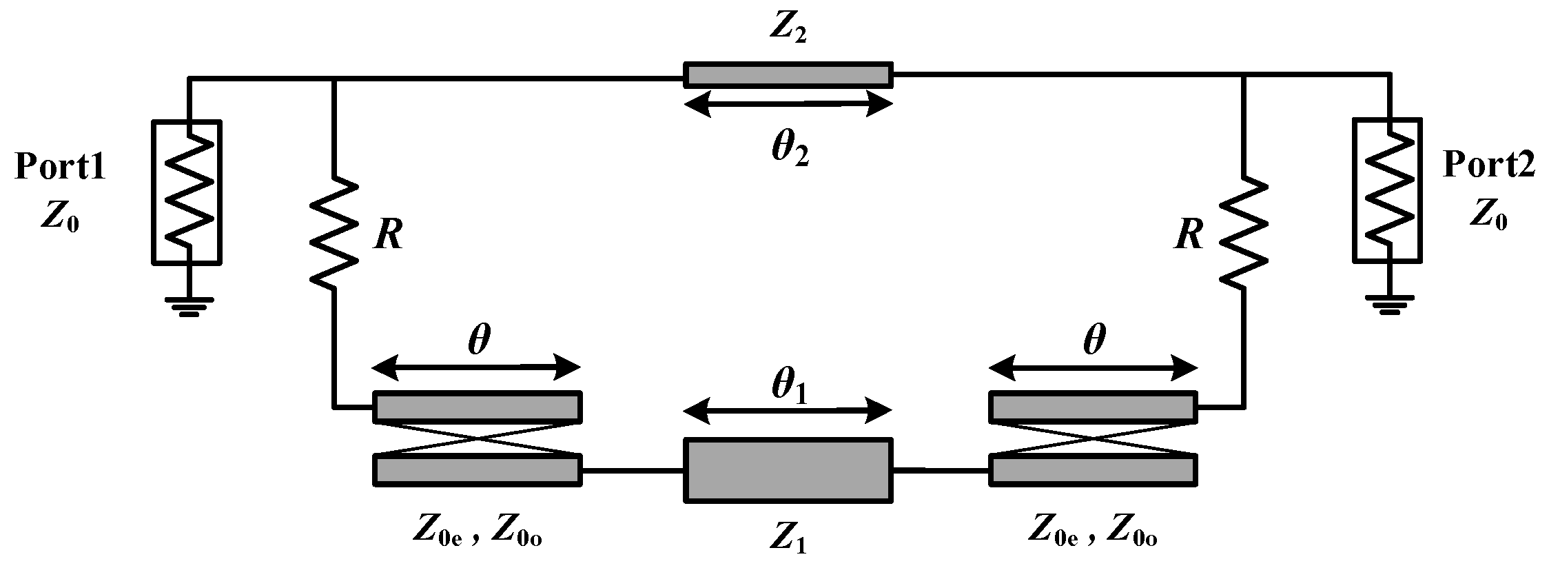
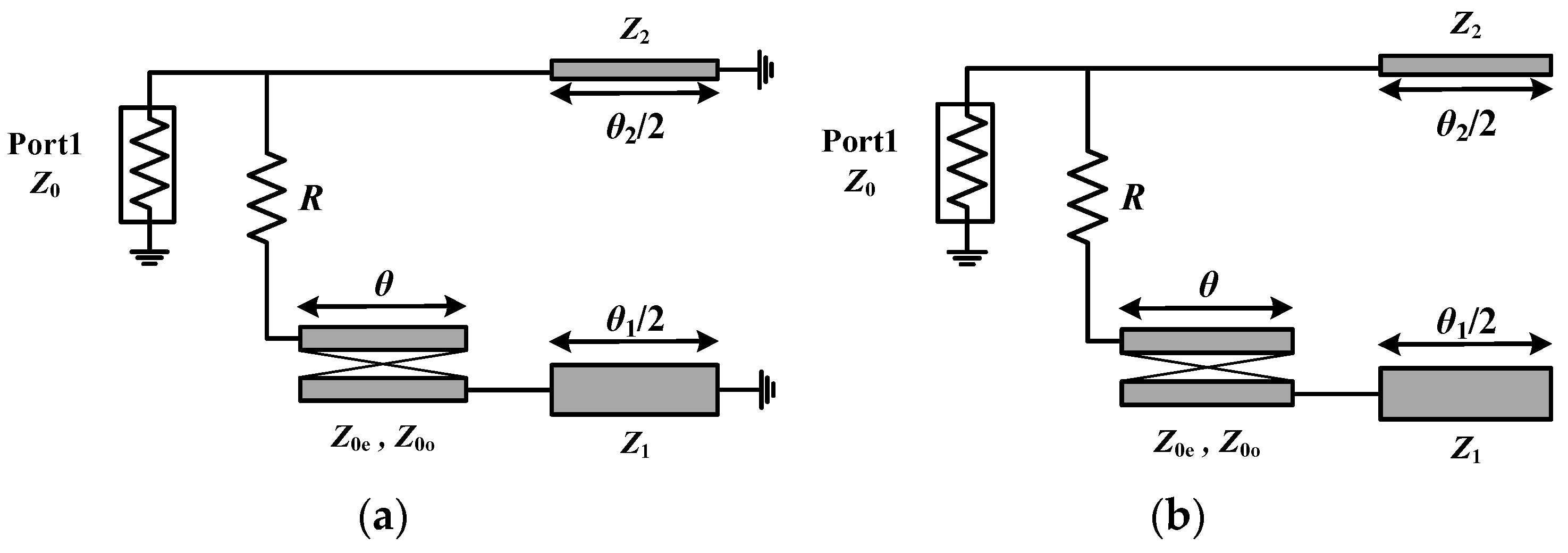
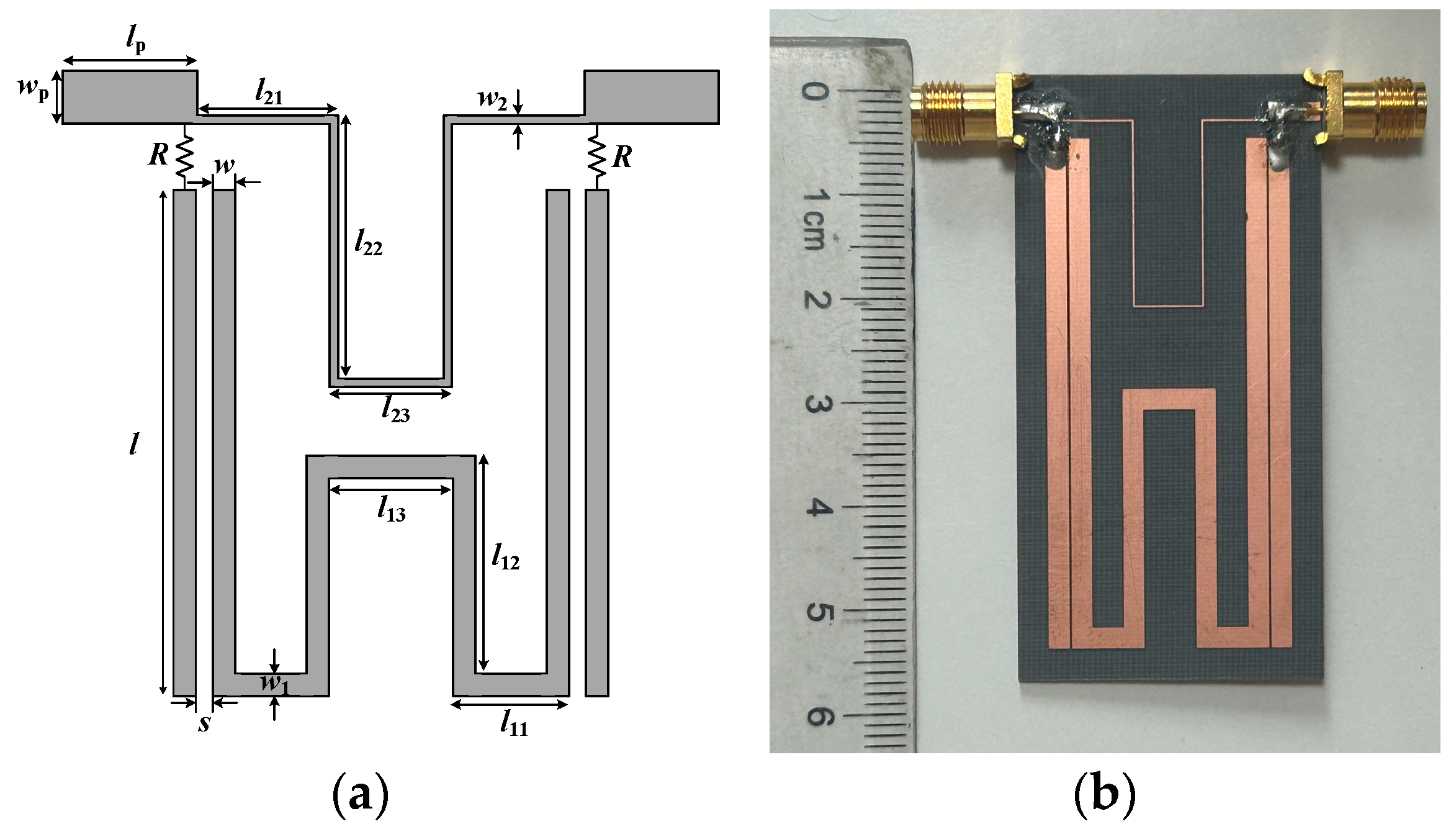
Figure 1 gives the configuration of the proposed compact broadband NGDC. It consists of two couple lines with even- and odd-mode characteristic impedance Z0e, Z0o and electrical length θ, which is connected by a transmission line with characteristic impedance Z1 and electrical length θ1, and two resistors R link, by transmission line, with characteristic impedance Z2 and electrical length θ2.
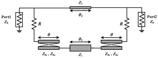
Figure 1.
Configuration of the proposed NGD microwave circuit.
The even- and odd-mode equivalent circuits of the proposed NGDC is shown in Figure 2. And, the even- and odd-mode input impedance Zin_odd and Zin_even can be expressed as
where A1, A2, A3 and A4 are given in Equations (3)–(6).
where the expression of Modd and Meven are

Figure 2.
Odd- and even-mode equivalent circuits. (a) Odd-mode; (b) even-mode.
And then the S-parameters of the presented compact broadband NGDC are expressed as
where Z0 is the port impedance. The unknown parameters in Equation (10) are
Furthermore, the GD of the presented NGDC can be expressed as
2.2. S-Parameters and NGD Analysis
In the proposed compact broadband NGDC, the electronic length is assumed as θ1 = θ2 = θ = π/2 at center frequency f0. When the electronic lengths in Equations (1)–(15) are π/2, the simplification of S-parameters and GD at f0 are
where the unknown parameters are given as
where P and Q can be expressed as
As can be seen from the expressions of S11(f0), S21(f0) and GD(f0) in Equations (16)–(18), there are four variables Z2, R, P and Q in them. So, if Z2 is determined, the values of R, P and Q can be solved for. Once P and Q are known, there are only three variables, Z1, Z0e and Z0o, in Equations (24) and (25). When Z1 is determined, the values of Z0e and Z0o can also be solved for.
Therefore, it is a must to determine the desired values of the S11(f0), S21(f0) and GD(f0) ahead and chose proper values of the free variables Z1 and Z2 during the design.
2.3. Free Variables Analysis
Based on the theory in Section 2.2, when S11(f0) = 0 for port matching, the values of S21(f0) and GD(f0) can be selected according to different needs of designers. In this section, the GD and S-parameters, especially the flat-NGD bandwidth and flatness, of the free variables Z1 and Z2 at different values will be discussed.
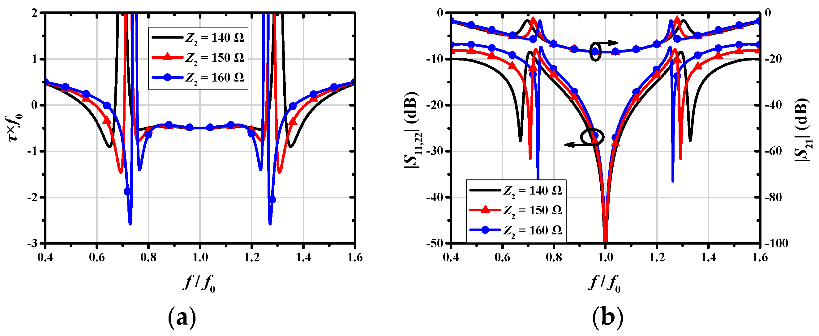
Figure 3 gives the influences of Z2 on the GD and S-parameters. It can be seen that when Z2 increases from 140 Ω to 160 Ω, the ripple of τg × f0 near the center frequency f0 increases. Moreover, |S11| and |S21| change a little within the flat-NGD bandwidth. Consequently, Z2 can be employed to additionally improve the flatness of GD.

Figure 3.
The performance at different Z2 values with fixed Z1 = 60 Ω, τg × f0 = −0.5 and |S21| = −17 dB at f0. (a) τg × f0; (b) S−parameters.
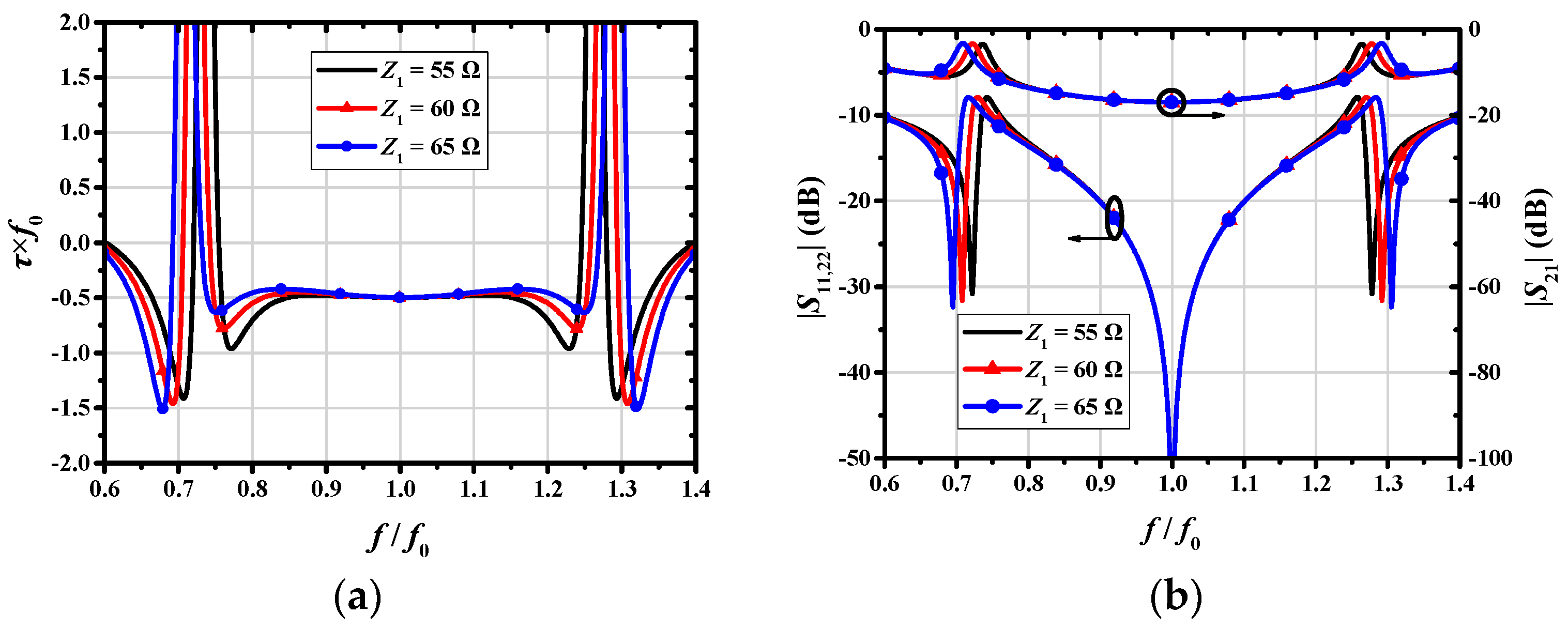
The changes in circuit performances with different values for Z1 are given in Figure 4. As can be seen, when Z2 increases from 55 Ω to 65 Ω, the ripple of τg × f0 near the center frequency f0 decreases. Moreover, |S11| and |S21| remain unchanged within the flat-NGD bandwidth. Consequently, Z1 can also be used to achieve the GD flatness enhancement.
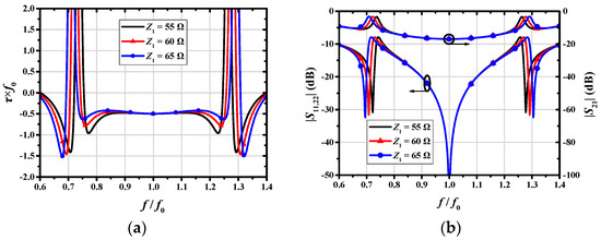
Figure 4.
The performance at different Z1 values with fixed Z2 = 150 Ω, τg × f0 = −0.5 and |S21| = −17 dB at f0. (a) τg × f0; (b) S−parameters.
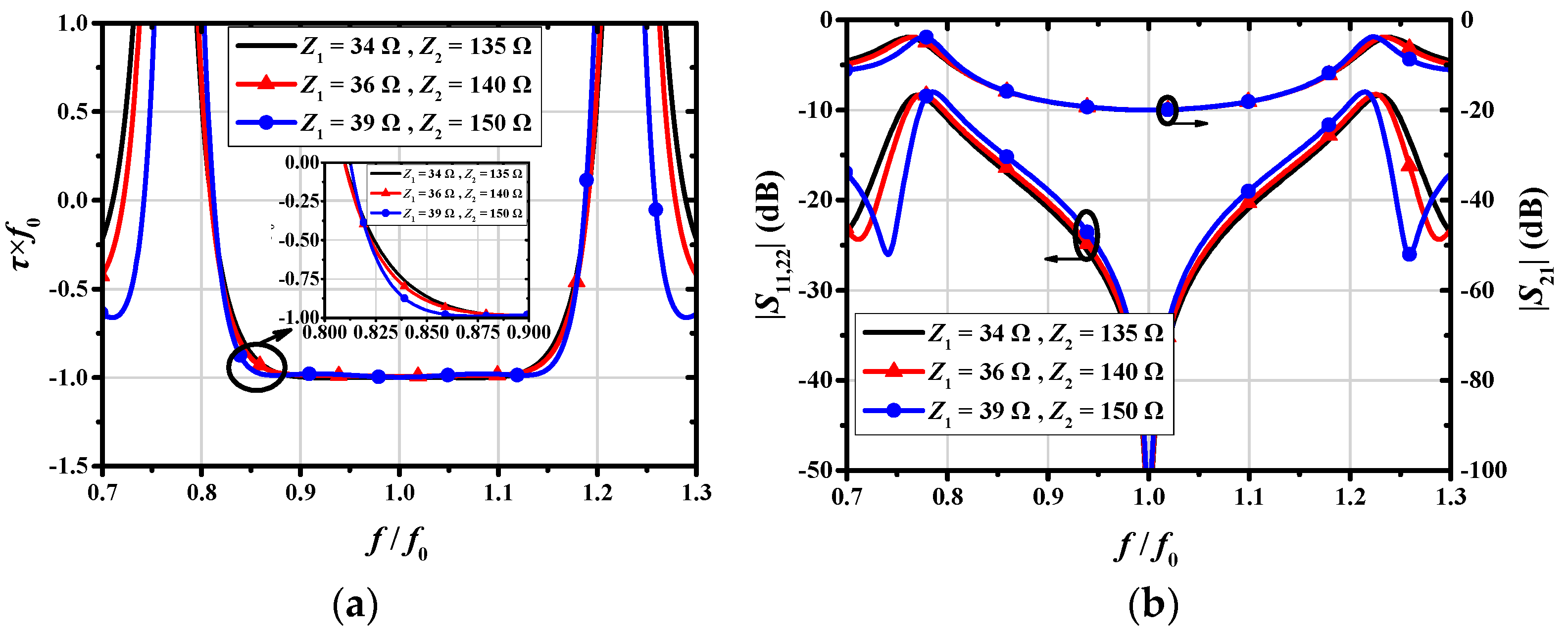
Figure 5 shows the effect of different Z1 and Z2 couples on the entire circuit’s performance. It can be seen that the flat-NGD characteristic can be achieved by adjusting the value of Z1 and Z2. Meanwhile, it is also demonstrated that the design method can achieve different NGD values compared to Figure 3 and Figure 4. Besides, it also can be obtained from Figure 3, Figure 4 and Figure 5; once the |S21| and τg × f0 at f0 are fixed, the maximum flat-NGD bandwidth is unchanged.
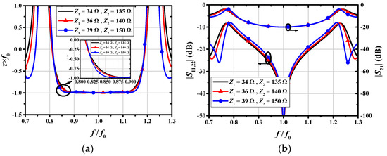
Figure 5.
The performance at different Z1 and Z2 values with fixed τg × f0 = −1.0 and |S21| = −20 dB at f0. (a) τg × f0; (b) S−parameters.
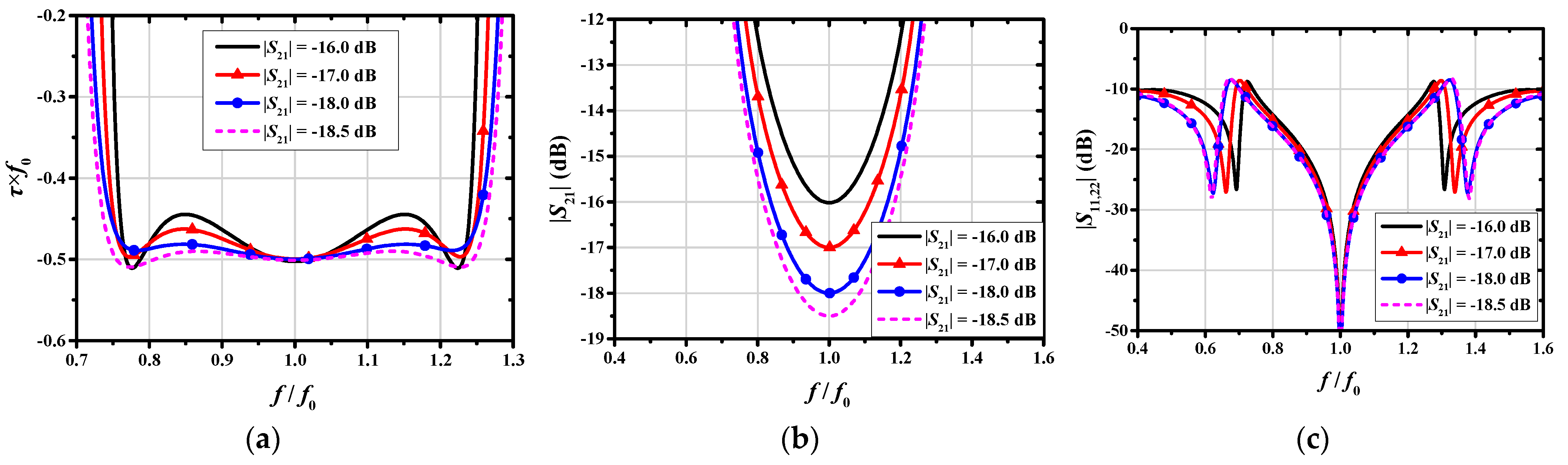
It is worthy to note the effect of different values for |S21| on the entire circuit performance when the Z1, Z2 and NGD values are fixed at f0. As can be seen in Figure 6, when |S21| decreases from −16 dB to −18.5 dB, the ripple of τg × f0 near the center frequency f0 also decreases. Therefore, the NGD time, |S21| and flat-NGD bandwidth need to be considered comprehensively.
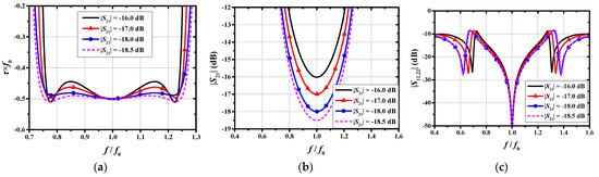
Figure 6.
The performance with different |S21| values with fixed Z1 = 60 Ω, Z2 = 150 Ω and τg × f0 = −0.5 at f0. (a) τg × f0; (b) |S21|; (c) |S11,22|.
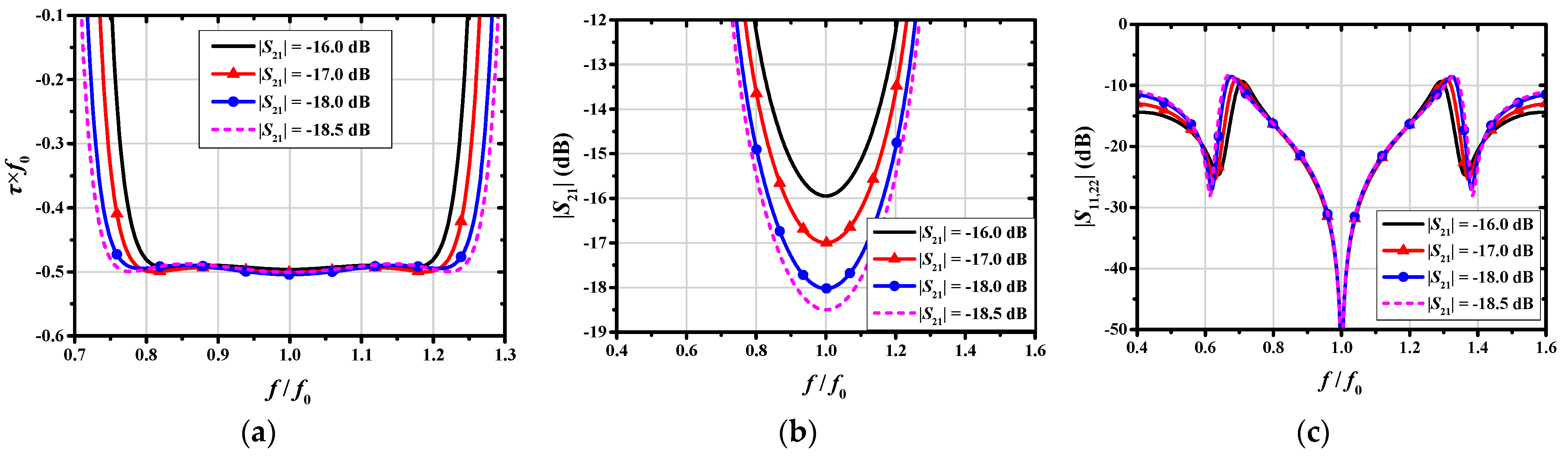
For the discussion of the maximum flat-NGD bandwidth, Figure 7 gives the τg × f0 and S-parameters under the same |S21|with that in Figure 6. To obtain the maximum flat-NGD bandwidth, the values of Z1 and Z2 are changed in Figure 7. It can be seen that the maximum flat-NGD bandwidth increases with the |S21| decreases.
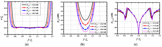
Figure 7.
The performance with different |S21| values with fixed τg × f0 = −0.5 at f0. (a) τg × f0; (b) |S21|; (c) |S11,22|.
For convenience, a simple design process of the proposed circuit is summarized as follows.
Step 1: Determine the desired |S21| and NGD time at the center frequency f0.
Step 2: Choose a proper Z2 according to Figure 3 and Figure 5. Then, calculate R, P and Q using Equations (16)–(23).
Step 3: Select an appropriate Z1 according to Figure 4 and Figure 5. Then, calculate Z0e and Z0o using Equations (24)–(26).
Step 4: If the flatness of GD is not enough after the first three steps, return to Step 2 and adjust Z1 and Z2 to other potential values.
Step 5: If the flatness of GD is not enough or the maximum flat-NGD bandwidth is not satisfied after the first four steps, return to Step 1 and adjust |S21|.
3. Experimental Verification
To confirm the design concept, a compact broadband NGDC is designed at the center frequency f0 = 1.0 GHz with GD = −0.5 ns. Using the design procedures in Section 2, the electrical parameters can be obtained as Z1 = 59 Ω, Z2 = 150 Ω, Z0e = 74.6 Ω, Z0o = 39.1 Ω, R = 52 Ω. Then the flat-NGDC is implemented on the substrate with a thickness of 1.0 mm, with a dielectric constant of 2.65 and a loss tangent of 0.003. The layout of the proposed compact broadband NGDC is given in Figure 8a. After optimizing by HFSS EM 2018 software, the final physical dimensions are w1 = 2.0 mm, l11 = 7.0 mm, l12 = 23.0 mm, l13 = 5.0 mm, w2 = 0.2 mm, l21 = 6.5 mm, l22 = 17.8 mm, l23 = 6.9 mm, w = 2.0 mm, s = 0.2 mm, l = 49.0 mm, wp = 1.8 mm, lp = 5.0 mm, with R = 50 Ω. The photo of the fabricated compact broadband NGDC is given in Figure 8b. The overall circuit dimension is 29.4 mm × 58.1 mm (0.14 λg × 0.29 λg, where λg is the guided wavelength of 50-Ω TLs at the center frequency). The measurements are completed by an AV3565A network analyzer manufactured in China Electronics Technology Group Corporation 41st Research Institute, Beijing, China.
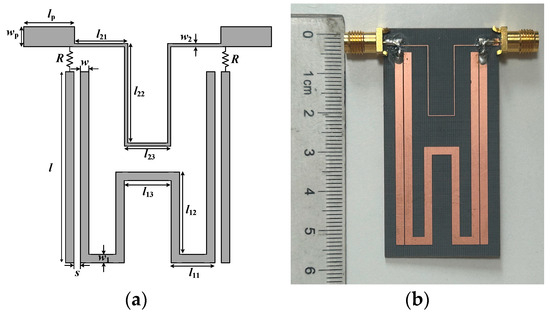
Figure 8.
The proposed compact broadband NGDC. (a) Layout; (b) Photograph.
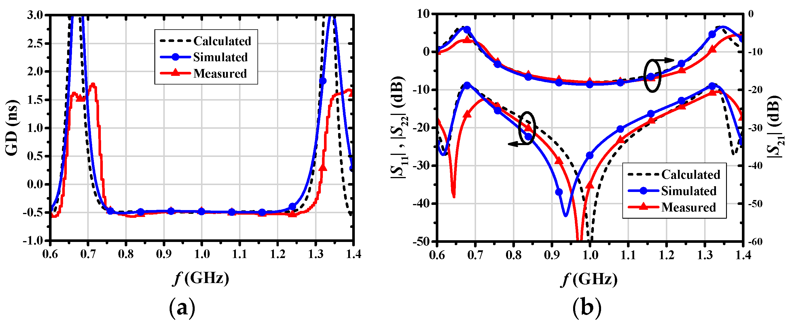
Figure 9 shows the measured GD and S-parameters, along with the simulated and calculated results for comparison. It can be seen from Figure 9a that the calculated, simulated and measured flatness and GD (f0) are basically consistent. And, the measured flat-NGD bandwidth is slightly offset directly from the simulated one. A relatively good consistency for calculated, simulated and measured |S21| has been shown in Figure 9b. The calculated |S11| and |S22| at f0 is minimized, which means the port is matching ideally. And, the simulated and measured |S11|, |S22| has a slight frequency shift, but good port matching characteristics are implemented within the flat-NGD bandwidth. The differences between the measured results and the simulated results are due to the inaccuracy of the substrate parameters.
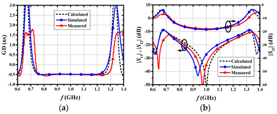
Figure 9.
Calculated, simulated and measured results of the proposed compact broadband NGDC. (a) GD; (b) S−paremeters.
The measured GD, |S21| and|S11| at f0 are −0.48 ns, −18 dB and −35 dB, respectively. The measured NGD bandwidth of the presented NGDC is 569 MHz (56.9%) over 741 to 1310 MHz; meanwhile, the flat-NGD bandwidth is 509 MHz (50.9%) over 766 to 1275 MHz. And, the input/output return loss is better than 13 dB within the flat-NGD bandwidth. The insertion loss bandwidth, which is defined as the 3-dB variation from the center frequency |S21|, is 439 MHz (43.9%) over 800 to 1239 MHz. The comparisons of the presented NGDC with precious works are given in Table 1. Compared with [21,23,24], they have a close center frequency and NGD time, but the presented NGDC has the largest flat-NGD bandwidth with a moderate IL. For a better comparison, the figure of merits (FOM1 and FOM2) have been used, which are defined as [22]

Table 1.
Performance comparison between the proposed compact broadband NGDC and previous flat-NGD circuits.
It can be seen from Table 1 that the proposed NGDC has a larger FOM1 and FOM2 than [18,19,20,21,22,23,24] with a moderate GD ripple. Moreover, the circuit size of the proposed NGDC is the smallest.
4. Conclusions
In this paper, a compact broadband NGDC has been proposed, and the design equations at the center frequency have been simplified. The free variables (Z1 and Z2) used to achieve the enhancement of the GD flatness have been discussed. An NGDC with a size of 0.14 λg × 0.29 λg has been designed, simulated, fabricated and measured. A very good agreement is confirmed by simulation and measurement results. Compared to the existing flat-NGDCs, the presented NGDC has a larger FOM1 and FOM2 with moderate GD ripple and the smallest circuit size.
Author Contributions
Conceptualization, Y.M.; methodology, Y.M.; software, Y.M.; validation, Y.M. and A.Y.; formal analysis, Y.M.; investigation, Y.M. and A.Y.; resources, Y.M., P.L. and A.Y.; data curation, Y.M. and Z.L.; writing—original draft preparation, Y.M.; writing—review and editing, Y.M. and A.Y.; supervision, P.L. and Z.L.; project administration, Y.M.; funding acquisition, Y.M. All authors have read and agreed to the published version of the manuscript.
Funding
This research was funded by Special Funds for Basic Scientific Research Expenses of Undergraduate Universities in Liaoning Province, grant number LJBKY2024069.
Data Availability Statement
The original contributions presented in the study are included in the article, further inquiries can be directed to the corresponding author.
Conflicts of Interest
The authors declare no conflicts of interest.
References
- Ahn, K.-P.; Ishikawa, R.; Honjo, K. Low noise group delay equalization technique for UWB InGaP/GaAs HBT LNA. IEEE Microw. Wirel. Components Lett. 2010, 20, 405–407. [Google Scholar] [CrossRef]
- Mirzaei, H.; Eleftheriades, G.V. Arbitrary-angle squint-free beamforming in series-fed antenna arrays using non-Foster elements synthesized by negative-group-delay networks. IEEE Trans. Antennas Propag. 2015, 63, 1997–2010. [Google Scholar] [CrossRef]
- Baloglu, O.; Cicekoglu, O.; Herencsar, N. Single CFOA-based active Negative Group Delay circuits for signal anticipation. Eng. Sci. Technol. Int. J. 2023, 48, 101590. [Google Scholar] [CrossRef]
- Ravelo, B.; Wan, F.; Nebhen, J.; Rahajandraibe, W.; Lalléchère, S. Resonance effect reduction with bandpass negative group delay fully passive function. IEEE Trans. Circuits Syst. II Express Briefs 2021, 68, 2364–2368. [Google Scholar] [CrossRef]
- Yuan, A.; Fang, S.; Wang, Z.; Liu, H. A Novel Multifunctional Negative Group Delay Circuit for Realizing Band-Pass, High-Pass and Low-Pass. Electronics 2021, 10, 1742. [Google Scholar] [CrossRef]
- Nako, J.; Psychalinos, C.; Elwakil, A.; Maundy, B. Power-Law Negative Group Delay Filters. Electronics 2024, 13, 522. [Google Scholar] [CrossRef]
- Mirzaei, H.; Eleftheriades, G.V. Realizing non-Foster reactive elements using negative-group-delay networks. IEEE Trans. Microw. Theory Tech. 2013, 61, 4322–4332. [Google Scholar] [CrossRef]
- Zhang, T.; Yang, T. A novel fully reconfigurable non foster capacitance using distributed negative group delay networks. IEEE Access 2019, 7, 92768–92777. [Google Scholar] [CrossRef]
- Wan, F.; Miao, X.; Ravelo, B.; Yuan, Q.; Cheng, J.; Ji, Q.; Ge, J. Design of multi-scale negative group delay circuit for sensors signal time-delay cancellation. IEEE Sens. J. 2019, 19, 8951–8962. [Google Scholar] [CrossRef]
- Ravelo, B.; Wan, F.; Ge, J. Anticipating actuator arbitrary action with a low-pass negative group delay function. IEEE Trans. Ind. Electron. 2021, 68, 694–702. [Google Scholar] [CrossRef]
- Chaudhary, G.; Jeong, Y.; Lim, J. Microstrip line negative group delay filters for microwave circuits. IEEE Trans. Microw. Theory Tech. 2014, 62, 234–243. [Google Scholar] [CrossRef]
- Wang, Z.; Cao, Y.; Shao, T.; Fang, S.; Liu, Y. A negative group delay microwave circuit based on signal interference techniques. IEEE Microw. Wirel. Components Lett. 2018, 28, 290–292. [Google Scholar] [CrossRef]
- Ravelo, B.; Wan, F.; Li, N.; Xu, Z.; Thakur, P.; Thakur, A. Diakoptics modelling applied to flying bird-shape NGD microstrip circuit. IEEE Trans. Circuits Syst. II Express Briefs 2021, 68, 637–641. [Google Scholar] [CrossRef]
- Liu, Z.; Zhang, J.; Lei, X.; Gao, J.; Xu, Z.; Li, T. Negative Group Delay Metamaterials Based on Split-Ring Resonators and Their Application. Electronics 2023, 12, 1064. [Google Scholar] [CrossRef]
- Ravelo, B.; Le Roy, M.; Perennec, A. Application of negative group delay active circuits to the design of broadband and constant phase shifters. Microw. Opt. Technol. Lett. 2008, 50, 3078–3080. [Google Scholar] [CrossRef]
- Qiu, L.; Wu, L.; Yin, W.; Mao, J. A filter with equal-ripple negative group delay. In Proceedings of the 2018 IEEE Radio and Wireless Symposium, Anaheim, CA, USA, 15–18 January 2018. [Google Scholar]
- Shao, T.; Fang, S.; Wang, Z.; Liu, H. A compact dual-band negative group delay microwave circuit. Radioengineering 2018, 27, 1070–1076. [Google Scholar] [CrossRef]
- Wu, Y.; Wang, H.; Zhuang, Z.; Liu, Y.; Xue, Q.; Kishk, A.A. A novel arbitrary terminated unequal coupler with bandwidth-enhanced positive and negative group delay characteristics. IEEE Trans. Microw. Theory Tech. 2018, 66, 2170–2184. [Google Scholar] [CrossRef]
- Wang, H.; Wu, Y.; Wu, Z.; Wang, W.; Liu, Y. Compact arbitrary terminated power divider with bandwidth-enhanced negative group delay characteristics. Int. J. Circuit Theory Appl. 2019, 47, 909–916. [Google Scholar] [CrossRef]
- Chaudhary, G.; Jeong, Y. Arbitrary terminated negative group delay circuit using signal interference concept. Int. J. RF Microw. Comput. Aided Eng. 2020, 30, e22341. [Google Scholar] [CrossRef]
- Meng, Y.; Wang, Z.; Fang, S.; Shao, T.; Liu, H.; Chen, Z. Group delay flatness and bandwidth enhancement of wideband negative group delay microwave circuit. Int. J. RF Microw. Comput. Aided Eng. 2020, 30, e22443. [Google Scholar] [CrossRef]
- Wang, Z.; Meng, Y.; Fang, S.; Liu, H. Wideband flat negative group delay circuit with improved signal attenuation. IEEE Trans. Circuits Syst. II Express Briefs 2022, 69, 3371–3375. [Google Scholar] [CrossRef]
- Gu, T.; Wan, F.; Chen, J.; Ravelo, B.; Zhao, X. Compact and wideband flat negative group delay circuit investigation. IEEE Trans. Circuits Syst. II Express Briefs 2023, 70, 1916–1920. [Google Scholar] [CrossRef]
- Zheng, Y.; Wang, W.; Wu, Y. Planar coupled-line-based flat negative group delay microwave circuit with size reduced and bandwidth enhanced. IEEE Trans. Circuits Syst. II Express Briefs 2023, 70, 4339–4343. [Google Scholar] [CrossRef]
- Hee-Ran, A. Asymmetric Passive Components in Microwave Integrated Circuits, 1st ed.; John Wiley & Sons: Hoboken, NJ, USA, 2006; pp. 66–77. [Google Scholar]
Disclaimer/Publisher’s Note: The statements, opinions and data contained in all publications are solely those of the individual author(s) and contributor(s) and not of MDPI and/or the editor(s). MDPI and/or the editor(s) disclaim responsibility for any injury to people or property resulting from any ideas, methods, instructions or products referred to in the content. |
© 2024 by the authors. Licensee MDPI, Basel, Switzerland. This article is an open access article distributed under the terms and conditions of the Creative Commons Attribution (CC BY) license (https://creativecommons.org/licenses/by/4.0/).