Article

An Adaptive High-Efficiency LED Backlight Driver

School of Physical and Electronic Sciences, Changsha University of Science and Technology, Changsha 410114, China
*
Author to whom correspondence should be addressed.
Electronics 2024, 13(15), 3057; https://doi.org/10.3390/electronics13153057
Submission received: 22 June 2024 / Revised: 25 July 2024 / Accepted: 30 July 2024 / Published: 2 August 2024

Abstract

:
An adaptive high-efficiency light-emitting Diode (LED) backlight driver scheme has been proposed to address the issue of additional power loss caused by LED forward voltage variation. In this scheme, the peak current and the duty cycle of each LED channel are adjusted separately through an adaptive control algorithm to minimize the voltage drop on the linear current regulator (LCR) of each LED channel to reduce the excessive power loss in each LED channel and enhance the total power efficiency. A linear current regulator, suitable for adaptive control, is designed on a 0.18 μm 5V complementary metal-oxide-semiconductor (CMOS) process. Simulation results demonstrate that the linear current regulator can achieve a linearly adjustable channel current ranging from 0 to 48 mA with a current resolution of 0.2 mA. Across different process corners and temperatures, the maximum error for the full current range is less than 0.1%. The core area of chip layout is about 0.1 mm2. The complete driver prototype comprises the LCR chips, external power MOS transistors, digital module, and LED chains. The test results show that the power loss of the linear current regulator has been significantly reduced, and the power efficiency of each LED channel has been measured at around 98.1%.

1. Introduction

Light-emitting diodes (LEDs) have been widely adopted as backlight sources for liquid crystal display (LCD) devices and other applications. Compared to traditional light sources, LEDs offer significant advantages such as high efficiency, excellent color stability, high reliability, long lifespan, compact size, and environmental safety [1,2,3,4]. Since the brightness of LED is proportional to its current, an efficient and accurate driver circuit is essential in LED backlight applications to achieve precise brightness control. Additionally, parallel LED channels (LED chains) are always employed to ensure sufficient coverage [5,6]. A traditional LED backlight driver is primarily composed of a boost converter, parallel LED channels, and corresponding linear current regulators (LCRs). The boost converter provides sufficient voltage to turn on all LEDs in each channel, and the LCR regulates the current for each channel to control brightness [7,8,9]. As an important area of power management application, the design of LED backlight drivers has always been a popular research focus for numerous universities and research institutions worldwide. The objective is to optimize system performance through innovative circuit designs and system architectures, with an emphasis on metrics such as system efficiency [10,11,12,13,14,15], dimming ratio [16,17,18,19,20], and current accuracy [21,22,23,24,25].
Due to process variations, aging effects, and temperature changes, LEDs of the same type can exhibit different forward voltage, resulting in significant voltage discrepancies across different LED channels. Consequently, it is necessary to introduce a certain amount of voltage headroom to ensure correct functionality under various working conditions. However, this also leads to increased power loss and deteriorated power efficiency [26,27]. A digital control mechanism based on an R-DAC was proposed in [28] to address the problem of increased power loss due to excessive voltage. A comparison between the voltage on the LCR and a pre-set reference voltage is conducted, which drives the adjustment of the feedback voltage of the DC–DC boost converter via a digital-to-analog converter (DAC). The boost converter’s output is then adjusted to maintain the LCR voltage at a fixed level. In [29], an adaptive reference tracking technique was proposed, using a “Minimum Voltage” circuit and a 3-bit adjustable resistor as a feedback resistor to adjust the output of the boost converter. The accuracy of the output voltage is influenced by the precision and adjustment range of the resistor. In [30,31,32,33,34], through “Minimum Voltage Selector” or “Lowest channel selector”, the minimum LCR voltage among channels is detected and used to dynamically adjust the duty cycle of the boost converter’s switch signal and change the boost converter’s output. In [35,36], diodes are used to select the minimum LCR voltage, a method that is not easily implemented in standard CMOS processes. In [2], the advantages and disadvantages of various LED driver topologies were analyzed, and future research directions were identified.
In general, for most existing solutions, the main strategy is to adjust the boost converter’s output voltage to reduce the excessive voltage on the LCR, thereby reducing losses and improving efficiency. However, for multi-channel configuration, due to the inter-channel differences, it is more effective to optimize each channel separately to further reduce loss and enhance efficiency. In this paper, we propose an adaptive high-efficiency LED backlight driving scheme that addresses the issue of inter-channel differences. Both linear current regulation and pulse width modulation (PWM) are employed for each channel. Through linear current regulation, the channel current is adjusted, and the voltage on the LCR in each channel is minimized to a predefined fixed value. Subsequently, through pulse width modulation, the duty cycle of channel current is adjusted, calibrating the average current of each channel to the same level. This strategy ensures that each LED channel operates with minimal loss, thereby maximizing efficiency.
The structure of the remaining parts of this article is as follows: Section 2 elaborates on the adaptive control technology designed in this paper. Section 3 discusses and analyzes the simulation results and test results of the proposed adaptive high-efficiency LED backlight driver. Section 4 concludes the paper.

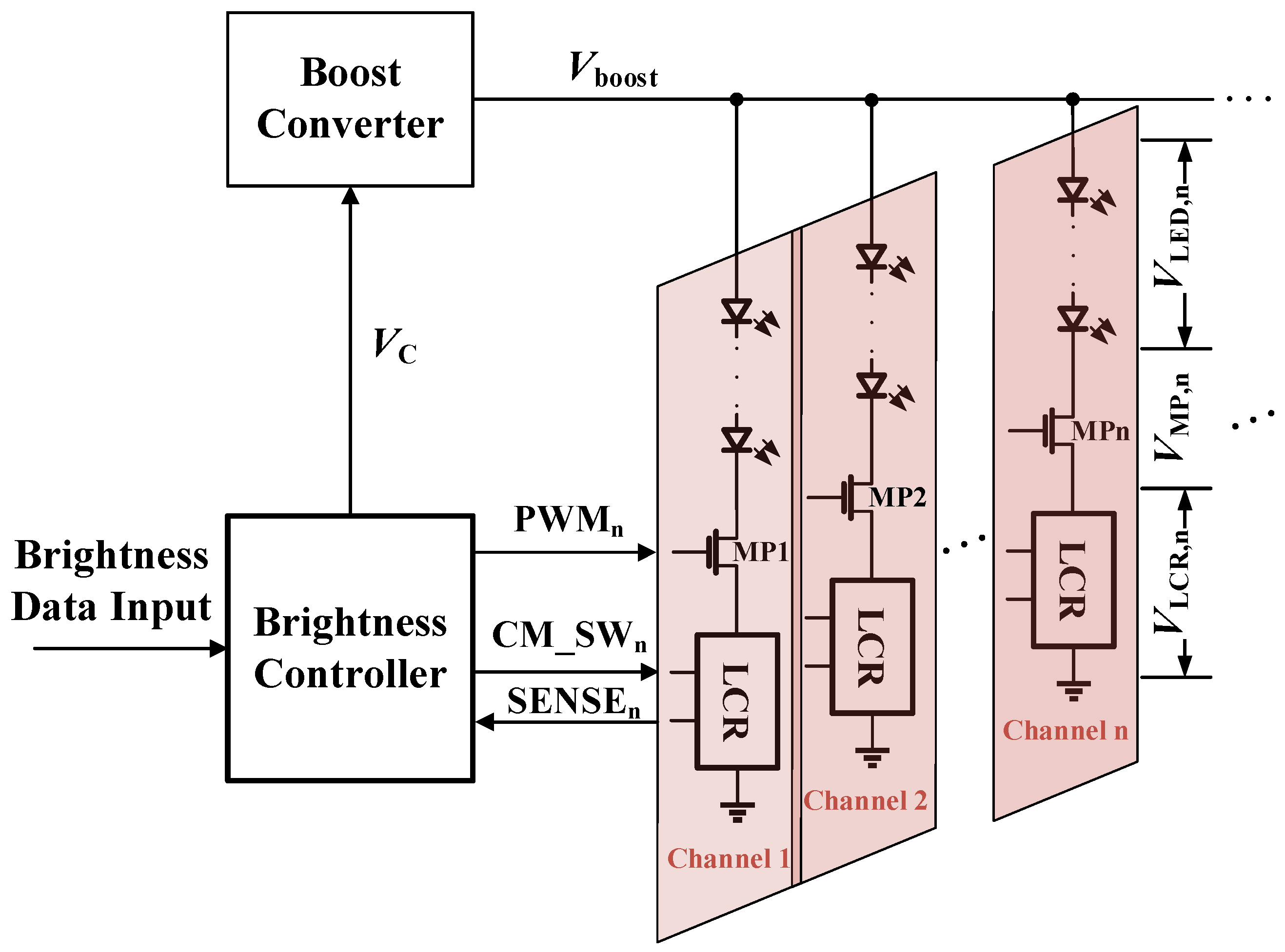
2. Adaptive Control Technique

2.1. Principle of Adaptive Control

Figure 1 illustrates the structure of the proposed adaptive high-efficiency LED backlight driver, which comprises a brightness controller, a boost converter, and several LED channels. Each LED channel consists of an LED chain, an LCR, and a high-voltage MOS transistor acting as a switch for duty cycle control. The brightness controller includes a 9-bit R-DAC to produce VC, which serves as a voltage reference and determines the output of the boost converter Vboost. The SENSE signal indicates whether the LCR is on the right status. The brightness controller monitors SENSE of each channel and generates VC, PWM, and CM_SW signals following a specific algorithm and steps. CM_SW and PWM are multi-bit digital signals that control the peak current and the duty cycle of the channel, respectively. This process ensures that each LED channel operates at a high-efficiency state.
From the figure, for channel n, there exists a voltage relationship as
V b o o s t = V L E D , n + V M P , n + V L C R , n
where VLED is the voltage across the LED chain or the summation of the forward voltage of each LED. VMP is the source-drain voltage of the high-voltage MOS transistor MP, and VLCR denotes the LCR voltage. The “n” in subscript indicates channel n, which applies to all symbols in this paper. If the adaptive control is disabled and the LED channel is not in the optimal state, there will be an excessive portion in the LCR voltage, which can be expressed as follows:
V LCR , n = V LCR _ min + V LCR _ exc , n
where VLCR_min is the minimum required LCR voltage to ensure proper operation, that is to say, the output transistor in the LCR works properly and maintains accurate output current. VLCR_exc represents the excessive portion of the LCR voltage. For one channel, the power loss can be calculated by
P loss , n = I ave , n × V loss , n = I ave , n × ( V LCR , n + V MP , n )
where Iave,n is the average current, which is determined by the peak current Ipeak,n and the current duty cycle δn. Vloss,n is the summation of VLCR,n and VMP,n. If the on-resistances of the high-voltage MOS transistors are low enough, VMP has limited impact on Ploss. Because VMP and VLCR_min are prerequisite to maintain the MOS and LCR operate appropriately, the excessive power loss is defined as
P loss _ exc , n = I ave , n × V LCR _ exc , n

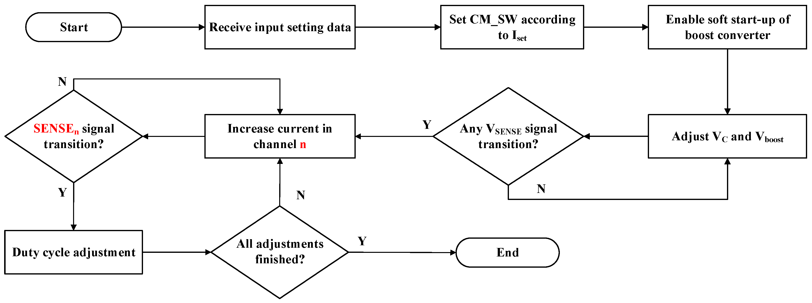
2.2. Adaptive Control Process

An adaptive control process suitable for multi-channel LED drivers is designed to reduce excessive power loss caused by the excessive voltage. At system startup, the brightness controller initiates an initialization process, during which the peak current and duty cycle of each LED channel are individually set to achieve uniform brightness and simultaneously minimize excessive power loss. After the initialization phase, the brightness controller transitions into the tracking phase, where it continuously monitors the status of the LCR. The peak current and duty cycle settings are then adjusted accordingly to accommodate fluctuations in power supply, temperature, and other factors.
Figure 2 shows the flowchart of the initialization phase. Firstly, the brightness input data, including the nominal peak current Iset and the duty cycle δset, are loaded into the brightness controller. Subsequently, the LCR current of each channel is set to Iset via the CM_SW signal. The brightness controller then begins to increase VC, causing Vboost to decrease accordingly. Meanwhile, the brightness controller simultaneously monitors the status signal SENSE from each channel. Once all SENSE signals change from 0 to 1, the increase in VC stops. At this point, the peak currents of all channels have reached the preset value of Iset, and there is always one channel, assumed to be channel k, whose SENSE signal is the last to change.
Next, a peak current adjustment step is carried out sequentially on all channels except channel k. The brightness controller attempts to increase the channel current by providing a new CM_SW setting. If SENSE remains at 1, the brightness controller continues this process. However, if SENSE changes from 1 to 0, the brightness controller reverts to the previous CM_SW setting, concluding the adjustment process for that channel. The corresponding channel then has a new peak current. The brightness controller proceeds to conduct the adjustment process for the subsequent channel. Once all current adjustments are completed, the voltage on each LCR approaches VLCR_min, and the excess component has been minimized.
Finally, in order to ensure the same brightness, each LED channel needs to have the same average current. Therefore, the duty cycle of channel n (δn) is adjusted by the brightness controller as follows:
δ n = δ s e t × I s e t I peak , n
where Ipeak,n is the peak current of n-th LED channel after adjustment process as described above. δset and Iset represent the initial duty cycle and peak current, respectively. It is worth noting that, according to Equation (4), the average current remains unchanged.
Through the aforementioned process, the peak current Ipeak,n and duty cycle δn for each LED channel are adjusted, thereby minimizing additional power consumption resulting from excessive voltage. The adjusted average current closely aligns with the initially set average current. Given that the brightness output of LEDs correlates directly with their current, the adaptive control method ensures that the brightness levels across all LED channels remain consistent. Upon entering the tracking phase, the main principle resembles that of the initialization phase. Both of them combine the adjustment of peak current and duty cycle and will not be described in detail in this article.

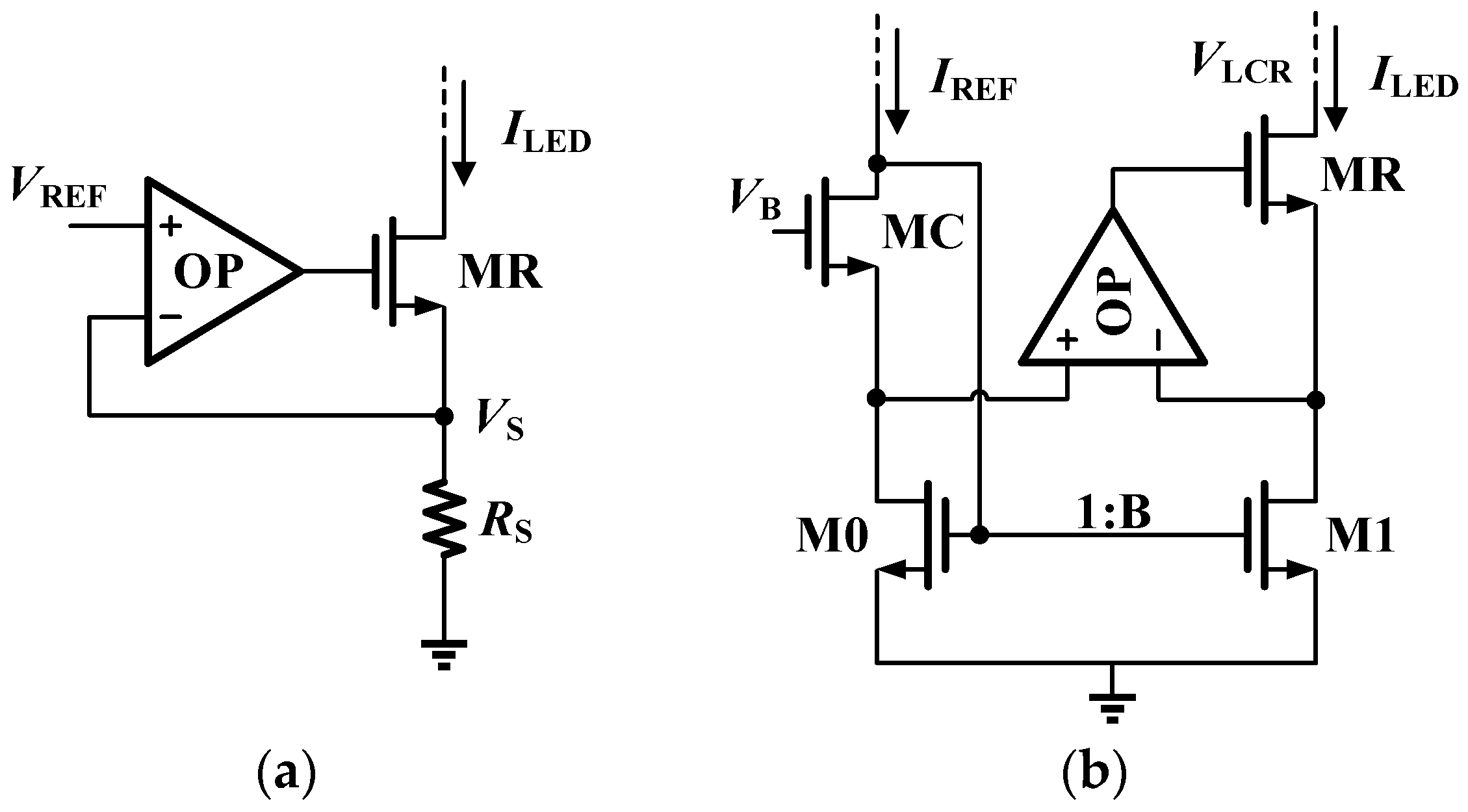
2.3. Linear Current Regulator

Because LED brightness is directly influenced by its current, precise brightness control necessitates accurate current regulation. In many LED backlight driver solutions, an LCR is typically employed for generating and controlling the LED current. Figure 3 illustrates two typical LCR circuit configurations [37]. A key design objective for LCR circuits is achieving high current accuracy. In Figure 3a, the operational amplifier and the transistor M1 form a negative feedback, ensuring that VS equals to VREF. Consequently, the output current ILED is VREF/RS. Clearly, the accuracy of RS directly affects ILED’s precision. It is important to note that the driving currents for backlight LEDs are generally substantial. In this paper, the maximum driving current is designed to be 48 mA. Additionally, to minimize power loss, VS or VREF should be kept as low as possible, necessitating a small RS to achieve high currents. However, excessively small RS can significantly enhance the negative impact of circuit parasitics on output current accuracy.
Figure 3b depicts another type of LCR. In this configuration, the output current ILED is not directly generated as in Figure 3a, but through current mirroring. In this structure, ILED is determined by B × IREF, where IREF is a reference current and B is the current mirror ratio, which is defined by the size ratio of transistor M1 to M0. The operational amplifier (OP) plays a crucial role by ensuring that transistors M1 and M0 have the same VDS, thereby guaranteeing accurate current mirroring.
Actually, M0 and M1 can work in the linear region instead of the saturation region by lowing VB, thereby reducing VDS, which helps to lower VLCR and reduce excessive power [38]. The classic drain current expression for MOS transistors working in the linear region is
I D = 1 2 μ C OX ( W L ) [ 2 ( V GS V TH ) V DS ] V DS
The transistor can now be approximately equivalent to a linear resistor. As mentioned above, due to the effect of OP, the VDS of M0 and M1 are kept at the same. Then the drain current of M0 and M1 has a relationship as
I D , M 0 I D , M 1 = ( W / L ) M 0 ( W / L ) M 1 = 1 B
Clearly, accurate current mirroring is guaranteed.
Based on the circuit structure shown in Figure 3b, an improved LCR for adaptive control was designed as depicted in Figure 4. The main difference from the circuit in Figure 3b is the introduction of operational amplifier OP2. OP2, in conjunction with transistor M0, forms a negative feedback loop ensuring that the source-drain voltage VDS of M0, denoted as VA in the figure, remains equal to VREF. By adjusting VREF, the source-drain voltage VDS of M0 can be precisely controlled. The advantage of the design is that it mitigates the impact of process variations and facilitates accurate parameter control. When VREF is low, transistor M0 operates in the linear region. Transistors M1, M2, …, MN serve as current mirror transistors corresponding to M0, each having the same size. The decoder determines whether each mirror transistor is activated or deactivated based on the binary control word CM_SW, thereby adjusting the total output current. When a mirror transistor’s gate is connected to VCOM, it turns on; when connected to ground, it turns off. OP1 functions similarly to OP in Figure 3b, ensuring that the voltage at node D (denoted as VD) matches VA, thereby maintaining accurate current mirroring. The comparator COMP works as a simple circuit state detector with VCOM set to 2.5 V in this design. OP1 is a high-gain operational amplifier with a gain-boosting output structure [39], while OP2 is an operational amplifier with a rail-to-tail class-AB output stage [40].
When Vboost is sufficiently high, even after accounting for the voltage drop across the LED chain, there remains enough VLCR to ensure the proper operation of the LCR, allowing ILED to reach or maintain its set value. At this condition, the gate voltage of the transistor MR is approximately 1.86 V (VGS,MR + VREF) according to the simulation results at the typical process corner, and SENSE stays at 1. If Vboost decreases or if ILED increases and makes the forward voltage of the LED chain increase, VLCR will correspondingly decrease. However, as long as transistor MR remains effective, the LCR can continue to function normally. If VLCR decreases further and pushes transistor MR into deep linear region, VG must be increased to counteract the impacts of the decreasing VLCR. When VG exceeds VCOM, the output of the comparator changes state, and SENSE switches to 0. This indicates that the LCR may no longer be able to maintain or achieve the set ILED.
All mirror transistors have the same size, and each transistor has a size ratio of B:1 with M0. The LED current can be determined by the following equation:
I LED = N × B × I REF
where N is the number of activated mirror transistors and determined by CM_SW. IREF is the reference current generated by the external bias circuit. It should be noted that the output current ILED of the LCR actually forms the aforementioned peak current Ipeak.
Even on the same chip, there is a certain degree of process variation, which primarily affects the device size and characteristic parameters, leading to inaccuracies or mismatches in the current mirroring. Considering the influence of the width-to-length ratio (W/L) and the threshold voltage (Vth), the current change caused by process variation can be expressed as follows:
Δ I = I ( W / L ) Δ ( W / L ) + I V t h Δ V t h
The current mismatch is usually defined as the rate of change of current. Assuming no correlation between different influencing factors, it can be expressed as:
Δ I I = 1 I I ( W / L ) Δ ( W / L ) + I V t h Δ V t h
If the transistor operates in the saturation region, according to the corresponding drain current formula, the current mismatch is
Δ I I = Δ ( W / L ) ( W / L ) + 2 Δ V t h ( V GS V t h )
While if the transistor operates in the linear region, according to the corresponding drain current formula, the current mismatch becomes
Δ I I = Δ ( W / L ) ( W / L ) + 2 Δ V t h 2 ( V GS V t h ) V DS
Comparing the two formulas above, it can be seen that the impact of size variation on current mismatch is the same in both the linear and the saturation regions. However, the impact of threshold voltage variation is smaller in the linear region, indicating that it is possible to achieve lower current mismatch in the linear region.

3. Simulation and Measurement Results

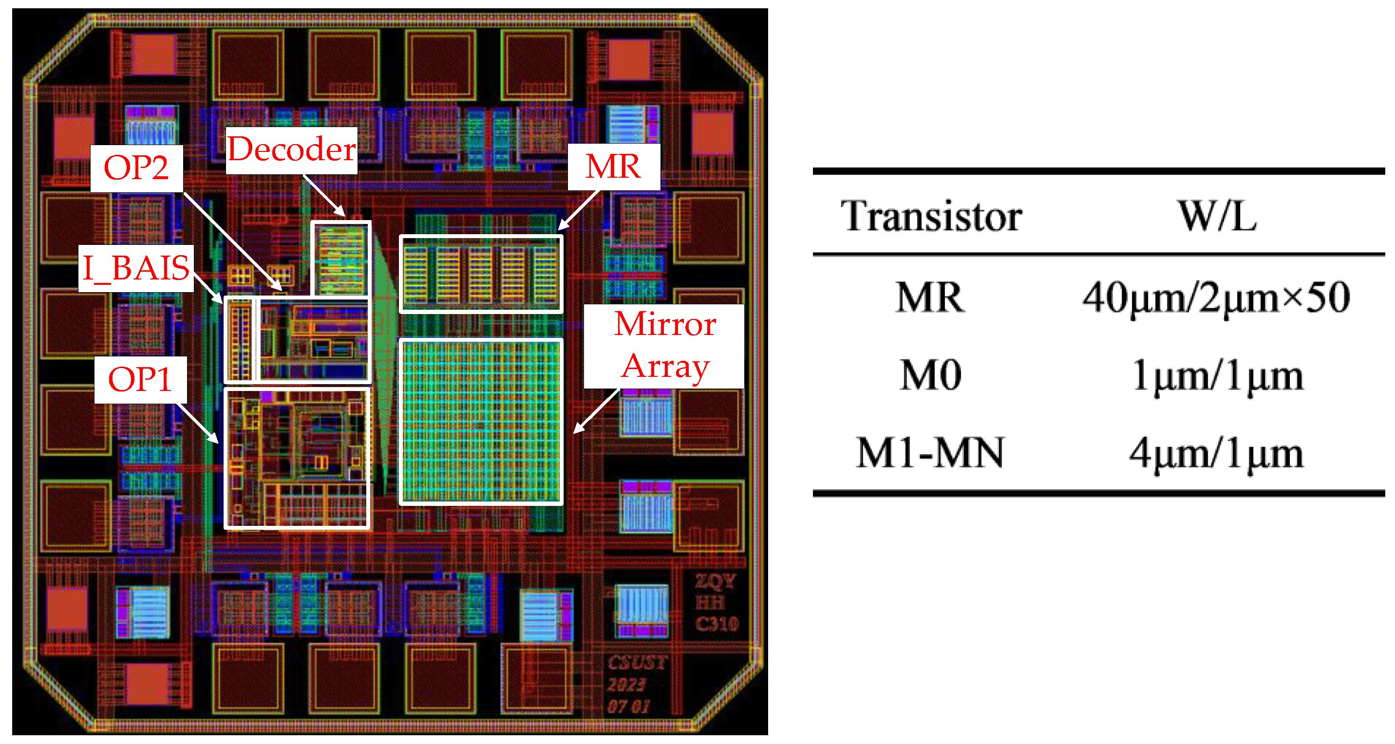
3.1. System and Chip Design

Based on Figure 2, this paper constructs and validates a three-channel adaptive LED driver, with each channel comprising 6 LEDs. A boost converter chip, specifically the TPS61046 from Texas Instruments, is used. The LCR is designed using a 0.18 μm complementary metal-oxide-semiconductor (CMOS) 5 V process. Since this process does not support high-voltage devices, external MP transistors are employed. Ideally, if a BCD process is available, these MP transistors could be integrated directly onto the chip. Additionally, further integration of the brightness controller is envisioned for achieving a monolithic integrated driver chip, which is a planned future work. In circuit simulation, PSPICE models are employed for the boost converter, LEDs, and MP transistors. The on-voltage parameter in the PSPICE model for LED is intentionally adjusted to introduce differences between channels. Specifically, for channel 3, the LED on-voltage is set to 3.20 V, representing a typical value. For channels 1 and 2, the parameters are adjusted to 2.73 V and 2.76 V, respectively. As described earlier, the minimum value of Vboost is dictated by the VLED of channel 3. The brightness controller is implemented using Verilog HDL and runs at the frequency of 100 MHz. The frequency of the PWM signal is 10 KHz. The entire circuit runs in a mixed-signal simulation mode to verify the adaptive control process and assess the performance of the LCR.
In consideration of current control range and resolution, the size of M0 in the LCR is chosen to be 1 μm/1 μm, and its ratio to the mirror transistor is set to be 1:4. There are 240 current mirror transistors in total. The reference current IREF is set to be 50 μA, resulting in a unit output current of 200 μA and a maximum output current of 48 mA. The size of MR is chosen to be 40 μm/2 μm × 50. The overall layout of the LCR circuit is shown in Figure 5. All mirror transistors and their corresponding control switches are arranged in the form of a 15 × 16 array. The core area is only 325 μm × 310 μm, while the entire area, including pads, is 700 μm × 720 μm. The key transistor sizes are also summarized in Figure 5.

3.2. Simulation Results

Figure 6 depicts the simulated output characteristics of the LCR under different process corners and temperatures. It can be seen that when the output current LCR ranges from 0 mA to 48 mA, it demonstrates good linearity under different operating conditions. Specifically, at an output current setting of 20 mA, the maximum current deviation is 13 μA, resulting in a current error of less than 0.1%. Overall, the LCR exhibits good current linearity and accuracy within the specified current range.
Figure 7 depicts the voltage waveform at several essential nodes during the adaptive process. SENSE1, SENSE2 and SENSE3 represent the SENSE signals of the corresponding channels. T0 denotes the soft start phase of the boost converter. Upon power-on, the output of the boost converter Vboost gradually reaches a preset value after a period of time. This preset value is the minimum voltage for the circuit to operate properly under various working conditions and is set to 25.19 V in this design. As Vboost increases, the SENSE signals of each channel sequentially transition to 0. T1 marks the Vboost adjustment phase. During this time, the brightness controller gradually increases VC, leading to a corresponding decrease in Vboost. It can be seen that when Vboost reaches 21.52 V, SENSE3 transitions to 1, indicating a change in the status of channel 3. Finally, VC stays at 0.33 V, and Vboost is stabilized at 21.62 V. T2 marks the current regulation phase, during which the current of channel 1 (channel 2) increases. When SENSE1 (SENSE2) transitions to 1, it indicates that the status of channel 1 (channel 2) has changed. The current regulation of channel 1 (channel 2) is ceased, and the duty cycle of channel 1 (channel 2) is set according to Equation (4). T3 represents the normal working phase, which is also called the continuous tracking phase, and SENSE signals are dynamically kept at 0.
Figure 8 illustrates the current waveform in each channel. Initially, the peak current value of each channel is set to 20 mA, with a default duty cycle of 100%. During the early stage of T0, Vboost has not been fully established, and all LEDs are in the off state, resulting in zero current in each channel. Because the LEDs in channel 3 have the largest forward voltage, the current in channel 3 is the last rising to the set value, consistent with the timing of SENSE signals in Figure 7. Following the completion of the Vboost adjustment phase, the current regulation phase starts. It can be seen that the peak currents in channel 1 and channel 2 are increased to 24.2 mA and 23.2 mA, respectively, with the corresponding duty cycles adjusted to 82.6% and 86.2%, ensuring uniform average currents across the three channels. When the normal working phase begins, the brightness controller will continuously monitor the state of the LCR. If the state changes, that is to say SENSE becomes 1, the peak current and the duty cycle will be updated accordingly to “pull” SENSE back to 0. Based on the simulated current waveform, the maximum rise time and fall time are 173 ns and 74 ns, respectively, without noticeable current overshoot.
Figure 9 compares the power loss differences between the fixed peak current control method and the adaptive control method proposed in this paper. In the fixed peak current method, only the Vboost adjustment step is executed, while the peak current and the duty cycle remain unchanged. As described earlier, under the fixed peak current method, channel 3 experiences the least power loss, while channel 1 and channel 2 suffer greater power losses due to excessive voltage. The figure illustrates the power loss of the three channels under the fixed peak current method. In contrast, with the adaptive control method, both the peak current and the duty cycle are adjusted, effectively eliminating excessive voltage in channel 1 and channel 2, thereby significantly reducing power losses. As depicted in the figure, when the nominal channel current is set to 20 mA, the adaptive control method reduces power loss by 74%.

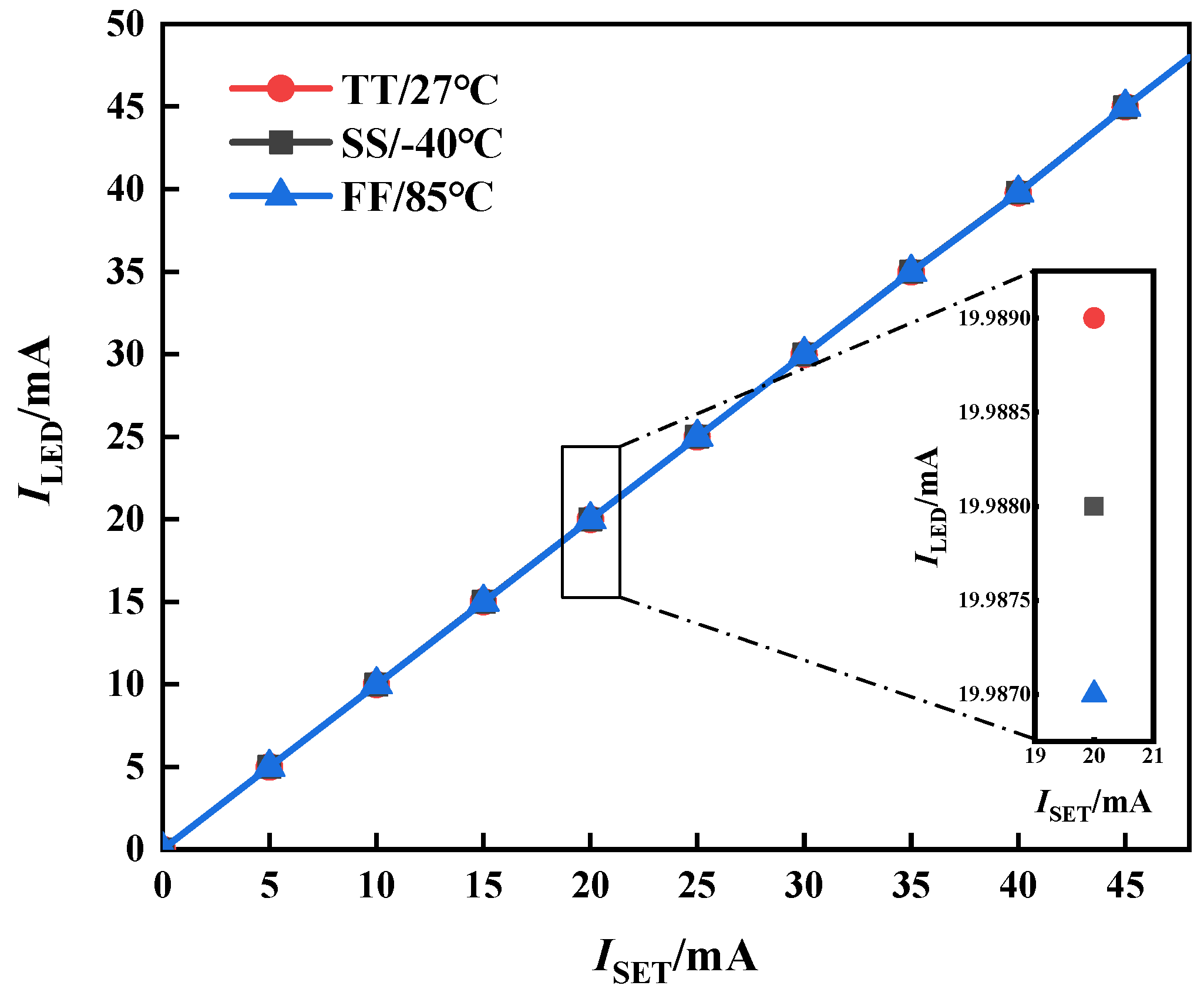
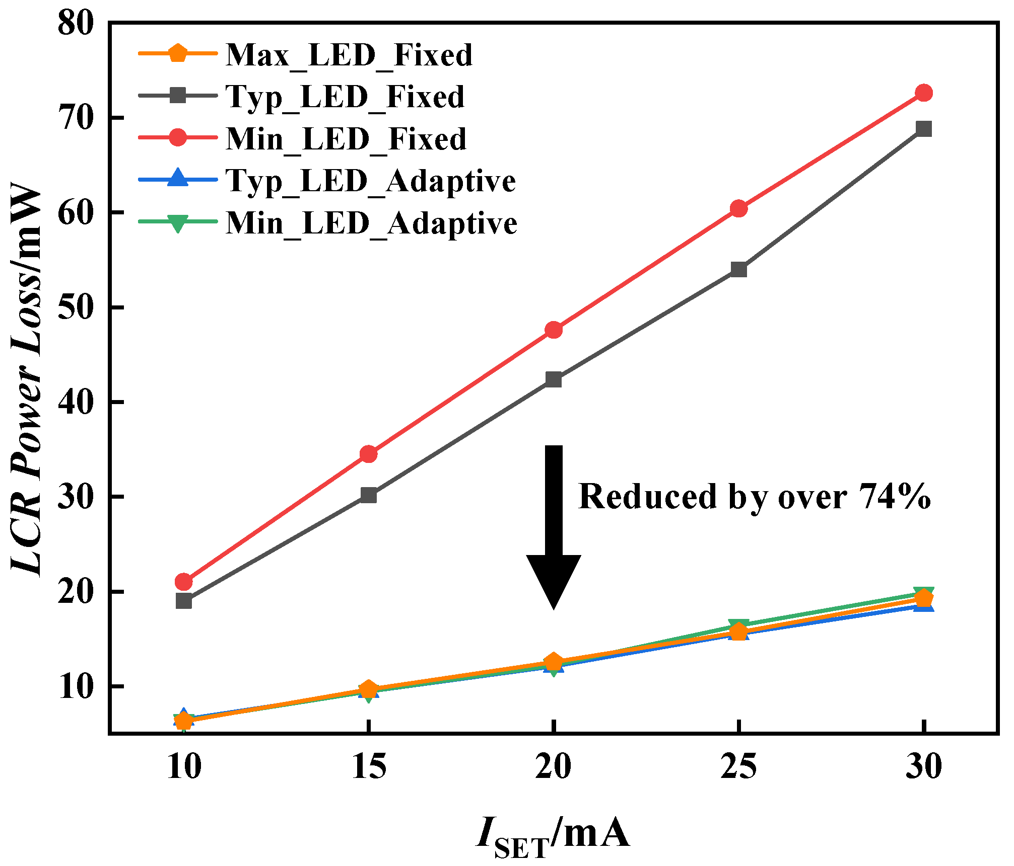
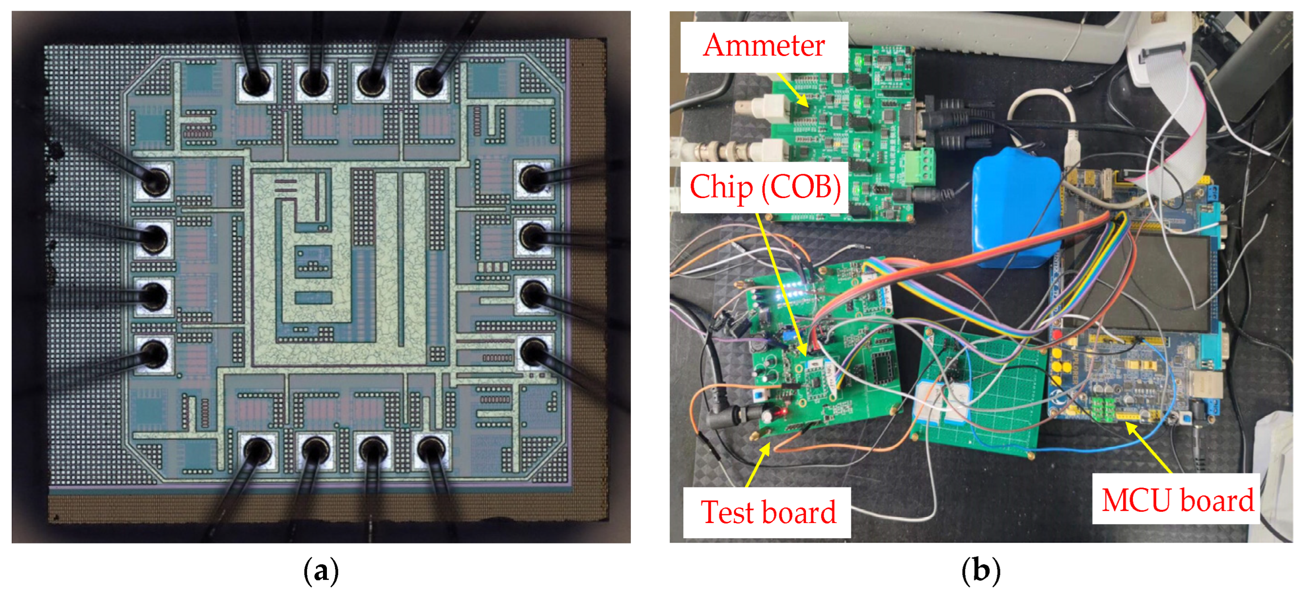
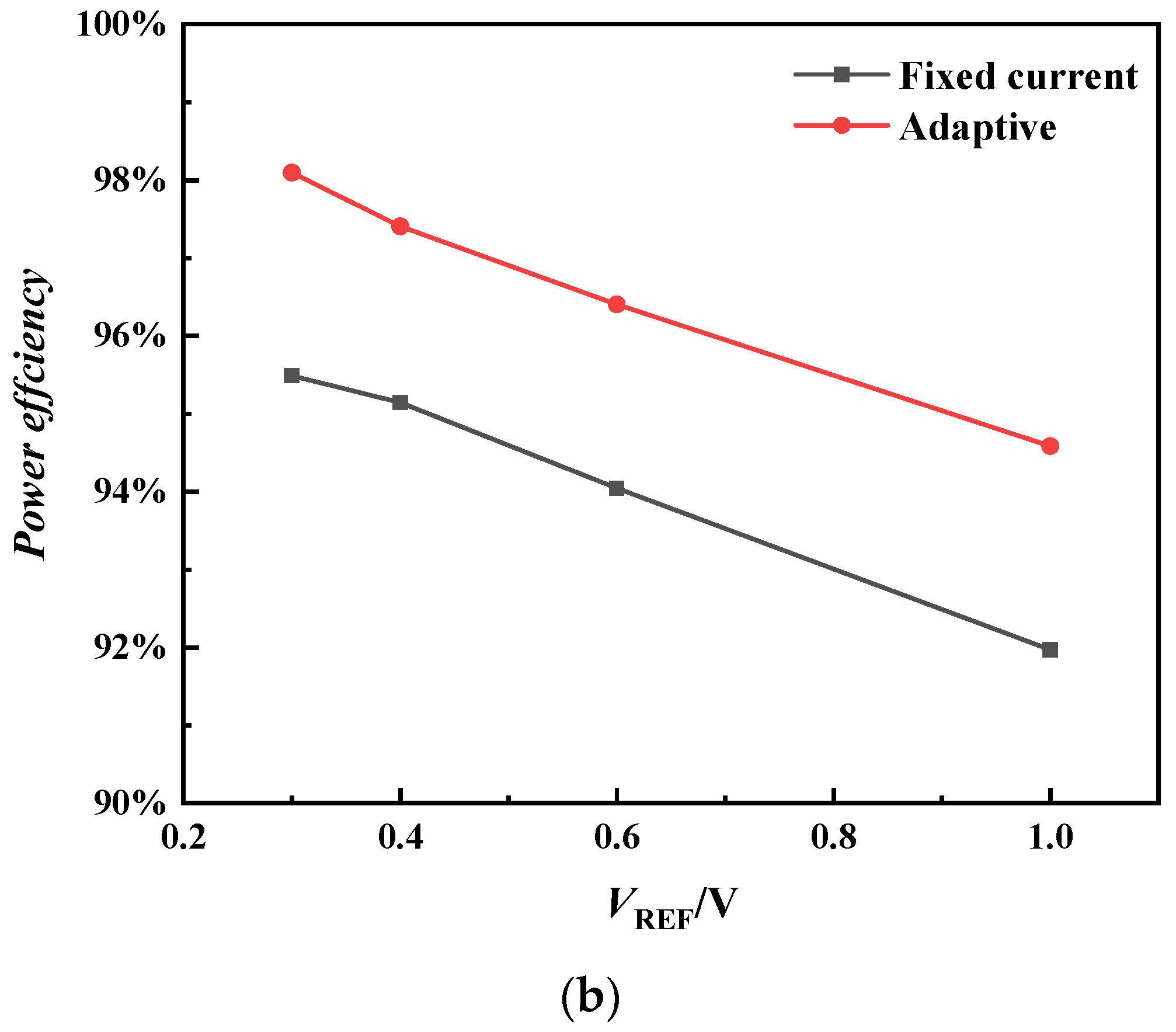
3.3. Measurement Results

Figure 10 displays a microphotograph of the fabricated chip with bonding wires, along with the chip test setup. The chip is housed in a chip-on-board (COB) package and mounted on the test board. The reference current IREF is supplied by the test board. An STM32F407 MCU (from ST Microelectronics) development board serves as the brightness controller, and the integrated DAC in the MCU is used to generate VC. A multi-channel ammeter is connected in series between each LED chain and the drain of the high-voltage MOS transistor to measure the average current of the LED channels. This ammeter supports real-time data recording via a serial port. Voltage waveforms at circuit nodes are captured using a digital oscilloscope, specifically the RTB2004 from Rohde & Schwarz. For simplicity in testing, only two LED channels are implemented, each comprising 6 LEDs. It is noteworthy that the LEDs are intentionally selected to create a difference of approximately 500 mV in the forward voltage across the LED chain between the two channels. Channel 2 has the smaller forward voltage. This deliberate difference enhances the demonstration of the circuit’s effectiveness.
The indoor temperature was maintained at around 27 °C. Figure 11 illustrates the measured voltage waveforms of VPWM and Vloss for channel 2 after the initial adaptive control process. The channel current setting Iset is 20 mA. The four figures correspond to the case when VREF is set to 1 V, 0.6 V, 0.4 V, and 0.3 V, respectively. The duty cycle of VPWM in each case is recorded as 68.57%, 68.86%, 68.43%, and 68.53%, respectively. When VPWM is high, the channel is turned on, and Vloss in each case is measured at 1.06 V, 0.69 V, 0.49 V, and 0.36 V, respectively. When VPWM transitions low, the channel is closed, and the increase in Vloss attributes mainly to the influence of leakage current effects. It can be inferred from the figures that despite VREF decreasing from 1 V to 0.3 V, which may cause the current mirror transistors in the LCR to enter the linear region, the accuracy of the output current can still be maintained, and the duty cycle of VPWM remains consistent across these settings.
Figure 12 shows the difference in Vloss and power efficiency of channel 2 under both the fixed peak current control method and the adaptive control method. From Figure 12a, it is very obvious that there is an excessive voltage of about 500 mV in channel 2. With the adaptive control method, this excessive voltage is effectively mitigated through adjustments in ILED, resulting in a substantial improvement in power efficiency. Specifically, when VREF is set to 300 mV, the power efficiency can reach 98.1% at an ILED of 20 mA. In principle, it is possible to further improve the power efficiency by reducing VREF even further, with the upper limit constrained by VCOM, which is up to the power supply.
Table 1 compares various parameters and performance metrics between the proposed adaptive driver and other existing references. The proposed design demonstrates advantages such as a wide output current range and high power efficiency. In fact, Table 1 only reveals the efficiency of a single channel. However, more importantly, the proposed adaptive method aims to improve the efficiency of each channel in a multi-channel LED driver. It effectively compensates for excessive voltage on the LCR through adaptive control with moderate implementation complexity.

4. Summary

In this paper, an adaptive high-efficiency LED backlight driver is designed to address the issue of excessive power loss caused by variations in the forward voltage of LEDs. By adjusting the peak current, the consistency in the forward voltage of the LED chain within each channel is achieved. This minimizes the voltage on the LCR in each channel, thereby optimizing the excessive power loss in each channel and the total power efficiency. Furthermore, adjusting the duty cycle ensures brightness consistency across each channel. Based on the 0.18 μm 1P4M CMOS process, an LCR circuit suitable for adaptive control was designed and fabricated. The circuit utilizes a current mirror structure and MOS transistors operating in the linear region to ensure current accuracy and power efficiency. The designed LCR circuit supports an output current range of 0–48 mA. To verify the effectiveness of the adaptive control circuit, an experimental two-channel LED backlight driver was constructed using the designed LCR chips. Each channel consists of 6 LEDs, and the forward voltage difference between channels is intentionally expanded to approximately 500 mV. The test results demonstrate that the presented adaptive control circuit eliminates this forward voltage difference and reduces the excessive power loss. When the reference voltage is set to 300 mV, a power efficiency of 98.1% is achieved at 20 mA. In fact, the experimental two-channel driver can be extended to multi-channel implementation. While only an LCR chip is designed and fabricated in this study, the MP transistors and the brightness controller can both be integrated to realize a monolithic integrated driver chip using BCD processes.

Author Contributions

Conceptualization, W.Z. and Q.Z.; methodology, X.X., Q.Z., C.J. and Z.Z.; software, X.X.; validation, X.X., Q.Z., C.J. and Z.Z.; formal analysis, X.X.; investigation, X.X., Q.Z., C.J. and Z.Z.; resources, X.X. and Q.Z.; data curation, X.X. and Q.Z.; writing—original draft preparation, X.X. and Q.Z.; writing—review and editing, W.Z. and X.X.; supervision, W.Z. and J.T.; project administration, W.Z. and J.T.; funding acquisition, W.Z. All authors have read and agreed to the published version of the manuscript.

Funding

This research was funded by Hunan Provincial Department of Education Scientific Research Project (23A0260) and Changsha University of Science and Technology Graduate Practice Innovation Project (CLSJCX24079).

Data Availability Statement

The data presented in this study are available on request from the corresponding author.

Conflicts of Interest

The authors declare no conflicts of interest.

References

  1. Tsao, J.Y. Solid-state lighting: Lamps, chips, and materials for tomorrow. IEEE Circuits Devices Mag. 2004, 20, 28–37. [Google Scholar] [CrossRef]
  2. Yadlapalli, R.T.; Narasipuram, R.P.; Kotapati, A. An overview of energy efficient solid state LED driver topologies. Int. J. Energy Res. 2020, 44, 612–630. [Google Scholar] [CrossRef]
  3. Morrow, R.C. LED lighting in horticulture. HortScience 2008, 43, 1947–1950. [Google Scholar] [CrossRef]
  4. Cho, J.; Park, J.H.; Kim, J.K.; Schubert, E.F. White light-emitting diodes: History, progress, and future. Laser Photonics Rev. 2017, 11, 1600147. [Google Scholar] [CrossRef]
  5. Surkanti, P.R.; Mehrotra, D.; Furth, P.M. Multi-channel LED driver with accurate current matching for portable applications. In Proceedings of the 2019 IEEE 62nd International Midwest Symposium on Circuits and Systems (MWSCAS), Dallas, TX, USA, 4–7 August 2019; pp. 941–944. [Google Scholar]
  6. Pal, N.; Fish, A.; McIntyre, W.; Griesert, N.; Winter, G.; Eichhorn, T.; Pilawa-Podgurski, R.; Hanumolu, P.K. A 91% efficient 30 V hybrid boost-SC converter based backlight LED driver in 180 nm CMOS. In Proceedings of the 2020 IEEE Custom Integrated Circuits Conference (CICC), Boston, MA, USA, 22–25 March 2020; pp. 1–4. [Google Scholar]
  7. Pressman, A. Switching Power Supply Design; McGraw-Hill, Inc.: New York, NY, USA, 1997. [Google Scholar]
  8. Wang, Y.; Alonso, J.M.; Ruan, X. A review of LED drivers and related technologies. IEEE Trans. Ind. Electron. 2017, 64, 5754–5765. [Google Scholar] [CrossRef]
  9. Gupta, N.; Verma, D. A review and analysis of topologies of light emitting diode (LED) drivers. In Proceedings of the 2021 IEEE 2nd International Conference on Electrical Power and Energy Systems (ICEPES), Bhopal, India, 10–11 December 2021; pp. 1–6. [Google Scholar]
  10. Oh, T.-J.; Cho, A.; Ki, S.-L.; Hwang, I.-C. A low-power and low-cost digitally-controlled boost LED driver IC for backlights. In Proceedings of the 2012 IEEE Asian Solid State Circuits Conference (A-SSCC), Kobe, Japan, 12–14 November 2012; pp. 237–240. [Google Scholar]
  11. Lee, S.-W.; Choe, H.-J.; Yun, J.-J. Performance improvement of a boost LED driver with high voltage gain for edge-lit LED backlights. IEEE Trans. Circuits Syst. II Express Briefs 2017, 65, 481–485. [Google Scholar] [CrossRef]
  12. Chen, H.; Zhang, Y.; Ma, D. A SIMO parallel-string driver IC for dimmable LED backlighting with local bus voltage optimization and single time-shared regulation loop. IEEE Trans. Power Electron. 2011, 27, 452–462. [Google Scholar] [CrossRef]
  13. Kim, H.-C.; Yoon, C.S.; Jeong, D.-K.; Kim, J. A single-inductor, multiple-channel current-balancing LED driver for display backlight applications. IEEE Trans. Ind. Appl. 2014, 50, 4077–4081. [Google Scholar] [CrossRef]
  14. Chen, J.-H.; Wang, S.-C.; Liu, Y.-H.; Cheng, Y.-S.; Yang, Z.-Z. RGB LED backlight driving system with dynamic voltage regulation capability. In Proceedings of the 2013 IEEE 10th International Conference on Power Electronics and Drive Systems (PEDS), Kitakyushu, Japan, 22–25 April 2013; pp. 349–353. [Google Scholar]
  15. Liu, P.-J.; Hong, Z.-Y.; Hung, C.-C. A single-stage low-power AC–DC RGB-LED driver with switching capacitor control scheme. IEEE Trans. Ind. Electron. 2020, 68, 3103–3112. [Google Scholar] [CrossRef]
  16. Kim, J.-S.; Lee, Y.-K.; Lee, J.-S.; Shin, Y.-K.; Tark, J.-H.; Ryu, K.-C.; Yang, B.-D. A fast-switching current-pulse driver for LED backlight. In Proceedings of the 2009 IEEE International Symposium on Circuits and Systems, Taipei, Taiwan, 24–27 May 2009; pp. 1775–1778. [Google Scholar]
  17. Hong, S.-I.; Han, J.-W.; Kim, D.-H.; Kwon, O.-K. A double-loop control LED backlight driver IC for medium-sized LCDs. In Proceedings of the 2010 IEEE International Solid-State Circuits Conference-(ISSCC), San Francisco, CA, USA, 7–11 February 2010; pp. 116–117. [Google Scholar]
  18. Huang, Y.-C.; Chen, H.-W. A novel fast-switching current-pulse driver for LED backlight applications. In Proceedings of the 2016 IEEE International Conference on Consumer Electronics-Taiwan (ICCE-TW), Nantou, Taiwan, 27–29 May 2016; pp. 1–2. [Google Scholar]
  19. Ahn, H.-A.; Hong, S.-K.; Kwon, O.-K. A fast switching current regulator using slewing time reduction method for high dimming ratio of LED backlight drivers. IEEE Trans. Circuits Syst. II Express Briefs 2016, 63, 1014–1018. [Google Scholar] [CrossRef]
  20. Han, H.; Zhang, F.; Liu, M. PWM dimming method for capacitor-clamped current-sharing circuit in LED backlight system. IEEE J. Emerg. Sel. Top. Power Electron. 2018, 6, 1190–1197. [Google Scholar] [CrossRef]
  21. Hong, S.-I.; Nam, K.-S.; Jung, Y.-H.; Ahn, H.-A.; In, H.-J.; Kwon, O.-K. Highly power-efficient and reliable light-emitting diode backlight driver IC for the uniform current driving of medium-sized liquid crystal displays. J. Inf. Disp. 2012, 13, 73–82. [Google Scholar] [CrossRef]
  22. Lim, B.-M.; Ko, Y.-H.; Jang, Y.-S.; Kwon, O.-H.; Han, S.-K.; Lee, S.-G. A 200-V 98.16%-efficiency buck LED driver using integrated current control to improve current accuracy for large-scale single-string LED backlighting applications. IEEE Trans. Power Electron. 2015, 31, 6416–6427. [Google Scholar] [CrossRef]
  23. Parthasarathy, M.K.; Ganesan, N. A novel single-inductor eight-channel light-emitting diode driver for low power display backlight applications. Turk. J. Electr. Eng. Comput. Sci. 2018, 26, 2130–2139. [Google Scholar] [CrossRef]
  24. He, J.-P.; Zhang, B.; Gao, X.; Wu, C.-D.; Li, Z.-J.; Zhou, J.-Y. A high accuracy weak voltage LED analog dimming method. IEEE Access 2019, 7, 172362–172373. [Google Scholar] [CrossRef]
  25. Lin, C.-L.; Chen, S.-C.; Deng, M.-Y.; Ho, Y.-H.; Lin, C.-A.; Tsai, C.-L.; Liao, W.-S.; Liu, C.-I.; Wu, C.-E.; Peng, J.-T. AM PWM driving circuit for mini-LED backlight in liquid crystal displays. IEEE J. Electron Devices Soc. 2021, 9, 365–372. [Google Scholar] [CrossRef]
  26. Schubert, E.F. Light-Emitting Diodes (2018); Rensselaer Polytechnic Institute: Tory, NY, USA, 2018. [Google Scholar]
  27. Liu, C.-H.; Hsieh, C.-Y.; Hsieh, Y.-C.; Tai, T.-J.; Chen, K.-H. SAR-controlled adaptive off-time technique without sensing resistor for achieving high efficiency and accuracy LED lighting system. IEEE Trans. Circuits Syst. I Regul. Pap. 2009, 57, 1384–1394. [Google Scholar]
  28. Lohaus, L.; Rossius, A.; Dietrich, S.; Wunderlich, R.; Heinen, S. A dimmable LED driver using resistive DAC feedback control for adaptive voltage regulation. In Proceedings of the 2013 IEEE Energy Conversion Congress and Exposition, Denver, CO, USA, 15–19 September 2013; pp. 3126–3133. [Google Scholar]
  29. Hsieh, C.-Y.; Wei, Y.-S.; Chen, K.-H.; Lin, T.-C. Efficienct LED driver with an adaptive reference tracking technique. In Proceedings of the 2009 16th IEEE International Conference on Electronics, Circuits and Systems-(ICECS 2009), Yasmine Hammamet, Tunisia, 13–16 December 2009; pp. 291–294. [Google Scholar]
  30. Liu, P.-J.; Hsu, S.-R.; Chang, C.-W.; Liao, C.-Y.; Chien, L.-H. Dimmable white LED driver with adaptive voltage feedback control. In Proceedings of the 2015 IEEE 2nd International Future Energy Electronics Conference (IFEEC), Taipei, Taiwan, 1–4 November 2015; pp. 1–4. [Google Scholar]
  31. Jung, Y.H.; Hong, S.K.; Kwon, O.K. A fast transient LED driver with adaptive frequency control according to load variation for large-sized LCD backlights. J. Soc. Inf. Disp. 2017, 25, 712–724. [Google Scholar] [CrossRef]
  32. Hsu, Y.-C.; Lin, J.-Y.; Chen, C.C.-P. Area-saving and high-efficiency RGB LED driver with adaptive driving voltage and energy-saving technique. Energies 2018, 11, 1422. [Google Scholar] [CrossRef]
  33. Yong, W.; Baoxing, D.; Yi, L.; Ting, L.; Yintang, Y. A Multi-channel High Efficiency Boost LED Backlight Driver with High Dimming Ratio. In Proceedings of the 2017 International Conference on Electronic Industry and Automation (EIA 2017), Suzhou, China, 23–25 June 2017; pp. 110–116. [Google Scholar]
  34. Hsieh, Y.-T.; Liu, B.-D.; Wu, J.-F.; Fang, C.-L.; Tsai, H.-H.; Juang, Y.-Z. A high-dimming-ratio LED driver for LCD backlights. IEEE Trans. Power Electron. 2012, 27, 4562–4570. [Google Scholar] [CrossRef]
  35. Chiu, H.-J.; Lo, Y.-K.; Chen, J.-T.; Cheng, S.-J.; Lin, C.-Y.; Mou, S.-C. A high-efficiency dimmable LED driver for low-power lighting applications. IEEE Trans. Ind. Electron. 2009, 57, 735–743. [Google Scholar] [CrossRef]
  36. Hu, Y.; Jiang, L.; Wen, W.; Yan, W.; Ding, R. A new adaptive drive voltage approach for LED driver. In Proceedings of the 2019 IEEE Applied Power Electronics Conference and Exposition (APEC), Anaheim, CA, USA, 17–21 March 2019; pp. 721–726. [Google Scholar]
  37. Wu, C.-H.; Chen, C.-L. High-efficiency current-regulated charge pump for a white LED driver. IEEE Trans. Circuits Syst. II Express Briefs 2009, 56, 763–767. [Google Scholar]
  38. Mu, H.; Geng, L.; Liu, J. A high precision constant current source applied in LED driver. In Proceedings of the 2011 Symposium on Photonics and Optoelectronics (SOPO), Wuhan, China, 16–18 May 2011; pp. 1–4. [Google Scholar]
  39. Sansen, W.M. Analog Design Essentials; Springer Science & Business Media: Berlin, Germany, 2007; Volume 859. [Google Scholar]
  40. Hogervorst, R.; Tero, J.P.; Eschauzier, R.G.; Huijsing, J.H. A compact power-efficient 3 V CMOS rail-to-rail input/output operational amplifier for VLSI cell libraries. IEEE J. Solid-State Circuits 1994, 29, 1505–1513. [Google Scholar] [CrossRef]
  41. Surkanti, P.R.; Mehrotra, D.; Gangineni, M.; Furth, P.M. Multi-string LED driver with accurate current matching and dynamic cancellation of forward voltage mismatch. In Proceedings of the 2017 IEEE 60th International Midwest Symposium on Circuits and Systems (MWSCAS), Boston, MA, USA, 6–9 August 2017; pp. 229–232. [Google Scholar]
  42. Shahroury, F.R.; Ahmad, H.H.; Abuishmais, I. Design Aspects of a Single-Output Multi-String WLED Driver Using 40 nm CMOS Technology. J. Low Power Electron. Appl. 2022, 12, 5. [Google Scholar] [CrossRef]
  43. Abuishmais, I.; Shahroury, F.R.; Ahmad, H. A Design Methodology of High-Efficiency Dimmable Current Sink for Current-Regulated Drivers. Electronics 2022, 11, 2566. [Google Scholar] [CrossRef]
Figure 1. Structure of the proposed adaptive high-efficiency LED backlight driver.
Electronics 13 03057 g001
Figure 2. Flowchart of the adaptive control process in the initialization phase.
Electronics 13 03057 g002
Figure 3. Typical linear current regulator circuits. (a) Source regulation structure; (b) Mirror current structure.
Electronics 13 03057 g003
Figure 4. LCR circuit for adaptive control.
Electronics 13 03057 g004
Figure 5. Layout of LCR, designed in a 0.18 μm CMOS process and the core area is 325 × 310 μm2. The key transistor sizes are also summarized.
Electronics 13 03057 g005
Figure 6. Output current of LCR versus current setting under various working condition.
Electronics 13 03057 g006
Figure 7. Voltage waveforms under the adaptive control process.
Electronics 13 03057 g007
Figure 8. Current waveforms of each channel under the adaptive control process.
Electronics 13 03057 g008
Figure 9. Power losses of LCR with the fixed peak current method and the proposed adaptive control method.
Electronics 13 03057 g009
Figure 10. (a) Microphotograph of LCR chip; (b) test system.
Electronics 13 03057 g010
Figure 11. Voltage waveforms of VPWM and Vloss under (a) VREF = 0.3 V, (b) VREF = 0.4 V, (c) VREF = 0.6 V, and (d) VREF = 1 V. Iset = 20 mA.
Electronics 13 03057 g011
Figure 12. Comparison between the fixed peak current method and the proposed adaptive control method in regard to (a) Vloss and (b) power efficiency.
Electronics 13 03057 g012aElectronics 13 03057 g012b
Table 1. Performance parameters comparison.
Ref[17][41][42][43]This work
Process0.35 μm BCD0.5 μm CMOS40 nm CMOS40 nm CMOS0.18 μm CMOS
Core area (mm2)N/A +N/A +N/A +N/A +0.1
Power supply (V)6–273–4.23.2–4.23.2–4.25
Maximum ILED (mA)3020252548
LED chain config.82666
Vboost (V)26.415.3622.52018.96 *
Vloss (mV)~400~300~675~480360 *
Power Efficiency98.4%94.4%97%97.6%98.1% *
Vboost adjustmentYesYesYesYesYes
Channel-by-channel adjustmentNoNoNoNoYes
* Measured at Iset = 20 mA, δset = 100%. + Not available.
Disclaimer/Publisher’s Note: The statements, opinions and data contained in all publications are solely those of the individual author(s) and contributor(s) and not of MDPI and/or the editor(s). MDPI and/or the editor(s) disclaim responsibility for any injury to people or property resulting from any ideas, methods, instructions or products referred to in the content.

