Article

MmWave Tx-Rx Self-Interference Suppression through a High Impedance Surface Stacked EBG

by
Adewale K. Oladeinde
1,
Ehsan Aryafar
2,* and
Branimir Pejcinovic
1
1
Department of Electrical and Computer Engineering, Portland State University, Portland, OR 97201, USA
2
Department of Computer Science, Portland State University, Portland, OR 97201, USA
*
Author to whom correspondence should be addressed.
Electronics 2024, 13(15), 3067; https://doi.org/10.3390/electronics13153067
Submission received: 13 June 2024 / Revised: 27 July 2024 / Accepted: 30 July 2024 / Published: 2 August 2024
(This article belongs to the Special Issue Antenna Design and Its Applications)

Abstract

:
This paper proposes a full-duplex (FD) antenna design with passive self-interference (SI) suppression for the 28 GHz mmWave band. The reduction in SI is achieved through the design of a novel configuration of stacked Electromagnetic Band Gap structures (EBGs), which create a high impedance path to travelling electromagnetic waves between the transmit and receive antenna elements. The EBG is composed of stacked patches on layers 1 and 2 of a four-layer stack-up configuration. We present the design, optimization, and prototyping of unit antenna elements, stacked EBGs, and integration of stacked EBGs with antenna elements. We also evaluate the design through both HFSS (High Frequency Structure Simulator) and over-the-air measurements in an anechoic chamber. Through extensive evaluations, we show that (i) compared to an architecture that does not use EBGs, the proposed novel stacked EBG design provides an average of 25 dB of additional reduction in SI over 1 GHz of bandwidth, (ii) unit antenna element has over 1 GHz of bandwidth at −10 dB return loss, and (iii) HFSS simulations show close correlation with actual measurement results; however, measured results could still be several dB lower or higher than predicted simulation results. For example, the gap between simulated and measured antenna gains is less than 1 dB for 26–28 GHz and 28.5–30 GHz frequencies, but almost 3 dB for 28–28.5 GHz frequency band.

1. Introduction

The scarcity of spectrum in the conventional sub-6 GHz bands coupled with increasing demand for wireless capacity has pushed the wireless industry to deploy next generation cellular and WiFi devices over mmWave bands. For example, in the United States Verizon holds the majority of the spectrum in the 28 GHz frequency band and leverages channels with wide bandwidths to increase the wireless capacity. However, mobile data traffic continues to grow considerably every year. For example, Ericsson predicts that average mobile data usage per smartphone is set to rise from 21 GB in 2023 to 56 GB in 2029, and total mobile data traffic is estimated to grow by a factor of around 3 between 2023 and 2029 [1]. It is therefore imperative to seek solutions that can further increase the spectral efficiency of mmWave wireless networks.
At the same time, full-duplex (FD) wireless has recently emerged as a new technology that can double the spectral efficiency of next generation wireless networks. A radio with FD functionality can transmit and receive wireless signals at the same time and on the same frequency band. The key challenge to FD is self-interference (SI), in which the transmit (Tx) antenna on the wireless device causes significant interference to its own receive (Rx) antenna. Initial FD radio designs and prototypes were presented in 2010 [2,3,4] and proved the feasibility of building FD radios. Since then, the community has proposed many FD radio designs with different tradeoffs in terms of SI cancellation level, cost, and scalability to MIMO, among others (for a survey, refer to [5]). However, the majority of these designs are specific to traditional sub-6 GHz wireless networks.
Our goal in this paper is to study the potential for FD in mmWave wireless devices. Specifically, we focus on antenna design as an avenue to not only optimize the radiation pattern but also to reduce SI. Specifically, we propose using separate Tx and Rx antenna elements and embedding a High Impedance Surface novel Stacked Electromagnetic Band Gap (HIS-nSEBG) structure in between them to reduce SI. Our key contributions can be summarized as follows:
  • Design: We present the design steps for a unit patch antenna, stacked EBG, and integration of stacked EBGs in between the antennas. We discuss the theoretical modelling of a band gap as an LC circuit and discuss how different components of EBG contribute to the inductance (L) and capacitance (C) behaviors of the LC circuit. We then refine the initial design with extensive HFSS (High Frequency Structure Simulator) simulations to provide a desirable balance between different objectives, such as return loss, frequency bandwidth, SI reduction, and antenna gain.
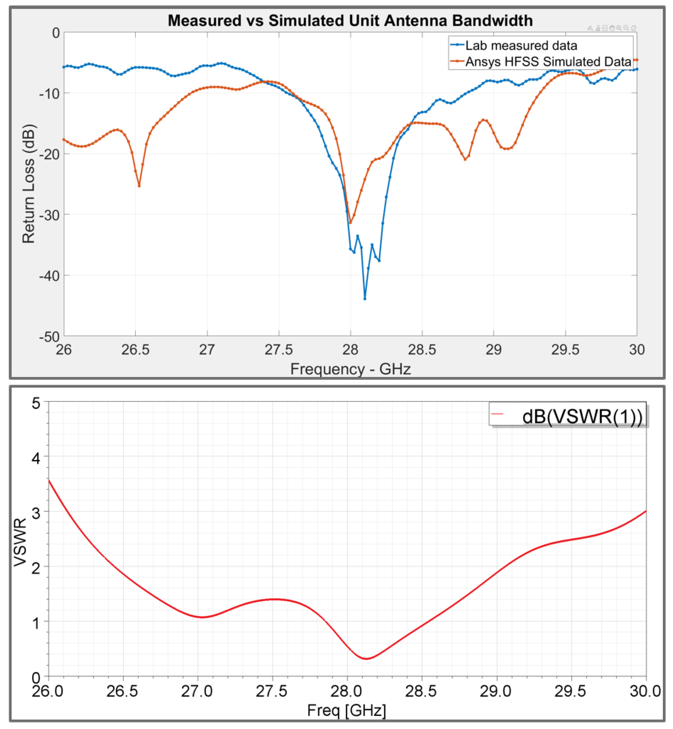
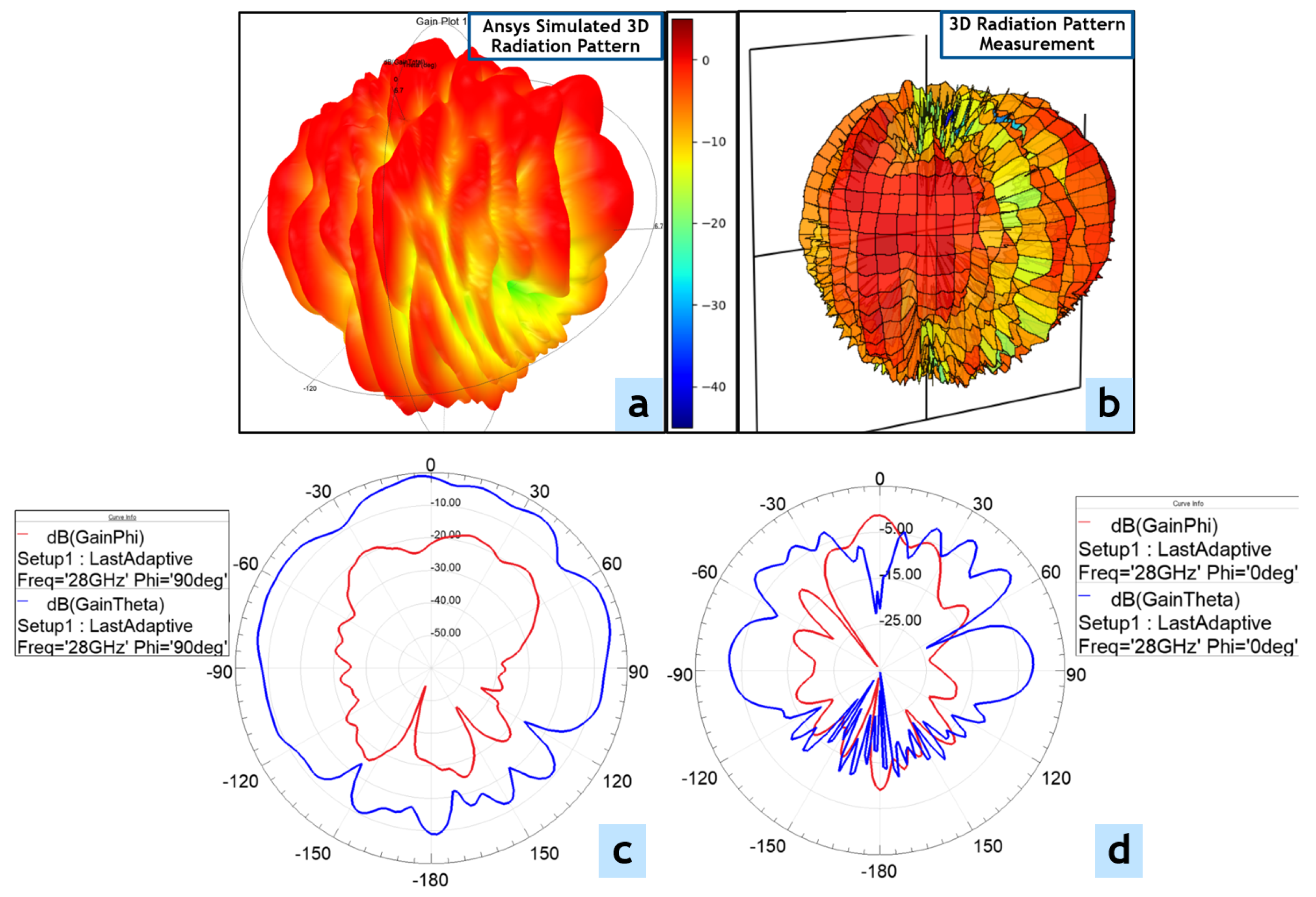
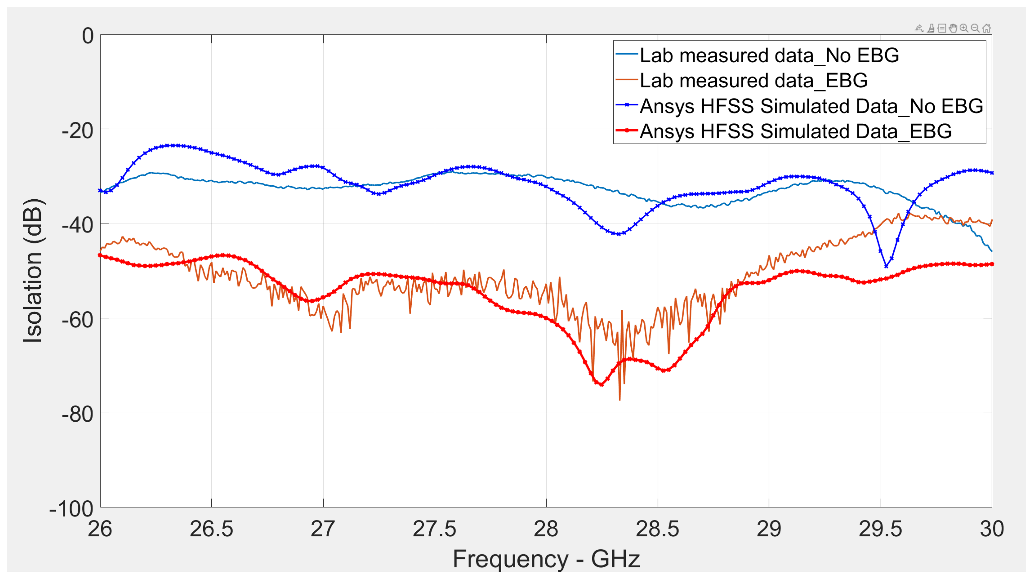
  • Evaluation: We conduct extensive evaluations of our designs through both HFSS simulations and measurements of a prototype. Specifically, we conduct extensive over-the-air measurements of our antennas both inside and outside an anechoic chamber. Our results showed close correlation between simulations and real-world measurements with small deviations resulting from the manufacturing and measurement processes, e.g., we see an average of 2 dB difference in SI reduction prediction between simulation and measurement. However, the gaps can sometimes be large (e.g., more than 10 dB in return loss prediction) at lower and higher frequencies in the case of frequency bandwidth (return loss) plots. Further we show that the proposed design compared to not using EBGs provides more than 25 dB of additional reduction in SI over a 1 GHz of bandwidth.
The rest of this paper is organized as follows. We describe the related work and background on FD wireless and EBGs in Section 2. Next, we design a unit element patch antenna and characterize its return loss, antenna gain, and frequency bandwidth through Ansys HFSS [6] simulations and measurements in an anechoic chamber in Section 3. We discuss the design of our HIS-nSEBG and how to integrate them between Tx and Rx patch antennas in Section 4 and Section 5, respectively. We characterize the overall antenna performance, including port-to-port isolation (i.e., SI reduction) in Section 6. Finally, we conclude the paper in Section 7.

2. Related Work

In this section, we provide a brief background to FD wireless radio design and EBGs. We also discuss some of the related work in these areas.

2.1. Full-Duplex Radio Design

Consider a small handheld device or a femto cell with 20 dBm transmission power and noise floor around −93 dBm. To enable FD, one would need to cancel 20 + 93 = 113 dB of SI. This large amount of SI can be removed over multiple stages, namely antenna, analog, and digital cancellation. Figure 1 depicts how different SI cancellation blocks can be incorporated in the design of a typical radio to enable FD.
Antenna cancellation is primarily a passive SI cancellation technique that arranges Tx and Rx antennas and/or uses RF elements such as reflectors, absorbers, frequency selective surface structures, or EBGs to reduce SI (The proposed antenna system in this paper as well as the majority of the related work in antenna cancellation would not by themselves impact the power consumption, as they are only passive techniques. However, FD operation would activate both transmit and receive paths (RF chains) of the radio, which entail active elements and draw power. This increase in power consumption, however, comes at the benefit of a higher system capacity (i.e., bi-directional communication)). A common strategy here is to use separate Tx and Rx antennas to benefit from path loss and then use other methods (e.g., extra antennas) for additive SI gains [3,4,7,8,9,10,11,12]. Similarly, the work in [13] uses a defected ground structure (DGS) in the ground plane and an MT-30 absorber on top of the array to achieve a high isolation. In another work [14], a 16 dB isolation was achieved by developing a diamond shaped decoupling network with two inverted-F antennas. In [15], a decoupling structure has been introduced that employs a parasitic element to emit orthogonal polarized fields to nullify the coupling field around an Rx antenna in a collinear FD dipole array, bringing the total isolation to 50 dB. Furthermore, other literature has explored the use of cross-polarization between transmitting and receiving antenna elements. For example, refs. [16,17] have demonstrated that up to 10 dB of isolation can be achieved with cross polarization. Cross polarization can be combined with other antenna cancellation techniques for additive/additional SI reduction gains.
Analog cancellation is an active cancellation technique that requires knowledge of the SI channel to create a copy of the SI signal in the RF domain and cancel it before the signal is digitized [2,18,19]. Digital Cancellation is another active cancellation technique that requires knowledge of the SI channel to recreate digital samples of the transmitted signal in the digital domain and subtract them from received samples to remove remaining SI that cannot be removed through antenna and analog cancellation [2].
The majority of the related work in FD radio design is specific to sub-6 GHz radios, with mmWave FD only recently gaining popularity. For example, in [20], the authors develop mmWave circulators to reduce SI. In mmWave systems antenna sizes are very small relative to their wavelength. Thus, one can use separate Tx and Rx antennas for even higher reduction in SI due to over-the-air path loss. Other work has built a custom IC that achieves high bandwidth analog cancellation at mmWave frequencies [21]. Our work can be integrated with this design for further reduction in SI.

2.2. Electromagnetic Band Gaps

An electromagnetic band gap (EBG) is a phenomenon in which certain materials or structures exhibit a range of frequencies within which electromagnetic waves are prohibited from propagating. Essentially, it creates a band of frequencies where electromagnetic waves, such as radio waves or microwaves, cannot travel through the material or structure. EBGs are typically engineered using periodic structures, such as arrays of conducting elements or dielectric materials arranged in a specific pattern. These structures interfere with the propagation of electromagnetic waves by creating constructive and destructive interference patterns, resulting in band gaps where waves are forbidden to propagate. EBGs have gained widespreadd use in a a variety of applications such as antenna design, microstrip circuits, metamaterials, and photonic crystals, among others [22,23,24]. A useful list of EBG applications for antenna engineering is given in [25].
EBGs have been used in the related work to reduce mutual coupling. For example, in [23] EBGs have been used to provide an isolation of 14 dB in 28 GHz band as compared to non-EBG design. Further, additional reduction in coupling is achieved by placing hair-pin DGS on the ground plane, resulting in maximum isolation of 48 dB [24]. Our design provides a higher level of peak isolation with a more compact design (smaller periodicity/size). In other work [26,27], EBGs have been used to simultaneously miniaturize the antennas and reduce the mutual coupling in Sub-6 GHz frequency bands. Similarly, [28] proposed a compact EBG design at 60 GHz and showed that (i) the design has a maximum of 30 dB reduction in mutual coupling with 200 MHz isolation bandwidth, and (ii) the size of the proposed EBG unit cell structure is 78% less than the conventional uniplanar EBG and 72% less than the uniplanar-compact EBG (UC-EBG) operating at same frequency [29]. It is also claimed that the proposed EBG has 12% more size reduction than any other planar EBG structures at microwave frequencies. Our HIS-nEBG design achieves more than 72 dB reduction in mutual coupling with 1 GHz of isolation bandwidth and with the same EBG size. Further, ref. [30] used a combination of EBGs and choke structure to improve the Tx and Rx isolation of X-band large antenna arrays by 30 dB within a 3% bandwidth in the radar operation band. The achieved isolation and its associated bandwidth are due to a combination of using thicker substrate material and choke structures. However, the periodicity and shape of the EBG is large compared to the wavelength, which makes it undesirable for mutual coupling reduction in a compact design. Our proposed HIS-nEBG achieve a compact size through the use of stacked slotted patches, and also achieves a higher mutual coupling isolation. Note that this is the first time a stacked EBG with slotted patch has been designed and implemented for Tx-Rx isolation at 28 GHz band with a periodicity (size) simmilar to that of an EBG in 60 GHz band [28]. In our prior work [31,32], we discussed preliminary EBG-based antenna designs to reduce SI and evaluated their performance through simulations. In this work, we further optimize our antenna and EBG designs to provide more SI isolation and better antenna performance. It is important to note that our prior work [31] uses a combination of a novel VicCross EBG and a defected ground structure on the ground plane to achieve higher antenna-to-antenna isolation. In our current design, a stacked novel type EBG with slotted patch was employed to achieve a much higher peak isolation and bandwidth. Moreover, we prototyped our designs and evaluated their performance through over-the-air measurements in addition to HFSS-based simulations.

3. Unit Antenna Element Design and Characterization

In this section, we discuss the design and performance evaluation of a unit antenna element composed of a rectangular patch. Later in Section 5, we use two copies of this unit antenna element to create separate Tx and Rx antennas on a single wireless device (substrate PCB) and will embed HIS-nEBG structure in between the two antennas elements to reduce SI. The choice to have two separate Tx and Rx antennas is due to the following reasons: (i) antenna separation itself provides more than 30 dB reduction in SI, as we show through lab-measured data in Section 6, and (ii) smaller wavelengths associated with mmWave bands allow us to pack many antennas on the same wireless device, which in turn allows us to use this degree of freedom for SI cancellation.

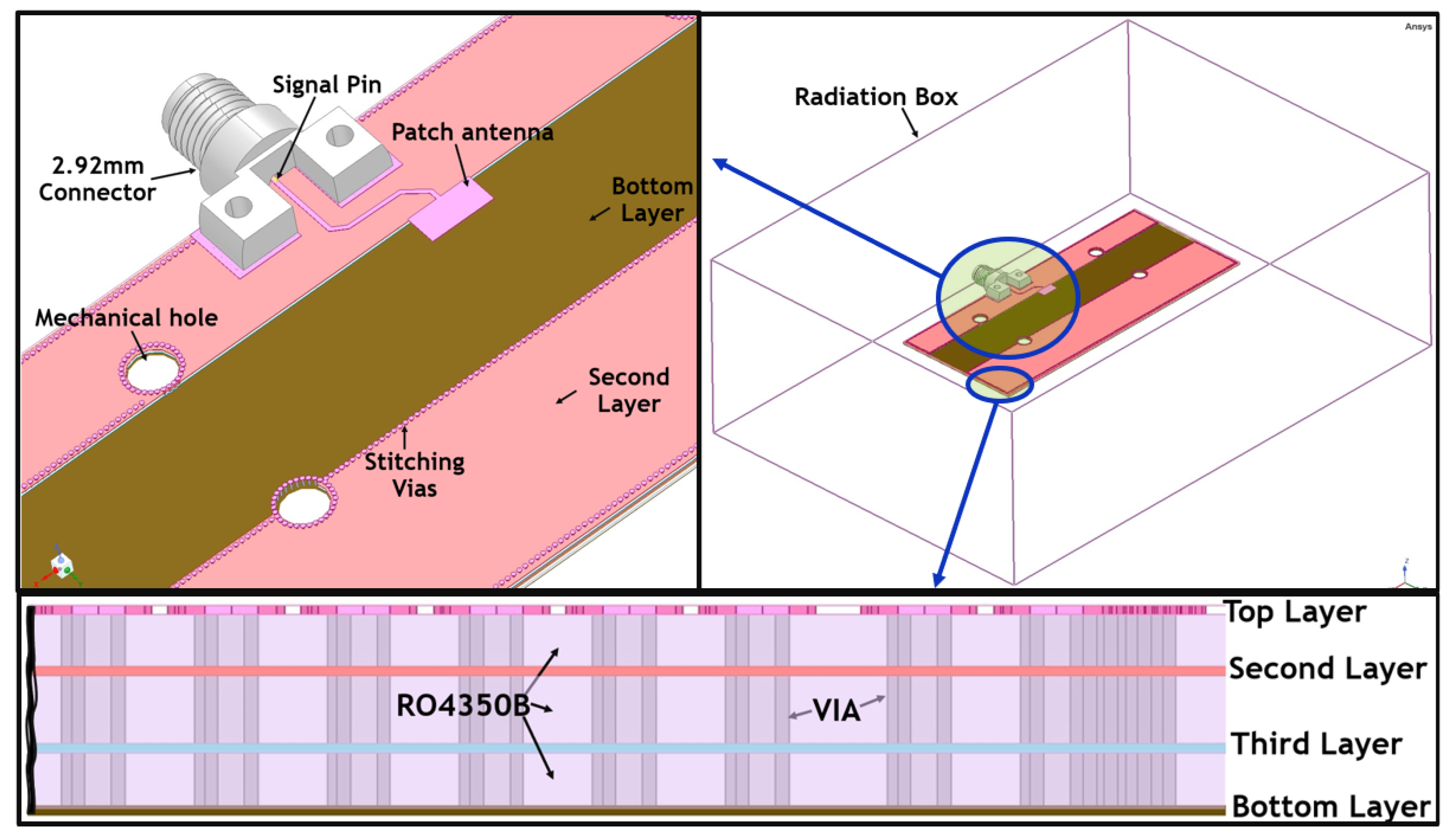
3.1. Design of the Rectangular Patch Antenna

We consider an edge-fed rectangular patch antenna in our design due to its ease of fabrication in mmWave bands, ease of integration into circuits and systems (as well as in our overall FD design), and its simple feed line technique (These advantages come at the cost of lower antenna gains, narrower bandwidth, and excitation of surface waves). Our design is focused on 28 GHz frequency band, which is used for 5G cellular mmWave communication.
Figure 2 (top right) shows the 3D view of the rectangular patch antenna design on a four-layer stack-up structure. The top layer of stack-up is used for a rectangular patch antenna implementation and pad contact for a 2.92 mm RF connector connection, as shown in Figure 2 (top left). The second layer (L2) is used as a ground (GND) reference plane for the patch antenna lead-in trace. A rectangular void structure on L2 is created under the patch antenna for improved antenna efficiency. A similar rectangular void structure is created on the third layer (L3) to further improve the antenna performance. A solid GND layer is defined at the bottom layer as GND reference, which also has mechanical connection for RF connector assembly. Four mechanical non-Plated (NP) holes are added to the PCB design to allow for mechanical support of the Antenna Under Test (AUT) during 3D radiation pattern measurements, as we will discuss later in this section. Rogers RT-Duroid laminate RO4350B (Temperature variations can cause variations in the measured performance metrics. Our selected Rogers material has a low coefficient of thermal expansion and high glass transition temperature to minimize such impacts) and RO4450F pre-preg (Pre-preg is a composite material made from “pre-impregnated” fibers and a partially cured polymer matrix, such as epoxy or phenolic resin, or even thermoplastic mixed with liquid rubbers or resins [33]) materials with a permittivity (Er) of 3.66 and a loss tangent (tand) of 0.0037 are used for the stack-up construction, as depicted in Figure 2 (bottom). The laminate utilizes both 1080 and 1674 glass type weave for controlled impedance and lower resin contents. Inner and outer copper layers are chosen to have 1 oz/ft2 (0.035 mm thickness) with core and pre-preg thicknesses of 0.254 mm and 0.02 mm, respectively, which leads to a stack-up thickness of 0.85 mm, an optimal thickness required for the chosen 2.92 mm RF connector assembly.
The overall dimension of the AUT PCB design, i.e., Length × Width × Height is designed to be 100 mm × 45 mm × 0.85 mm to allow for radiation pattern measurements using a modular millimeter wave anechoic chamber. The modularity of the millimeter wave anechoic chamber is defined by modular cavity sizes to capture far-field radiation energy at millimeter wave frequencies. The RF connector used in the design is a 50 Ω end launch female 2.92 mm connector with a maximum operating frequency of 40 GHz. A 15 mm microstrip transmission line is used to feed the antenna.
In the design of the patch antenna, the standard antenna equations from [31] guided our initial patch antenna length and width dimensions. Ansys HFSS was then used to optimize for the frequency bandwidth and radiation pattern gain.

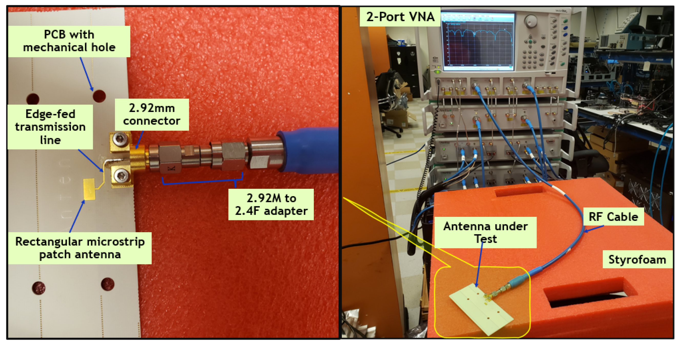
3.2. Unit Antenna Characterization

In this section, we discuss the performance characterization of the fabricated unit antenna element in terms of frequency bandwidth, radiation pattern, and antenna gain. In addition to lab-based measurement data, we also present HFSS [6]-based simulation data to compare and correlate the two data sets.
Figure 3 shows the lab setup for the unit antenna performance characterization using a two port Anritsu [34] Vector Network Analyzer (VNA). A 2.4 mm cable is connected to the antenna under test (AUT) via a 2.92 M (Male) to 2.4 F (Female) adapter. VNA calibration was conducted to the shift reference measurement plane to the RF cable connector end point, including the adapter. The calibration was conducted to allow electrical characteristics of the AUT along with its RF connector to be captured without artifacts or parasites from the measured environment and correctly conduct comparisons with the data obtained through HFSS simulations.
Figure 4 shows the measured and simulated return loss plots for the unit antenna as a function of frequency. At a desirable return loss of −10 dB or lower [23], measured bandwidth for the unit antenna is 1.2 GHz (27.6–28.8 GHz), resulting in a fractional bandwidth of 4.3%, which satisfies the desired bandwidth for Gbps speed mmWave communication at 28 GHz frequency. We also observe that simulation results have high correlation with the measurement results. However, the gaps can sometimes be large (more than 10 dB) at lower and higher frequencies.
In Figure 4, the bottom plot shows the voltage standing wave ratio (VSWR) of the antenna. At the desired 28 GHz frequency, the VSWR value is 0.4:1. This indicates a higher transmitted power, which also translates to a higher efficiency antenna.
We subsequently conducted radiation pattern measurements using an anechoic chamber to determine the measured 3D electric field radiation of the patch antenna. We also conducted simulations for comparison against measurements. Figure 5 shows the Millibox [35] mmWave anechoic chamber that we used for antenna 3D radiation pattern characterization and measurements, with the AUT mounted on a robotic arm on the right side of the chamber. A probe transmitting horn antenna held by another robotic arm on the left side of the chamber is in line-of-sight to the AUT. The distance between the probe antenna and AUT is within the far-field distance of 2 feet, which allows for appropriate characterization of the far-field radiation pattern of the AUT. 3D radiation pattern measurements were taken across the 26 GHz to 30 GHz frequency band. We also rotated the transmitting antenna both vertically (from −90° to 90°) and horizontally (from −90° to 90°) with a step size of 2° for fine-grained radiation pattern measurements (First, the probe antenna was oriented in an H-Polarization state and 3D radiation pattern data were captured with V: −90° to 90° and H: −90° to 90°, with a step size of 2°. Next, the probe antenna was oriented in a V-Polarization state and 3D radiation pattern data were captured with V: −90° to 90° and H: −90° to 90°, with a step size of 2°).
The simulated and measured 3D radiation pattern results for the AUT are shown in Figure 6. We observe a close agreement between the two radiated field plots. Specifically, we observe maximum radiated gains and nulls at similar phi and theta angles in both the measured and simulated plots. The presence of nulls in the measured data, which is also observed in simulation, is due to the destructive interference of near-field coupling between the patch antenna element lead-in trace and the connector. The future planned design of a 1 × 4 patch antenna array for Tx and Rx with an antenna-to-antenna element pitch of λ / 4 with the RF connectors placed side-by-side, necessitated the current placement architecture of the AUT and its connection with the lead-in trace element.
In Figure 6c,d, we have shown simulated H- and E- plane Co and Cross polarization plots. The unit antenna demonstrates a higher Cross polarization compared to Co polarization in the H-plane, as seen in Figure 6c. This is partially due to the proximity of the transmission line to the antenna patch, which may have resulted in destructive interference of TE energy traveling on the transmission line to the linearly polarized transmitted energy from the antenna (We carried out simulations using connector models with wave-ports applied to the RF input of the connector. We modelled the AUT and connector as depicted in Figure 2, which depicted the test set-up used to characterize the AUT in the lab. The use of a connector in the antenna model increases the cross component compared to if we applied the wave-port directly to the trace end of the microstrip transmission line. This can be understood as being due to the amount of impedance discontinuity (mismatch) caused by connector pin impedance and the microstrip trace. The reason we included the connector in our antenna performance results, was to show results that will be representative of what we would encounter in the lab measurement environment (which would use the connector). As a result, our results are representative of the worst-case antenna setup). On the other hand, in the E- plane (Figure 6d), there is a higher Co polarization at the boresight direction. The Cross polarization of the E-plane plot shows a null at the boresight. This suggests that more energy is being transmitted at the antenna boresight direction.
For the main power in the boresight direction of the E-plane cut, we estimated the 3 dB beamwidth to be 20 degrees, which makes the antenna directive in nature, as is required for mmWave communication.
Figure 7 demonstrates the measured and simulated boresight antenna gains as a function of frequency. A close agreement is observed between simulated and measured plots for 26–28 GHz and 28.5–30 GHz frequencies. Within the 500 MHz frequency range of 28–28.5 GHz, we see almost a 3 dB difference in antenna gain (Many factors can contribute to differences between simulated and measured data. For example, (i) Fabrication Inaccuracies: Real-world manufacturing processes may introduce variations in antenna dimensions, shapes, and materials, which are not present in the idealized simulation model. (ii) Measurement Equipment: Calibration, accuracy, and resolution of measurement equipment (e.g., network analyzers, anechoic chambers) can influence results. (iii) Geometry Simplifications: The simulated model may simplify or approximate the physical antenna geometry, leading to discrepancies. (iv) Material Properties: Differences between assumed material properties in simulations (e.g., permittivity, permeability) and actual properties can affect results). The proposed antenna design achieves a measured gain of about 4 dBi within the 28 GHz and 28.5 GHz frequency range of interest. This gain is acceptable for a low-profile patch antenna designed for deployment in various small form factor wireless devices. However, a 5G device manufacturer (e.g., smartphone) may target a slightly higher antenna gain based on their link budget analysis. However, this paper focuses on characterizing the impact of novel EBGs on SI reduction, rather than optimizing individual patch antenna designs. Evaluating our EBG designs with other unit element designs will be part of our future work.

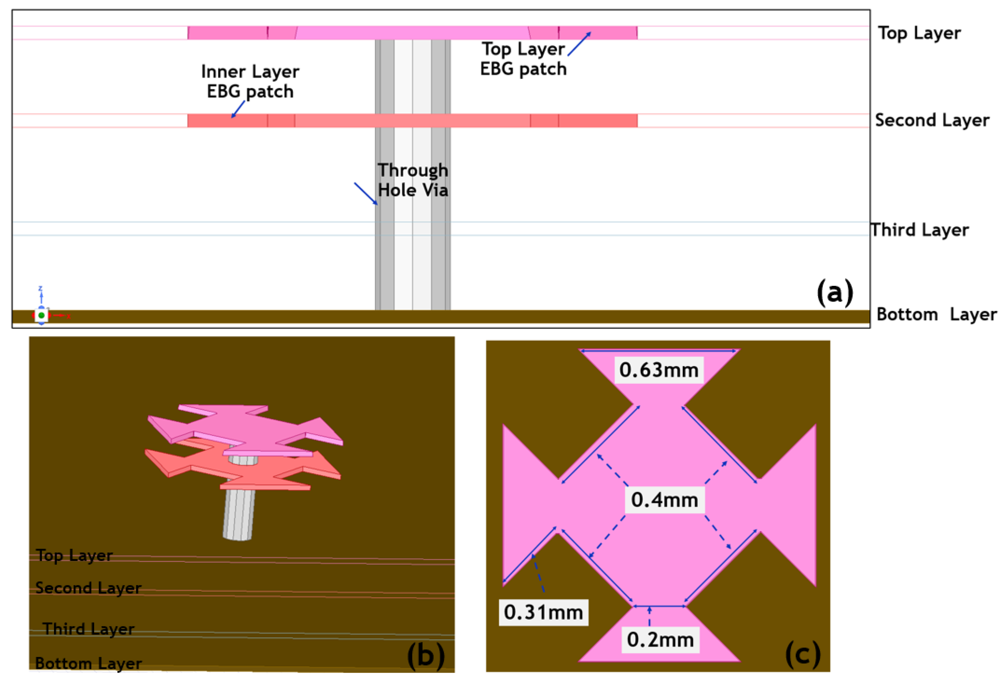
4. High Impedance Surface Novel Stacked Electromagnetic Band Gap (HIS-nSEBG)

In this section, we discuss the details of a novel EBG that is implemented between the Tx and Rx unit antenna elements to reduce SI.
Among the different variations of EBGs, the mushroom-like high impedance surface EBG has become widely used [36], and there have been different variations of mushroom EBGs in the related work that are well suited for antenna design in RF and microwave frequencies. The popularity of EBGs in general is due to their ease of design and manufacturing, especially when it comes to antenna design at sub-6 GHz frequencies. However, integrating EBGs (whether unipolar or mushroom type) as part of antenna design in mmWave bands can be particularly challenging as EBGs need to be compact to properly fit in mmWave transceivers, and the overall design needs to maintain high antenna performance and low overall system complexity.
To illustrate how EBGs can help with antenna performance improvement, consider a microstrip patch antenna on a substrate material, as depicted in Figure 8 (left). Without the use of EBGs, a percentage of the electric field power, relative to the maximum energy transferred to the antenna, radiates from the patch antenna onto free space and the remaining power leaks through the dielectric substrate [37] and copper layers as surface current waves. However, EBGs can be used as part of the antenna design (Figure 8 (right)) to suppress the surface waves and radiate more power towards the main beam to increase the overall antenna efficiency.
In this paper, we develop a novel mushroom-like two-layer stacked EBG structure to reduce port-to-port mutual coupling between the Tx and Rx antennas as a means for passive SI suppression in a mmWave FD radio design. Figure 9 depicts a two-stacked EBG structure in a four-layer (top layer, second layer, third layer, and bottom layer) stack-up design. The stacked type of EBG provides higher SI suppression and higher bandwidth compared to the single stack mushroom EBG [32,36,38].
The surface impedance equation in Equation (1) guided our theoretical optimization in determining the initial size of the through-hole via (which impacts inductance, L) and the stacked EBG patch shapes (which impacts capacitance, C):
Z s u r f a c e = j ω L ( 1 ω 2 L C )
where ω is the angular frequency defined as ω = 2 π f , and f is the desired (resonant) frequency. Further, L and C can be modeled through the following equations:
L = η s ω × tan ( β h )
C = w ϵ 0 ( ϵ r 1 + ϵ r 2 ) π × cosh 1 ( D g )
where η s = μ 0 μ r / ε 0 ε r and β s = ω μ 0 μ r ε 0 ε r defined respectively as the intrinsic wave impedance and propagation constant. ε 0 and μ 0 denote the free space permittivity and permeability, respectively, and ε r and μ r denote the corresponding relative values. D, g and h are EBG pitch (EBG to EBG center), gap (EBG to EBG patch spacing) and EBG height, respectively.
To create a high impedance surface, the denominator in Equation (1) should be set to zero, which results in the following relationship between L, C, and f:
f r e s o n a n c e = 1 2 π × L C
The overall operation of the via and stacked EBG patch is modeled as an LC (resonant) circuit. At frequencies below the resonant frequency, the circuit model becomes inductive and supports TM (transverse magnetic) surface waves, whereas at frequencies above the resonant frequency, the circuit model becomes capacitive and thereby supports TE (transverse electromagnetic) surface waves. At a narrow band around the resonant frequency, surface impedance becomes very high. The novel EBG shape and its stacked formation was designed to further reduce the capacitance effect of the EBG patch (which was needed to increase the isolation bandwidth) and to limit further reduction in patch shape size to accommodate manufacturing limitations. A similar reduction in EBG patch capacitance through creating a novel EBG patch was carried out in a previous paper [31]. In comparison, ref. [31] has a defected ground structure in addition to the VicCross type of EBG with a different stackup and PCB material construction, while our new proposed HIS-nSEBG comprises of defected stacked patch EBGs with a similar orientation for both the top- and inner-layer EBG patches. Both designs have similar periodicity due to similar reduction in EBG patch capacitance that allows us to further improve isolation.
The final dimensions of the stacked EBG are shown in Figure 9 and were achieved after extensive optimization using HFSS to provide a balance between antenna gain, isolation bandwidth, and port-to-port cancellation. We refer to this EBG design as High Impedance Surface novel Stacked EBG (HIS-nSEBG). Note that the patches on the top and second layers of HIS-nSEBG need to be in the same orientation to allow for maximum coupling reduction of surface current waves. This is because with the same patch orientation, the capacitance effect of the stacked patches is maximized, thereby reducing the effective coupling, which increases the isolation bandwidth.

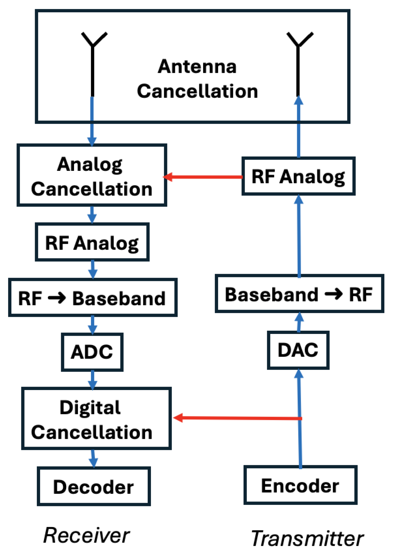
5. EBG Integration with Antennas and Its Operation

In this section, we discuss the integration of the proposed HIS-nSEBG with the Tx and Rx antennas for a complete EBG-based FD antenna system. We also discuss the operational aspects of the electric field coupling between the Tx and Rx antennas resulting from the surface wave radiation through the substrate for both with and without the novel stacked EBG designs.

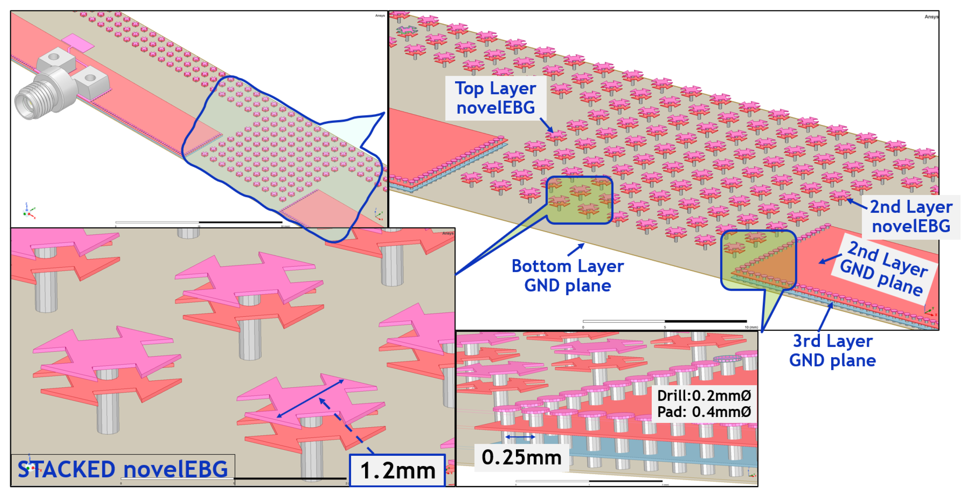
5.1. HIS-nSEBG Integration with Tx and Rx Antennas

We optimized the placement of HIS-nSEBG using Ansys HFSS simulations to achieve high SI suppression between the Tx and Rx antenna elements, while maintaining similar antenna element characteristics in terms of gain and efficiency, as we discussed in Section 3.
Figure 10 shows the placement of HIS-nSEBG structures in between the Tx and Rx antennas. There are 10 columns of HIS-nSEBG structures placed at the center of the design between the Tx and Rx antennas, and the leftmost or rightmost EBG column is 2.5 mm from the solid GND plane. There is a “guard ring” consisting of three rows of HIS-nSEBG along the top and a 3 × 8 column of HIS-nSEBG at the left and right edges. This guard ring is shown in Figure 10 and was optimized to provide optimum antenna gain without degrading the performance of antenna elements, as evaluated in Section 3. Based on simulations, more than 4 mm minimum of spacing is required between HIS-nSEBG and the antenna to maintain gain and antenna efficiency (We conducted numerous HFSS simulations to optimize the design and placement of EBGs such that the reduction in mutual coupling does not come at the cost of antenna gain. Specifically, as we iterated over different simulation parameters, we only considered designs in which the antenna gain of the system with HIS-nSEBG was within 1 dBi of the antenna gain of the design without HIS-nSBG. The reason we chose a 1 dBi tolerance was to accommodate the variations that may arise due to the manufacturing of the design. In the final design that we picked, presented in the paper, and prototyped, the antenna system with HIS-nSEBG has 0.8 dBi higher main-lobe gain and 0.8 dBi lower side lobe level. In other words, there is marginal impact to antenna gain compared to a similar antenna system that does not use EBGs).
Figure 11 shows a close-up view of HIS-nSEBG integration with Tx and Rx antennas. HIS-nSEBG dimensions are shown in the bottom left with top and second layer patches having the same width dimension of 1.2 mm, with similar cutout dimensions of 0.3 mm, 0.4 mm, and 0.28 mm, respectively. Shielding vias, seen on the bottom right, are placed at a distance of 0.25 mm to shield unwanted higher-order electric and magnetic mode resonances, and to attenuate reflected surface current waves from the HIS-nSEBG.
The antenna-to-antenna pitch distance of 47.5 mm (almost 5 λ ) was optimized to allow for a sufficient distance from the center EBGs (to achieve high antenna gains) and to maximize the constructive interference between Tx and Rx antenna surface waves when the radio operates in the FD mode. Further, during the optimization of the HIS-nSEBG using HFSS, it is observed that the novel EBG supports TM surface waves at lower frequencies, TE surface waves at higher frequencies and both TM and TE in between the low and higher frequencies. However, at the resonance frequency, the imaginary part of the surface impedance of the HIS-nSEBG structure becomes large, where both TE and TM surface waves are suppressed, resulting in an electromagnetic surface wave bandgap, thereby isolating the transmit and receive ports (Placement of HIS-nSEBGs in between the antenna elements suppresses surface waves and reduces mutual coupling. By suppressing surface waves, EBG structures reduce undesired electromagnetic interactions that can distort the polarization of the transmitted and received signals. Further, by reducing mutual coupling, they help minimize the introduction of unwanted polarization components. However, the extent of HIS-nSBG impact on polarization purity requires additional performance characterization, which we plan to conduct as part of our future work).

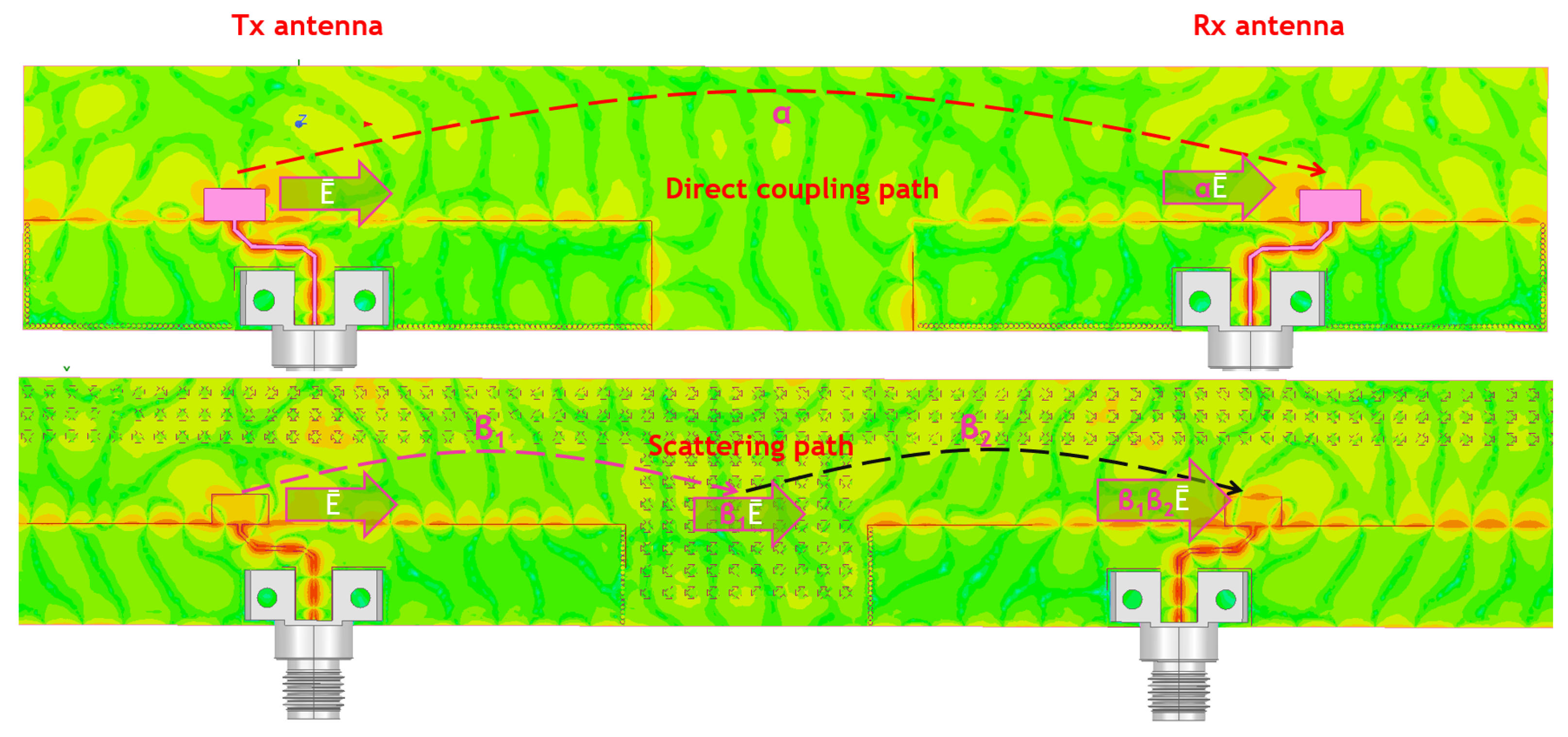
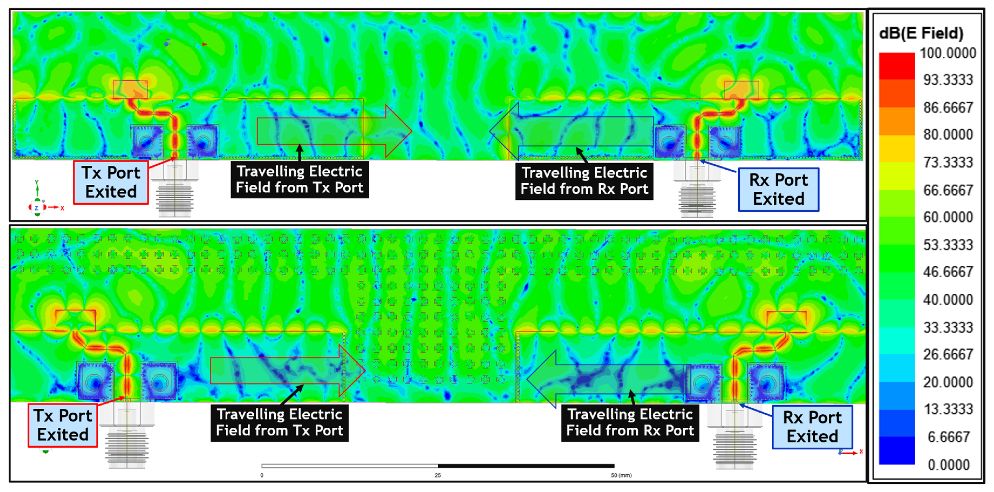
5.2. Operating Mechanism of HIS-nSEBG

The operating mechanism of SI suppression using the HIS-nSEBG described in this work is as seen in Figure 12 based on HFSS simulation plots. The top figure in Figure 12 shows the antenna design without EBGs. Here, the electric field that results from the excitation of the transmitting antenna and movement of charges in substrate and copper layers of PCB is denoted by E . Through the direct coupling path, an electric field α E is induced on the receiving antenna, where α is the coupling coefficient. On the other hand (Figure 12 bottom), by adding HIS-nSEBG structures, a new path condition is generated for the electric field propagation. The coupling coefficient from the transmitting antenna to HIS-nSEBG is given by β 1 , and the coupling coefficient between the HIS-nSEBG and the receiving antenna is given by β 2 . The total induced electric field force at the receiving antenna is given by ( α + β 1 β 2 ) E , and with properly designed passive SI suppression EBG structures in a transceiver system, the electric field in the EBG path produces a reverse coupling of the transmit to receiver antenna coupling:
α E = β 1 β 2 E

6. Measured and Simulated Self-Interference Suppression Results

In this section, we present the SI suppression results of the overall antenna design with HIS-nSEBG embedded in between the antennas. We use both HFSS simulations and over-the-air measurements of a fabricated prototype to derive these results.

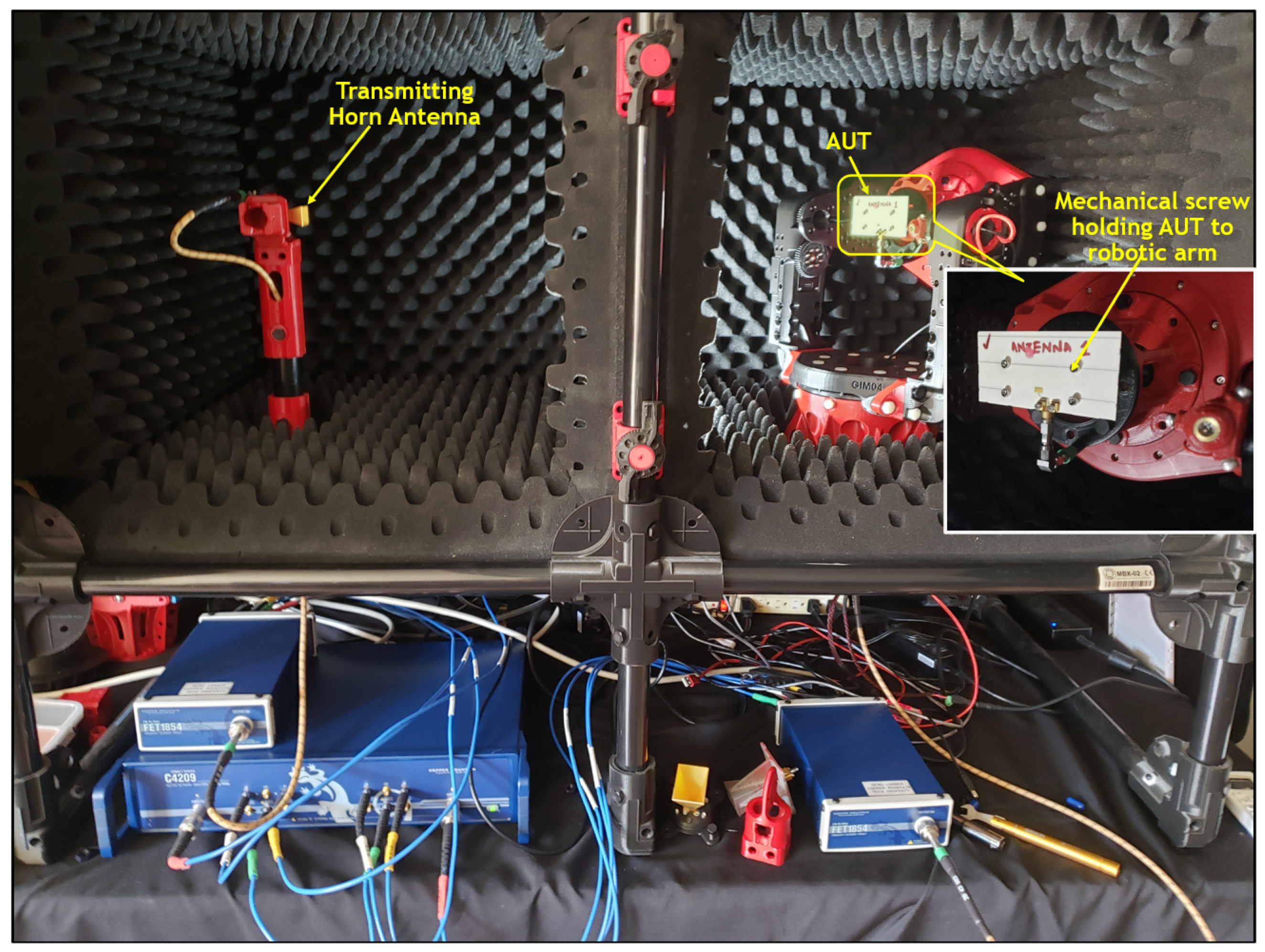
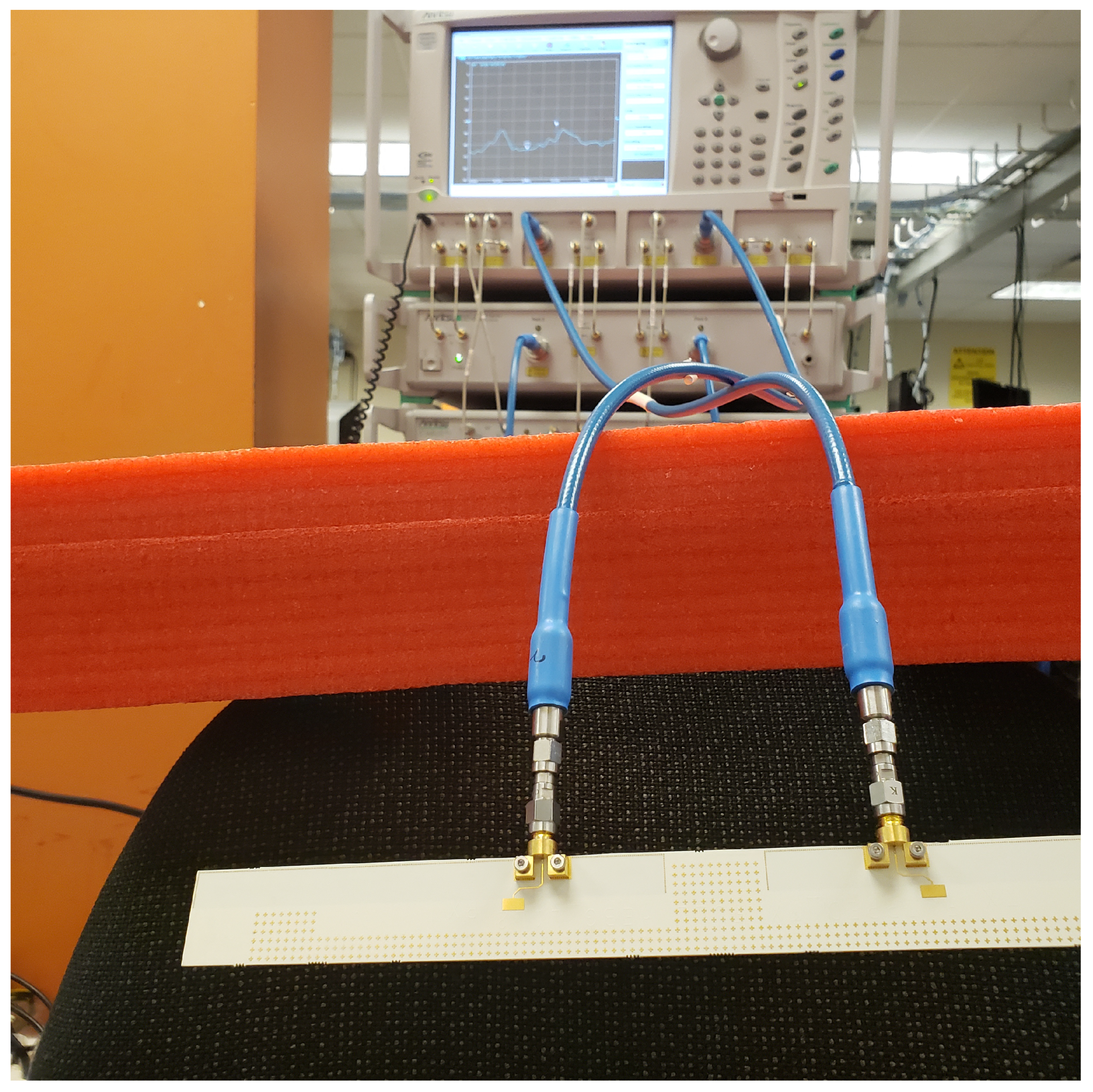
6.1. Measurement Setup

The lab setup for the measurement of the FD antenna system is shown in Figure 13. Anritsu 2-port VNA and RF cable assembly were used to connect to the antenna RF connector ports using a 2.4 mm to 2.92 mm adapter, similar to AUT setup in Section 4.
A 2-port network is a pair of two terminal electrical network and because of its application in transmission networks, one of the ports is called the Input port and the other port, the output port. 2-port network modeling is used in transmission line analysis, where numerous parameters—such as Z, Y, ABCD, H, and T-parameters—define the relationship between dependent and independent quantities. In this work, we used a scattering parameter (S-parameter) model, which is used to model the behavior of linear RF and microwave networks. We have used a 2-port network model of the S-parameter to quantify the reverse transmission coefficient of energy from a transmitter to receiver. The significance of using the transmission coefficient of the S-parameter model is to capture the effect of mutual coupling power or isolation of a transmitting antenna at the receiving antenna. The reverse transmission coefficient is termed as |S12|, where 1 and 2 represent ports 1 and 2 of the 2-port network, respectively.
The Anritsu 2-port VNA setup is used to measure the port-to-port isolation properties, in the form of scattering parameters, of the antenna system with HIS-nSEBG as well as a similar antenna setup that does not use any EBGs. Scattering parameter measurements for the individual antenna elements within the FD system were also conducted to make sure the performance matches the results presented in Section 3.

6.2. Self-Interference Suppression Performance

Figure 14 shows the port-to-port isolation (i.e., SI reduction) results of the two antenna systems as a function of frequency (from 26 GHz to 30 GHz): one with HIS-nSEBG and one with no EBG. For each measured result, we also plot the predicted simulated results from HFSS.
We observe that there is a measured SI reduction of about −30 dB with no EBG, which is due to the over-the-air path loss. The introduction of HIS-nSBG provides an average of 25 dB additional reduction in SI over a 1 GHz bandwidth (27.5–28.5 GHz). We also observe that the measured data (both with and without EBG) track the simulated data with only a few dB of difference, which shows the high fidelity of the simulations in terms of characterizing the reduction in SI.
Figure 15 depicts a snapshot in time of the electromagnetic field distribution between the transmit and receiver antennas, both with (bottom) and without (top) HIS-nSEBG. In the top figure, the TE mode of excited propagating electric field at 28 GHz travelling from Tx to Rx interferes with the propagating wave from Rx to Tx. Further, there is no structure in between the two antennas to create a high impedance path for the propagating fields.
On the other hand, the TE modes of excited propagated electric field with integrated HIS-nSEBG have less interference with one another, which is due to HIS-nSEBG’s creation of the high impedance path.

6.3. Comparison with Other Related Designs

In this section, we provide a summary comparing our work with related work from the literature. Table 1 summarizes isolation and periodicity of different methods according to the EBG type. It is noticeable that our previous work [31], has a periodicity and isolation level that is comparable to this work but with a lower peak isolation. Further, the current design lends itself to easier manufacturing. This allowed us to prototype our design and evaluate its performance with over-the-air measurements in addition to HFSS simulations. Other related works at the same 28 GHz frequency of operation (e.g., [24]) have lower isolation improvement with higher periodicity (and thus more design complexity). Also, when compared to related work at 60 GHz (e.g., [29]), we observe that HIS-nSEBG achieves a higher isolation with comparable periodicity.

7. Conclusions

Full-duplex wireless is an important technology, which promises to double the spectral efficiency of the next generation wireless networks. While the majority of the related work has studied FD wireless in the context of sub-6 GHz wireless radios, this paper studied mmWave FD radio design. Specifically, we showed the design and implementation of a novel EBG architecture that can provide more than a 25 dB reduction in SI. As part of our future work, we plan to extend the design to support a plurality of transmit and receive antennas and study the joint operation of beamforming and antenna design to provide even further reductions in SI.

8. Future Work

Our work in this paper focused on a single Tx and a single Rx antenna, and embedded HIS-nSEBG in between them to reduce SI. As part of our future work, we plan to design an array of Tx and Rx antennas with HIS-nEBG in between them. The plurality of antennas would allow us to characterize the potential for isolation improvement when antenna design is combined with other techniques such as beamforming.
Further, our HIS-nSEBG was designed to suppress linear polarized energy from a unit antenna element with linear polarization. As part of our future work, we plan to design antenna and EBGs that support polarization diversity and evaluate the joint impact of antenna design and polarization diversity to reduce SI in mmWave FD radios.

Author Contributions

Conceptualization, A.K.O., E.A. and B.P.; methodology, A.K.O., E.A. and B.P.; software, A.K.O.; validation, A.K.O.; investigation, A.K.O.; resources, E.A.; data curation, A.K.O.; writing—original draft preparation, A.K.O.; writing—review and editing, A.K.O., E.A. and B.P.; visualization, A.K.O.; supervision, E.A. and B.P.; project administration, E.A. and B.P.; funding acquisition, E.A. All authors have read and agreed to the published version of the manuscript.

Funding

This research was supported in part by an NSF grant (CNS 1942305).

Data Availability Statement

The original contributions presented in the study are included in the article; further inquiries can be directed to the corresponding author.

Acknowledgments

The authors would like to additionally thank the anonymous reviewers for their valuable feedback, which helped improving the quality of this paper.

Conflicts of Interest

The authors declare no conflict of interest.

Abbreviations

The following abbreviations are used in this manuscript:
BSBase Station
FDFull-Duplex
SISelf-Interference
MIMOMultiple Input Multiple Output
TxTransmit
RxReceive
HFSSHigh Frequency Structure Simulator
EBGElectromagnetic Band Gap
HIS-nSEBGHigh Impedance Surface novel Stacked Electromagnetic Band Gap

References

  1. Ericsson: Mobile Network Traffic Update. Available online: https://www.ericsson.com/en/reports-and-papers/mobility-report/dataforecasts/mobile-traffic-forecast (accessed on 1 August 2024).
  2. Duarte, M.; Sabharwal, A. Full-Duplex Wireless Communications Using Off-the-shelf Radios: Feasibility and First Results. In Proceedings of the 2010 Conference Record of the Forty Fourth Asilomar Conference on Signals, Systems and Computers, Pacific Grove, CA, USA, 7–10 November 2010; pp. 1558–1562. [Google Scholar]
  3. Choi, J.I.; Jain, M.; Srinivasan, K.; Levis, P.; Katti, S. Achieving Single Channel, Full Duplex Wireless Communication. In Proceedings of the 16th Annual International Conference on Mobile Computing and Networking and The 11th ACM International Symposium on Mobile Ad Hoc Networking and Computing, Chicago, IL, USA, 20–24 September 2010. [Google Scholar]
  4. Khandani, A.K. Methods for Spatial Multiplexing of Wireless Two-Way Channels. U.S. Patent US7,817,641, 19 October 2010. [Google Scholar]
  5. Smida, B.; Sabharwal, A.; Fodor, G.; Alexandropoulos, G.C.; Suraweera, H.A.; Chae, C.B. Full-Duplex Wireless for 6G: Progress Brings New Opportunities and Challenges. IEEE J. Sel. Areas Commun. 2023, 41, 2729–2750. [Google Scholar] [CrossRef]
  6. Ansys HFSS. Available online: https://www.ansys.com/products/electronics/ansys-hfss (accessed on 1 August 2024).
  7. Yon, H.; Rahman, N.H.A.; Aris, M.A.; Jamaluddin, M.H.; Lin, I.K.C.; Jumaat, H.; Redzwan, F.N.M.; Yamada, Y. Development of C-Shaped Parasitic MIMO Antennas for Mutual Coupling Reduction. Electronics 2021, 10, 2431. [Google Scholar] [CrossRef]
  8. Lin, X.J.; Xie, Z.M.; Zhang, P.S. Integrated Filtering Microstrip Duplex Antenna Array with High Isolation. Int. J. Antennas Propag. 2017, 2017, 4127943. [Google Scholar] [CrossRef]
  9. Everett, E.; Sahai, A.; Sabharwal, A. Passive Self-Interference Suppression for Full-Duplex Infrastructure Nodes. IEEE Trans. Wirel. Commun. 2014, 13, 680–694. [Google Scholar] [CrossRef]
  10. Slingsby, W.T.; McGeehan, J.P. Antenna isolation measurements for on-frequency radio repeaters. In Proceedings of the 1995 Ninth International Conference on Antennas and Propagation, ICAP ’95 (Conf. Publ. No. 407), Eindhoven, The Netherlands, 4–7 April 1995; Volume 1, pp. 239–243. [Google Scholar]
  11. Ramos, A.; Varum, T.; Matos, J.N. A Review on Mutual Coupling Reduction Techniques in mmWaves Structures and Massive MIMO Arrays. IEEE Access 2023, 11, 143143–143166. [Google Scholar] [CrossRef]
  12. Aryafar, E.; Khojastepour, M.A.; Sundaresan, K.; Rangarajan, S.; Chiang, M. MIDU: Enabling MIMO Full Duplex. In Proceedings of the 18th Annual International Conference on Mobile Computing and Networking, Istanbul, Turkey, 22–26 August 2012. [Google Scholar]
  13. Madni, A.; Khan, W.T. Design of a Compact 4-Element GNSS Antenna Array With High Isolation Using a Defected Ground Structure (DGS) and a Microwave Absorber. IEEE Open J. Antennas Propag. 2023, 4, 779–791. [Google Scholar] [CrossRef]
  14. Wu, D.; Cheung, S.W.; Li, Q.L.; Yuk, T.I. Decoupling using diamond-shaped patterned ground resonator for small MIMO antennas. IET Microw. Antenna Propag. 2017, 11, 177–183. [Google Scholar] [CrossRef]
  15. Iwamoto, K.; Heino, M.; Haneda, K.; Morikawa, H. Design of an Antenna Decoupling Structure for an Inband Full-Duplex Collinear Dipole Array. IEEE Trans. Antennas Propag. 2018, 66, 3763–3768. [Google Scholar] [CrossRef]
  16. Nawaz, H.; Tekin, I. Dual-Polarized, Differential Fed Microstrip Patch Antennas with Very High Interport Isolation for Full-Duplex Communication. IEEE Trans. Antennas Propag. 2017, 65, 7355–7360. [Google Scholar] [CrossRef]
  17. Sim, C.Y.D.; Chang, C.C.; Row, J.S. Dual-Feed Dual-Polarized Patch Antenna with Low Cross Polarization and High Isolation. IEEE Trans. Antennas Propag. 2009, 57, 3321–3324. [Google Scholar] [CrossRef]
  18. Kolodziej, K.E.; McMichael, J.G.; Perry, B.T. Multitap RF Canceller for In-Band Full-Duplex Wireless Communications. IEEE Trans. Wirel. Commun. 2016, 15, 4321–4334. [Google Scholar] [CrossRef]
  19. Aryafar, E.; Keshavarz-Haddad, A. PAFD: Phased Array Full-Duplex. In Proceedings of the IEEE INFOCOM 2018—IEEE Conference on Computer Communications, Honolulu, HI, USA, 16–19 April 2018. [Google Scholar]
  20. Reiskarimian, N.; Dastjerdi, M.B.; Zhou, J.; Krishnaswamy, H. Analysis and Design of Commutation-Based Circulator-Receivers for Integrated Full-Duplex Wireless. IEEE J. Solid-State Circuits 2018, 53, 2190–2201. [Google Scholar] [CrossRef]
  21. Singh, V.; Mondal, S.; Gadre, A.; Srivastava, M.; Paramesh, J.; Kumar, S. Millimeter-Wave Full Duplex Radios. In Proceedings of the 26th Annual International Conference on Mobile Computing and Networking, London, UK, 21–25 September 2020; pp. 1–14. [Google Scholar] [CrossRef]
  22. Elsheakh, D.M.N.; Elsadek, H.; Abdallah, E.A. Antenna Designs with Electromagnetic Band Gap Structures. In Metamaterial; InTech: Rijeka, Croatia, 2012; pp. 403–473. [Google Scholar]
  23. Yang, F.; Rahmat-Samii, Y. Microstrip Antennas Integrated with Electromagnetic Band-Gap (EBG) Structures: A Low Mutual coupling Design for Array Applications. IEEE Trans. Antennas Propag. 2003, 54, 2936–2946. [Google Scholar] [CrossRef]
  24. Dey, S.; Dey, S.; Koul, S.K. Isolation Improvement of MIMO Antenna using Novel EBG and Hair-Pin Shaped DGS at 5G Millimeter Wave Band. IEEE Access 2021, 9, 162820–162834. [Google Scholar] [CrossRef]
  25. Yang, F.; Rahmat-Samii, Y. Electromagnetic Band Gap Structures in Antenna Engineering; Cambridge University Press: Cambridge, UK, 2009. [Google Scholar]
  26. Ghosh, S.; Tran, T.N.; Le-Ngoc, T. Dual-Layer EBG-Based Miniaturized Multi-Element Antenna for MIMO Systems. IEEE Trans. Antennas Propag. 2014, 62, 3985–3997. [Google Scholar] [CrossRef]
  27. Farahani, H.S.; Veysi, M.; Kamyab, M.; Tadjalli, A. Mutual Coupling Reduction in Patch Antenna Arrays Using a UC-EBG Superstrate. IEEE Antennas Wirel. Propag. Lett. 2010, 9, 57–59. [Google Scholar] [CrossRef]
  28. Al-Hasan, M.J.; Denidni, T.A.; Sebak, A.R. Millimeter-Wave Compact EBG Structure for Mutual Coupling Reduction Applications. IEEE Trans. Antennas Propag. 2015, 63, 823–828. [Google Scholar] [CrossRef]
  29. Lamminen, A.E.I.; Vimpari, A.R.; Saily, J. UC-EBG on LTCC for 60-GHz Frequency Band Antenna Applications. IEEE Trans. Antennas Propag. 2009, 57, 2904–2912. [Google Scholar] [CrossRef]
  30. Qiu, L.; Zhao, F.; Xiao, K.; Chai, S.L.; Mao, J.J. Transmit–Receive Isolation Improvement of Antenna Arrays by Using EBG Structures. IEEE Antennas Wirel. Propag. Lett. 2012, 11, 93–96. [Google Scholar]
  31. Oladeinde, A.K.; Aryafar, E.; Pejcinovic, B. EBG-Based Self-Interference Cancellation to Enable mmWave Full-Duplex Wireless. In Proceedings of the 2021 IEEE Texas Symposium on Wireless and Microwave Circuits and Systems (WMCS), Waco, TX, USA, 18–20 May 2021. [Google Scholar]
  32. Oladeinde, A.K.; Aryafar, E.; Pejcinovic, B. EBG Placement Optimization in a Via-Fed Stacked Patch Antenna for Full-Duplex Wireless. In Proceedings of the 2022 IEEE-APS Topical Conference on Antennas and Propagation in Wireless Communications (APWC), Cape Town, South Africa, 5–9 September 2022. [Google Scholar]
  33. Pre-Preg. Available online: https://en.wikipedia.org/wiki/Pre-preg (accessed on 1 August 2024).
  34. Anritsu Test and Measurement Equipment. Available online: https://www.anritsu.com/en-us/ (accessed on 1 August 2024).
  35. MilliBox: Benchtop mmWave Antenna Test System. Available online: https://millibox.org/ (accessed on 1 August 2024).
  36. Hassan, M.A.M.; Kishk, A. Bandwidth Study of the Stacked Mushroom EBG Unit Cells. IEEE Trans. Antennas Propag. 2017, 68, 4357–4362. [Google Scholar] [CrossRef]
  37. Yang, F.; Rahmat-Samii, Y. Reflection Phase Characterizations of the EBG Ground Plane for Low Profile Wire Antenna Applications. IEEE Trans. Antennas Propag. 2003, 51, 2691–2703. [Google Scholar] [CrossRef]
  38. Jiao, T.; Jiang, T.; Li, Y. Antenna Array Coupling Reduction Based on Stacked EBG Structures. In Proceedings of the 2017 International Applied Computational Electromagnetics Society Symposium (ACES), Suzhou, China, 1–4 August 2017. [Google Scholar]
  39. Qiang, J.; Xu, F.; Fan, W. Reducing Mutual Coupling of Millimeter Wave Array Antennas by Fractal Defected Ground Structure. In Proceedings of the 2018 12th International Symposium on Antennas, Propagation and EM Theory (ISAPE), Hangzhou, China, 3–6 December 2018; pp. 1–3. [Google Scholar] [CrossRef]
  40. Wei, K.; Li, J.Y.; Wang, L.; Xing, Z.J.; Xu, R. Mutual Coupling Reduction by Novel Fractal Defected Ground Structure Bandgap Filter. IEEE Trans. Antennas Propag. 2016, 64, 4328–4335. [Google Scholar] [CrossRef]
Figure 1. In an FD radio, SI is cancelled over multiple stages, including antenna, analog, and digital cancellation. Antenna cancellation refers to a plurality of techniques, including use of RF absorbers, reflectors, EBGs, or even additional antennas to reduce SI in the antenna domain.
Electronics 13 03067 g001
Figure 2. Top Left: Zoomed-in 3D model of the unit antenna showing mechanical holes and connector. Top Right: Unit antenna in radiation box. Bottom: Stack-up with material property and layers. Bottom and second layers are used as GND.
Electronics 13 03067 g002
Figure 3. Frequency bandwidth and return loss measurement setup for the AUT. Left: Unit antenna on Printed Circuit Board (PCB) and its connector. The connector is attached to a 2.92 mm RF adapter, which is then connected to the VNA through a blue RF cable. Right: Unit antenna lab measurement setup. The Anritsu 2-port VNA is connected to the AUT via a blue RF cable.
Electronics 13 03067 g003
Figure 4. Top: S-parameter plots ( | S 11 | ) showing simulated (red) and measured return loss (blue). Bottom: VSWR Plots. The measured −10 dB bandwidth is 1.2 GHz (from 27.6 GHz to 28.8 GHz).
Electronics 13 03067 g004
Figure 5. Far-field measurement setup in an anechoic chamber. Left: robotic arm holding a probe horn antenna. Right: Robotic arm holding the antenna under test (AUT) to determine the 3D radiation pattern.
Electronics 13 03067 g005
Figure 6. (a): Simulated 3D radiation pattern (dBi). (b): Measured 3D radiation pattern (dBi). (c): Simulated H-Plane (Co) and (Cross) polarization plots. (d): E-Plane (Co) and (Cross) polarization plots.
Electronics 13 03067 g006
Figure 7. Frequency vs. gain simulated (red) and measured (blue) plots showing measured peak gain of 4 dBi between 28 and 28.5 GHz.
Electronics 13 03067 g007
Figure 8. Left: Multi-path interference due to patch antenna destructive interference of surface current waves and antenna radiated waves resulting from using solid GND plane as reference GND in patch antenna design. Right: Mushroom EBGs, as an alternative to the solid ground plane, mitigate surface current propagation and radiation, and improve the antenna performance.
Electronics 13 03067 g008
Figure 9. High Impedance Surface novel Stacked EBG (HIS-nSEBG) 3D model structure. (a): Four-layer stack-up showing top and second layers of the patch with a plated through-hole via. The diameter of the through hole via is 0.2 mm. Substrate thickness is 850 μ m and the PCB material is RO435B Rogers laminate. (b): The 3D view of stacked HIS-nEBG connecting to the Bottom ground layer. (c): The dimension of top and second layer stacked EBG are specified. The dimensions were finalized after numerous HFSS simulations to provide a balance between antenna gain, isolation bandwidth, and port-to-port cancellation.
Electronics 13 03067 g009
Figure 10. Transmit and Receive antenna elements relative to HIS-nSEBG.
Electronics 13 03067 g010
Figure 11. Top Left: HIS-nSEBG implementation in between Tx and Rx antennas. Top Right: Zoomed-in HIS-nSEBG showing top and second layer EBG patches. Bottom Left: HIS-nSEBG dimension of patches. Bottom Right: PCB stitching vias around EBG walls.
Electronics 13 03067 g011
Figure 12. Top: The coupling between Tx and Rx ports/antennas without an EBG. Bottom: HIS-nSEBG creates a scattering path within the EBG structure, which reduces the mutual coupling.
Electronics 13 03067 g012
Figure 13. 2-Port Anrithsu VNA lab measurement setup for gathering the return loss and isolation parameters for the antennas. The picture shows the fabricated antenna with integrated HIS-nSEBG.
Electronics 13 03067 g013
Figure 14. Simulated and measured SI Suppression plots with and without HIS-nSEBG structures. Simulated and measured data compare well across all frequencies with only a few dB difference. Tx-Rx coupling without HIS-nSEBG (due to over-the-air path loss) is about −30 dB. HIS-nSEBG provides an average of 25 dB additional SI reduction across the 27.5 GHz and 28.5 GHz frequency range of interest.
Electronics 13 03067 g014
Figure 15. A snapshot of the electric field distribution when the radio operates in FD mode with HIS-nSEBG (bottom) and without EBG (top).
Electronics 13 03067 g015
Table 1. Summary of Isolation and Periodicity of Different EBG Types and Designs.
Ref.Operating FrequencyEBG/DGS TypePeriodicity ( λ 0 ) [Length × Width]Total Mutual Coupling Level Reduction @ 200 MHz BW Isolation of Operating Frequency
 [24]28 GHznovel EBG & DGS2.05 mm × 2.05 mm−14 dB with EBG −48 dB with EBG & DGS
 [27]Sub-6 GHzUC-EBG6.6 mm × 6.6 mmwithin −30 dB
 [28]60 GHzUC-EBG0.98 mm × 0.23 mm<−30 dB
 [29]60 GHzUC-EBG1.1 mm × 1.1 mmwithin −20 dB for E-plane coupling and −30 dB for H-plane coupling
 [30]12 GHzMushroom EBG with Choke Structures1.6 mm × 1.6 mm−55 dB
 [31]28 GHzVicross EBG (Our prior work)1.3 mm × 1.3 mm−60 dB and >−68 dB of Peak Mutual coupling reduction
 [32]28 GHzStacked EBG (Our prior work)0.6 mm × 0.6 mm−60 dB and >−80 dB of Peak Mutual coupling reduction
 [39]12 GHzFractal Defected Ground Structure8.5 mm × 8.5 mm−33 dB
 [40]2.4 GHzFractal Defected Ground Structure22.2 mm × 22.2 mm−60 dB
This work28 GHzHIS-nEBG1.2 mm × 1.2 mm−60 dB, −72 dB of peak mutual coupling reduction and −25 dB of Isolation improvement with HIS-nEBG
Disclaimer/Publisher’s Note: The statements, opinions and data contained in all publications are solely those of the individual author(s) and contributor(s) and not of MDPI and/or the editor(s). MDPI and/or the editor(s) disclaim responsibility for any injury to people or property resulting from any ideas, methods, instructions or products referred to in the content.

