Abstract
The Lanzhou Heavy Ion Research Facility (LIRF) is the largest heavy ion research facility in China, providing a substantial volume of experimental data for fundamental research in nuclear physics. The Topmetal-CEE is a pixel readout chip specifically designed for tracking detectors. Within the Topmetal-CEE framework, the front-end amplifier and comparator necessitate precisely adjustable bias voltages. Hence, in this paper, a 14-bit resolution DAC with an R-2R resistor network structure is designed, along with an amplifier featuring high driving capabilities as the DAC driver, thus preventing potential impedance issues when driving large pixel arrays. Test results demonstrate that the DAC module, operating under a 3.3 V supply voltage, can consistently output voltages ranging from 0 to 1.8 V. Furthermore, the differential non-linearity error is less than 1.07 LSB, and the integral non-linearity error is less than 1.57 LSB.
1. Introduction
With the progress of science and technology, the instruments utilized in physics experiments continuously undergo enhancements and refinements. The establishment of the Heavy Ion Research Facility in Lanzhou (HIRFL) represents a significant milestone in the realm of particle physics in China [1]. This facility has the capability to accelerate heavy ions up to a medium energy of 110 MeV, facilitating research on various fronts, including the synthesis of new nuclides located far from the stabilization line, collisions involving low- and medium-energy heavy ions with thermonuclear properties, as well as the utilization of heavy ion beams.
The collisions between these high-energy particles result in a diverse range of charged entities. In the vicinity of the heavy ion accelerator, an array of detectors is responsible for capturing the trajectories, positions, and temporal signatures of these resulting ions. And the Heavy Ion Research Facility in Lanzhou consists of two integral systems along with a versatile cooling storage ring (CSR): the sector-focused cyclotron (SFC) and the separated sector cyclotron (SSC) [2].
To advance research in particle physics, a groundbreaking scientific instrument is set to be established on the CSR platform. The CSR external-target experiment (CEE) is a low-temperature, high-density nuclear matter detection spectrometer [3]. It is used to explore the properties of nuclear matter in the region of elevated baryon density through heavy ion collision experiments. At the heart of the CEE is the time projection chamber (TPC) [4], which primarily captures the three-dimensional trajectory information of particles generated by these collisions. The Topmetal-CEE [5] is the core device within the TPC, responsible for electronic readout chip functions.
The initial chip design of the Topmetal-CEE, depicted in Figure 1, can be divided into two main areas [6]: the pixel array and the peripheral circuitry. The pixel configuration consists of a single column and an array of 256 rows. To streamline the readout process for the entire pixel array, the pixels are divided into two distinct sections, each managed by its own dedicated priority logic circuitry. The peripheral circuitry includes essential components such as the DAC, SPI, four ADCs, and high-speed data transmission circuitry. The SPI controls the DAC, providing threshold and bias voltage to the individual pixel units. Meanwhile, the ADCs undertake the conversion of information containing both energy and temporal data into digital code, facilitated by a high-speed data link.
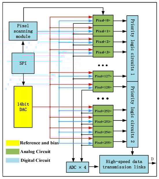
Figure 1.
Topmetal-CEE chip architecture block diagram.
The pixel unit contains an amplifier and a comparator. Since signals detected by the pixel unit is small, which is about tens of millivolt, it is necessary to provide a stable bias for the amplifier and an accurate reference voltage for the comparator. Moreover, the mismatch of the 256 pixel units need to be as small as possible, otherwise it will affect the imaging quality of the Topmetal-CEE chip, and thus DACs are needed for precise voltage adjustment. The DAC is required to provide bias voltages for 256 pixel units while considering factors such as routing capacitance and parasitic capacitance. Consequently, the DAC must possess ample driving capability to handle around a 10 pF load in total. To meet the stringent demands of precise and stable threshold and bias voltages within the Topmetal-CEE chip, a DAC with at least 12-bit of accuracy and minimal power consumption is essential. Ref. [7] presents a 12-bit digitally calibrated D/A converter that uses digital calibration to bring the design to a high level of accuracy, but its power consumption is high. The design proposed in [8] consumes less power, but its accuracy is only 4-bit. This work, tailored to the specific application requirements, incorporates Cadence tools for design and simulation. A DAC has been designed and fabricated, guaranteeing a stable output voltage with a precision of 14-bit over a range of 0–1.8 V, where the least significant bit (LSB) is a mere 101 μV.
2. Design of Key Modules
The DAC designed in this paper is required to bias the pixel unit. The types of DAC can be categorized into a switched-capacitor DAC, a delta-sigma DAC, and a resistive DAC. Switched-capacitor DACs have low-power characteristics, but in order to reduce the area of the DAC, their unit capacitance is generally in the fF order of magnitude, and small capacitance is difficult to match in tape-out, resulting in large errors. A delta-sigma DAC [9] is used as an oversampling DAC to achieve higher DAC accuracy by oversampling. Its internal structure contains an interpolation filter, a noise rectifier circuit, a DAC, and a low-pass filter. In order to ensure the quality of the over-sampled signal, the interpolation filter uses multiple filters to achieve a high sampling rate, and the increase in the number of bits of the quantizer also improves the accuracy of the DAC, which will increase power consumption and area. The resistive DAC includes a resistive network and an output amplifier, which is easier to guarantee the mismatch of the network and also can achieve a low power consumption. In summary, the resistive DAC is more suitable for this application. The typical structure of a binary-weighted resistive DAC is depicted in Figure 2. While this structure can be utilized in high-sampling-rate circuits due to its minimal susceptibility to the overall sampling caused by parasitic capacitance, it presents challenges during manufacture due to the significant impedance mismatch between the highest and lowest bits, reaching a ratio of 1:16384. This makes resistance matching difficult, whereby any mismatch introduced during layout design and production will undermine the performance of the DAC as data converters [10].
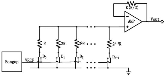
Figure 2.
Binary-weighted resistive DAC diagram.
The circuit suffers not only from the difficulty of matching the resistors, but also from the noise, and the one-sided spectral density of the thermal noise of the resistors can be expressed as
where Sv(f) is the thermal noise spectrum of the resistor, K is Boltzmann constant, T is the temperature in Kelvins, and R is the resistance value of the resistor. For the integrating noise P over 0–100 kHz at a temperature of 300 K, the noise can be expressed as
To achieve a high accuracy, the thermal noise should be kept below half of the least significant bit (LSB) value:
where R is the maximum resistance value in the resistive network and r is the minimum resistance value. Obviously, the smallest r is only 2.23 ohms, making it difficult to match the circuit during layout design. To solve this problem, the binary resistive DAC shown in Figure 3 has an improved structure, where the high and low bits are segmented by weighting the series resistors.
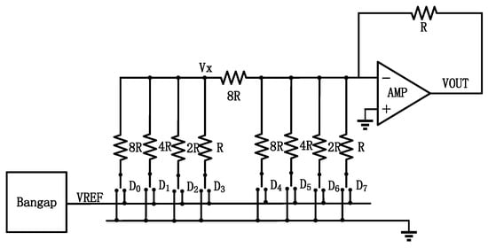
Figure 3.
The segmented DAC structure diagram.
In the following, we have analyzed the weight of the segmented resistors; when only the lowest bit is connected to the VREF, the higher six resistors are connected to the ground. The current of the feedback resistor R can be expressed as
The potential of Vx can be expressed as
The output voltage Vout can be expressed as
Similarly, other weighting bits can be obtained, and the total output expression can be expressed as
The above formula indicates that this method can reduce the resistance value from 27 to 23. However, if we want to achieve a resolution above a 14-bit DAC, this improvement still makes it difficult to match the design resistor network in the layout, resulting in relatively large errors. So, for this design, we have chosen an R-2R resistor network [11] structure to achieve a 14-bit voltage-type DAC, as illustrated in Figure 4. This R-2R structure exclusively uses two resistance values, R and 2R, significantly reducing the resistance values compared to the basic binary DAC architecture [12,13,14].
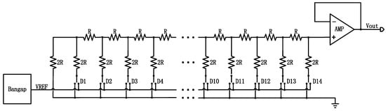
Figure 4.
The schematic of the proposed DAC overall structure diagram.
It comprises a bandgap reference, a 14-bit R-2R resistor network, and a differential operational amplifier working as a source follower. The bandgap reference operates at 3.3 V to produce a constant DC reference voltage of 1.8 V. The input code controls the switches within the R-2R resistor network to produce an output voltage at the terminal of the R-2R resistor network. The voltage is then buffered out by the source follower which is Vout, corresponding to the input code. The output voltage Vout of the DAC can be expressed as
2.1. Bandgap Reference Design
For an R-2R-type DAC, a stable voltage reference is imperative to ensure the precision and decide the full-scale range of the output voltage [15]. The low-voltage bandgap structure depicted in Figure 5 is the approach adopted in this study. This structure utilizes the technique of current summation at the positive and negative input nodes of the operational amplifier [16].
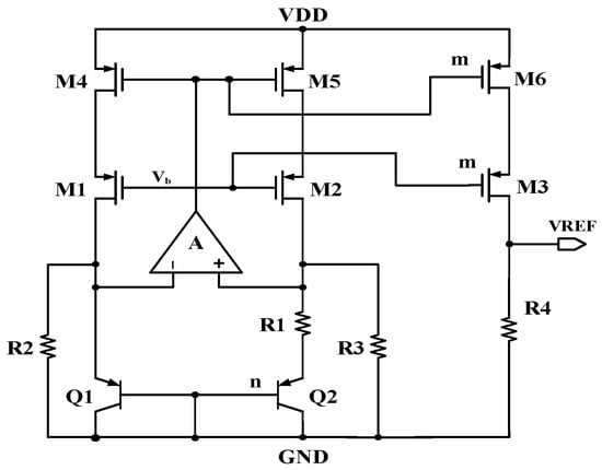
Figure 5.
The schematic of the proposed bandgap.
The voltage of the resistor R2 corresponds to the base and emitter of the bipolar transistor Q1 and is inversely proportional to temperature. Assuming that the resistors have zero-temperature resistance, the current flowing through R2 exhibits a negative temperature characteristic [17].
The output of the amplifier is connected to the gates of M4 and M5. There are two branches of positive and negative feedback in the BandGap loop, and the strength of negative feedback in the circuit should be greater than the strength of positive feedback to ensure the stability of the circuit [18].
The voltage formula across the terminals of R1 in Figure 5 is as follows:
Hence, the current flowing through resistor R1 is directly proportional to temperature. PMOS transistor M3, in conjunction with transistors M1 and M2, collectively forms a current mirror. M3 mirrors a current with two opposite temperature coefficients. By selecting the appropriate resistor ratio in the design process, a temperature-independent bandgap reference voltage is generated [19]. The pertinent derivation process is as follows:
where N is the ratio of the number of Q2 and Q1 transistors; VT = KT/q is a positive temperature coefficient voltage. The current flowing through resistor R4 is equal to the current flowing through M3, so the output voltage VREF of the bandgap is
Organize the above equation into the following:
The temperature drift coefficient (Tc) is as follows:
In the equation, Vmax, Vmin, and Vmean represent the maximum, minimum, and mean values of the reference voltage, respectively, while Tmax and Tmin denote the maximum and minimum temperature variations. A smaller temperature coefficient for the bandgap implies higher precision of the reference voltage, resulting in a better stable output voltage.
2.2. Circuit Design of the R-2R Resistor Network
The structure of an R-2R digital-to-analog converter inherently dictates that its precision is highly contingent upon the matching of the resistor network and switch matching. In other words, the actual resistance values of the vertical resistors and cross-bridge resistors are maintained at a two-fold relationship. In practical circuitry, linear-range-working NMOS transistors are used as the switch devices, and their on-resistance is given by
where Rs is the conductive resistance of the switch. For high-precision DAC, a large number of resistors and switches are required, and the increase in the number of resistors increases the chance of resistor mismatch, leading to a decrease in DAC accuracy [20]. Figure 6 illustrates the structure of a 14-bit analog-to-digital converter utilizing the R-2R resistor network design with offset switches for conduction resistance. Assuming that the resistance value of the resistor connected to the lowest switch D14 has changed to 2R + 2kR due to process deviation, the output voltage Vo of the DAC can be expressed as
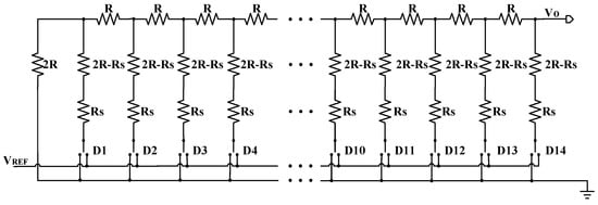
Figure 6.
Structure of the proposed R-2R resistor network.
This binary relationship is no longer established because of the switch resistance, thus reducing the resolution. All MOS switch transistors are set to the same dimensions, and the resistance values connected to the switches in the R-2R resistor network are reduced to satisfy the binary relationship. Assuming that the conduction resistance of the switches is Rs, the resistance value connected should be optimized to 2R-Rs, ensuring that the circuit adheres to the binary relationship [21,22].
The resistance of the lowest position of the R-2R structure is 2R, and according to Equation (3), the unit resistance r can be expressed as
This resistor value is less affected by the wires when designing the layout, making it easier to match.
2.3. Design of the Differential Operational Amplifier
In order to guarantee the DAC with sufficient driving capability, it is essential to add an operational amplifier at the voltage output of the weighted network, serving as the output stage for the DAC [23]. Typically, it is required that the error introduced by the DC gain should be less than the LSB of a 14-bit DAC. The gain error of the amplifier is approximately 1/AV, where AV represents the DC gain of the amplifier. Therefore, , ; taking into account the design specifications, a significant margin should be left, and the DC gain should exceed .
The settling time comprises two components: the large-signal settling time, which is contingent upon the slew rate; and the small-signal settling time, which is associated with the bandwidth of the amplifier [24]. The required settling time is 0.5 µs or less, particularly for large signals. Thus, a prescribed slew rate is necessitated for the amplifier as follows:
Considering the design criteria into account, it is advisable to maintain a certain margin, and the optimal design for the slew rate should exceed 5 V/µs.
The response time of an operational amplifier is within 7τ constants. The time constant is related to the unity-gain bandwidth (GBW), as follows:
Hence, the requirement is .
Thus, .
Considering the design requirement, it is advisable to retain a certain margin, and the optimal choice for the unity-gain bandwidth design is above 15 MHz. The DAC is used to provide the reference voltage to the pixel front-end of the whole matrix. The digital signals inside the pixel are very close to the front-end, which will increase the noise of the front-end because of the crosstalk. An amplifier with a large driving capability can reduce the noise of the references; thus, the amplifier still needs to have a certain driving capability.
According to the above requirements, considering the need to bias multiple pixel units, the amplifier adopts the ACBC three-stage amplifier design, with the structure shown in Figure 7 [25,26,27]. The first stage adopts a folded cascode structure, where M16 constitutes a buffer stage to avoid the large input capacitance affecting the operating speed of the circuit in Miller’s equivalent, the output stage adopts a class AB output, and M18 and M19 are used to control the DC bias voltage of the output stage.
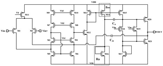
Figure 7.
ACBC three-stage amplifier schematic.
The circuit is modeled as shown in Figure 8, simplifying the stages into transconductance as well as load, the circuit is compensated using both feed-forward compensation as well as two-stage Miller compensation to ensure the phase margin of the amplifier [28].
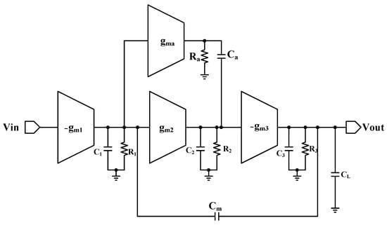
Figure 8.
ACBC three-stage amplifier structure.
The gain of the amplifier can be expressed as
The transfer function of the system can be expressed as
where each zero pole can be expressed as
The circuit has four poles and three zeroes. The first non-primary pole is equal to the first zero, then the effects of the zero and pole on the phase cancel each other out. The second non-primary pole can affect the phase margin, whereas when the second non-primary pole is located at twice the GBW, the phase margin can achieve 60 degrees.
3. Simulation, Layout, and Testing
3.1. Simulation
The chip is developed using the GSMC 180 nm CMOS process with a power supply voltage of 3.3 V.
3.1.1. Simulation of Bandgap Reference Circuit
The bandgap reference operates at a voltage of 3.3 V with a target output voltage of 1.8 V. It can be observed that the temperature drift coefficient is approximately 26.77 ppm/°C when the temperature varies from −40 °C to 85 °C. At room temperature, the output voltage is around 1.8003 V.
The simulated curves for the reference voltage under various process corners are depicted in Figure 9. Three distinct curves correspond to the TT, SS, and FF process corners, with respective temperature drift coefficients of 26.77 ppm/°C, 33.06 ppm/°C, and 27.7 ppm/°C. Table 1 presents the specific simulation results of the bandgap reference.
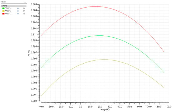
Figure 9.
Simulation results of reference voltage at TT, SS, and FF process corners.

Table 1.
Specific simulation results for bandgap reference at TT, SS, and FF process corners.
3.1.2. Simulation of the Differential Amplifier
Figure 10 illustrates the gain curves of the operational amplifier. It can be observed that the simulated gain of the operational amplifier is above 130 dB for the TT, FF, and SS process corners, meeting the 14-bit DAC requirements. Table 2 displays the corner simulation results for various amplifier specifications, whereby all of the specifications are acceptable.
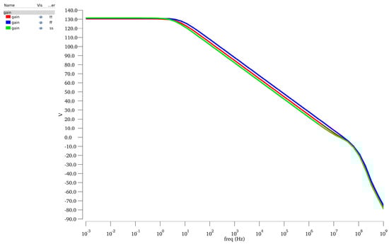
Figure 10.
Simulation results of operational amplifier gain.
Table 2.
Specific simulation results for amplifier reference at TT, SS, and FF process corners.
3.2. Layout and Post-Simulation
During the layout design, to reduce the mismatch, dummy resistors are used in the R-2R resistor network array [29,30]. The placement of the R-2R resistor network should strive for symmetry, wherein a parallel-then-series arrangement of multiple identical resistors is used [31,32].
The post-simulation results for DNL and INL analyses are depicted in Figure 11a,b, indicating that DNL is less than ±0.63 LSB, and INL is less than ±0.904 LSB.
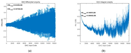
Figure 11.
(a) DNL analysis results for post-simulation of DAC; (b) INL analysis results for post-simulation of DAC.
3.3. Test Results
The DAC designed in this paper is fabricated using the GSMC 0.18 μm process, and the micrograph of the chip obtained after wafer fabrication is shown in Figure 12a,b.
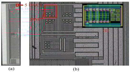
Figure 12.
(a) Die micrograph of the Topmetal_CEE; (b) die micrograph of the DAC; (c) layout of the DAC.
The DAC is integrated within the Topmetal-CEE chip. The test system setup comprises a PC, an FPGA board, the chip test board, and an oscilloscope. The PC conveys inputs to the Topmetal-CEE chip test board through the FPGA. A full binary code scan of the DAC output voltages is performed, recording the DAC output voltages. These results are then imported into MATLAB R2020b for DNL and INL analyses, as illustrated in Figure 13a,b. The test results indicate that the designed 14-bit DAC exhibits a DNL less than ±1.07 LSB and INL less than ±1.57 LSB. Additionally, the bandgap output is 1.799 V at room temperature with a temperature coefficient of 48.25 ppm/°C.
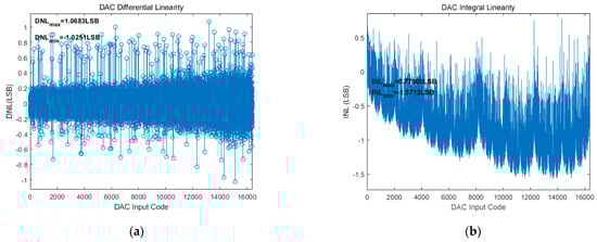
Figure 13.
(a) DNL analysis of DAC test results; (b) INL analysis of DAC test results.
Table 3 shows the parameter comparison between the DAC in this design and the related references. The DAC in this paper is designed with higher accuracy and better synthesized parameters compared to the circuits in [31,32].
Table 3.
Overall performance comparison.
4. Conclusions
To meet the stringent precision requirements for a bias voltage in the Topmetal-CEE chip, a high-precision integrated DAC is realized. In the design, a low-voltage bandgap structure is designed to enhance the stability and a high-performance buffer is used to enhance its driving capability. An R-2R resistor network with switch resistance matching is used to improve the accuracy of the DAC. The test results reveal that the DAC chip, operating at a 3.3 V power supply voltage, can realize output voltages ranging from 0 to 1.8 V. The differential non-linearity error is less than 1.07 LSB, and the integral non-linearity is less than 1.57 LSB. The test results are as expected.
Author Contributions
Conceptualization, Y.D. and P.Y.; methodology, Z.S.; formal analysis, J.L.; resources, G.H.; data curation, Z.R. and Y.F.; writing—original draft preparation, Y.D. All authors have read and agreed to the published version of the manuscript.
Funding
This research was funded by the National Natural Science Foundation of China grant number 12075100 and 11905186. And this research was funded by the National Key Research and Development Program of China grant number 2022YFA1602103. The APC was funded by Central China Normal University.
Data Availability Statement
No new data were created.
Conflicts of Interest
The authors declare no conflict of interest.
References
- Zhan, W.L.; Xia, J.W.; Zhao, H.W.; Xiao, G.Q.; Yuan, Y.J.; Xu, H.S.; Man, K.D.; Yuan, P.; Gao, D.Q.; Yang, X.T.; et al. HIRFL today. Nucl. Phys. A 2008, 805, 533c–540c. [Google Scholar] [CrossRef]
- Zhan, W.; Xu, H.; Sun, Z.; Xiao, G.; Xia, J.; Zhao, H.; Song, M.; Yuan, Y.; Hirfl-Csr Group. Present status of HIRFL in Lanzhou. Int. J. Mod. Phys. E 2006, 15, 1941–1956. [Google Scholar] [CrossRef]
- Xiao, Z.G.; Yong, G.C.; Chen, L.W.; Li, B.-A.; Zhang, M.; Xiao, G.-Q.; Xu, N. Probing nuclear symmetry energy at high densities using pion, kaon, eta and photon productions in heavy-ion collisions. Eur. Phys. J. A 2014, 50, 37. [Google Scholar] [CrossRef]
- Zhu, Y.; Shyam, K.; Hu, C.; Chen, Z.; Zhang, Y.; Zhao, F.; Wei, X.; Duan, L.; Xu, N.; Qiu, H. Cluster reconstruction for the CSR External-target Experiment (CEE) time projection chamber. Nucl. Phys. Rev. 2021, 38, 416–422. [Google Scholar]
- You, B.; Gao, C.; Yang, P.; Guo, D.; Tian, X.; Huang, G.; Liu, J.; Sun, X.; Wang, H.; Xiao, L. The Topmetal-CEE prototype, a direct charge sensor for the beam monitor of the CSR external-target experiment. J. Instrum. 2022, 17, C09030. [Google Scholar] [CrossRef]
- Wang, H.-L.; Wang, Z.; Gao, C.-S.; Liao, J.-W.; Sun, X.-M.; Yang, H.-B.; Zhao, C.-X.; Liu, J.; Ma, P.; Li, Z.-L.; et al. Design and tests of the prototype beam monitor of the CSR external target experiment. Nucl. Sci. Tech. 2022, 33, 36. [Google Scholar] [CrossRef]
- Liu, H.; Xu, L.; Tian, T. A monolithic 12-bit digitally calibrated D/A converter. IEICE Electron. Express 2021, 18, 20200371. [Google Scholar] [CrossRef]
- Prasad, S.R.; Sree, N.K.; Omkumar, K.; Srujana, K. An Efficient and Low Power 45nm CMOS Based R-2R DAC. In Proceedings of the 2023 4th International Conference for Emerging Technology (INCET), Belgaum, India, 26–28 May 2023; pp. 1–6. [Google Scholar] [CrossRef]
- Pavan, S.; Schreier, R.; Temes, G.C. Understanding Delta-Sigma Data Converters; John Wiley & Sons: Hoboken, NJ, USA, 2017. [Google Scholar]
- Maloberti, F. Data Converters Specifications; Springer: Boston, MA, USA, 2007. [Google Scholar]
- Smith, B.D. Coding by feedback methods. Proc. IRE 1953, 41, 1053–1058. [Google Scholar] [CrossRef]
- Li, Y.; Zeng, T.; Chen, D. A high resolution and high accuracy R-2R DAC based on ordered element matching. In Proceedings of the IEEE International Symposium on Circuits and Systems (ISCAS), Beijing, China, 19–23 May 2013; pp. 1974–1977. [Google Scholar]
- Kim, K.D.; Park, C.B.; Lee, S.W.; Park, G.-S.; Cho, G.-H.; Kim, J.; Kim, J.; Choi, Y.-K.; Kim, J.; Hwang, G.; et al. 35.3: A 10-Bit Linear R-string DAC Architecture for Mobile Full-HD AMOLED Driver ICs; SID Symposium Digest of Technical Papers; Blackwell Publishing Ltd.: Oxford, UK, 2013; Volume 44, pp. 469–472. [Google Scholar]
- Enuchenko, M.S.; Morozov, D.V.; Pilipko, M.M. An 8-bit parallel DAC with segmented architecture. J. Commun. Technol. Electron. 2017, 62, 89–100. [Google Scholar] [CrossRef]
- Jun, S. Optimization of Bandgap Reference with High PSRR on Deep Submicron. In Proceedings of the 2021 IEEE International Conference on Consumer Electronics and Computer Engineering (ICCECE), Guangzhou, China, 15–17 January 2021; pp. 148–153. [Google Scholar]
- Banba, H.; Shiga, H.; Umezawa, A.; Miyaba, T.; Tanzawa, T.; Atsumi, S.; Sakui, K. A CMOS bandgap reference circuit with sub-1-V operation. IEEE J. Solid-State Circuits 1999, 34, 670–674. [Google Scholar] [CrossRef]
- Yang, H.; Wu, C. An LDO Circuit Design Based on On-chip Compensation. J. Phys. Conf. Ser. IOP Publ. 2022, 2383, 012044. [Google Scholar] [CrossRef]
- Liu, N.; Geiger, R.; Chen, D. Bandgap voltage v go extraction with two-temperature trimming for designing sub-ppm/°C voltage references. In Proceedings of the 2019 IEEE International Symposium on Circuits and Systems (ISCAS), Sapporo, Japan, 26–29 May 2019; pp. 1–4. [Google Scholar]
- Ebenezer, P.S.; Naganadhan, V.; Chen, D.; Geiger, R. Three-Junction Bandgap Circuit with Sub 1 ppm/°C Temperature Coefficient. In Proceedings of the 2020 IEEE 63rd International Midwest Symposium on Circuits and Systems (MWSCAS), Springfield, MA, USA, 9–12 August 2020; pp. 305–308. [Google Scholar]
- Saponara, S.; Baldetti, T.; Fanucci, L.; Volpi, E.; D’Ascoli, F. High-level modeling of resistor string based digital-to-analog converters. Analog. Integr. Circuits Signal Process. 2011, 66, 407–416. [Google Scholar] [CrossRef]
- Kazeminia, S.; Hesamiafshar, Y.; Hadidi, K.; Khoei, A. On matching properties of R-2R ladders in high performance digital-to-analog converters. In Proceedings of the 2010 18th Iranian Conference on Electrical Engineering, Isfahan, Iran, 11–13 May 2010; pp. 432–436. [Google Scholar]
- Razavi, B. The R-2R and C-2C ladders [A circuit for all seasons]. IEEE Solid-State Circuits Mag. 2019, 11, 10–15. [Google Scholar] [CrossRef]
- Wu, T.Y.; Jih, C.T.; Chen, J.C.; Wu, C.Y. A low glitch 10-bit 75-MHz CMOS video D/A converter. IEEE J. Solid-State Circuits 1995, 30, 68–72. [Google Scholar] [CrossRef]
- Li, H.G.; Yin, X.Y.; Zhang, Z.Y. High-precision mixed modulation DAC for an 8-bit AMOLED driver IC. J. Disp. Technol. 2015, 11, 423–429. [Google Scholar] [CrossRef]
- Qin, C.; Zhang, L.; Zhou, C.; Zhang, L.; Wang, Y.; Yu, Z. Dual AC boosting compensation scheme for multistage amplifiers. IEEE Trans. Circuits Syst. II Express Briefs 2016, 64, 882–886. [Google Scholar] [CrossRef]
- Chaddad, A. Low-noise front-end receiver dedicated to biomedical devices: NIRS acquisition system. Circuits Syst. 2014, 2014, 191–200. [Google Scholar] [CrossRef]
- Tiwari, R.K.; Mishra, G.R.; Misra, M. A new high performance CMOS differential amplifier. Int. J. Electron. Eng. Res. 2009, 1, 147–154. [Google Scholar]
- Sansen, W.M. Analog Design Essentials; Springer Science & Business Media: New York, NY, USA, 2007. [Google Scholar]
- Lee, H.; Park, S.; Kim, J.; Kim, C. A 6-bit 2.5-GS/s time-interleaved analog-to-digital converter using resistor-array sharing digital-to-analog converter. IEEE Trans. Very Large Scale Integr. (VLSI) Syst. 2014, 23, 2371–2383. [Google Scholar] [CrossRef]
- Kouda, S.; Kodama, C.; Fujiyoshi, K. Improved method of cell placement with symmetry constraints for analog IC layout design. In Proceedings of the 2006 International Symposium on Physical Design, San Jose, CA, USA, 9–12 April 2006; pp. 192–199. [Google Scholar]
- Lin, Y.; Geiger, R. Resistors layout for enhancing yield of R-2R DACs. In Proceedings of the 2002 IEEE International Symposium on Circuits and Systems (ISCAS), Phoenix-Scottsdale, AZ, USA, 26–29 May 2002; p. V. [Google Scholar] [CrossRef]
- Graupner, A.; Jancke, R.; Wittmann, R. Generator based approach for analog circuit and layout design and optimization. In Proceedings of the 2011 Design, Automation & Test in Europe, Grenoble, France, 14–18 March 2011; pp. 1–6. [Google Scholar]
- Arbet, D.; Nagy, G.; Stopjaková, V.; Gyepes, G. A self-calibrated binary weighted DAC in 90nm CMOS technology. In Proceedings of the 2014 29th International Conference on Microelectronics Proceedings-MIEL 2014, Belgrade, Serbia, 12–14 May 2014; pp. 383–386. [Google Scholar]
- Sekyere, M.; Darko, E.N.; Bruce, I.; Chen, D. Ultra-Small Area, Highly Linear Sub-Radix R-2R Digital-To-Analog Converters with Novel Calibration Algorithm. In Proceedings of the 2023 IEEE 66th International Midwest Symposium on Circuits and Systems (MWSCAS), Phoenix, AZ, USA, 6–9 August 2023; pp. 604–608. [Google Scholar]


Disclaimer/Publisher’s Note: The statements, opinions and data contained in all publications are solely those of the individual author(s) and contributor(s) and not of MDPI and/or the editor(s). MDPI and/or the editor(s) disclaim responsibility for any injury to people or property resulting from any ideas, methods, instructions or products referred to in the content. |
© 2024 by the authors. Licensee MDPI, Basel, Switzerland. This article is an open access article distributed under the terms and conditions of the Creative Commons Attribution (CC BY) license (https://creativecommons.org/licenses/by/4.0/).