Abstract
Board milling is one of the most widespread methods for manufacturing printed circuit boards from low frequencies to the microwave and millimeter wave range. In this contribution, the detrimental effect of defects typical of printed circuit board plotters has been investigated. In detail, a systematic frequency shift in the circuit performance has been observed both in terms of S21 and S11 parameters. The performance degradation has been analyzed and attributed to the inaccurate milling depth, which is typical of many plotters, particularly for less recent models. After the conductor removal step, the unwanted milling of dielectric material changes the electrical properties of the microstrip structure, in turn affecting the circuit performance. This circumstance has been investigated by means of electromagnetic simulations performed on the real case study of a parallel coupled lines filter. Therefore, a filter prototype has been realized and measured to confirm the simulated results. This study can be beneficial to those professionals involved in the design and realization of microwave and millimeter waves circuits with board milling machines.
1. Introduction
A great effort by the scientific community has always been directed toward the design of increasingly higher-performance electronic circuit boards. To design a high-quality board, it is mandatory to achieve a good correspondence between the expected, i.e., simulated, and the real, i.e., measured, performance. This is particularly true for microwave and millimeter wave components whereby the physical characteristics of the transmission lines have a great impact and, indeed, are exploited to achieve the desired electrical behavior [1,2,3,4,5,6].
Different options are available to realize microwave circuits [7]. Classic and more consolidated technologies rely on subtractive techniques. In detail, the starting material is a layer of insulating material with a conductor plating on both sides. Printed circuit board (PCB) milling or laser-based machines can be exploited to remove the conductive layer where it is not required. Recently, additive processes are attracting the interest of the community. Unlike subtractive techniques, the starting material is only a layer of insulating material without any conductive sheet, and by exploiting inkjet printing, a conductive ink is deposited where the conductive line is required [8].
Although additive techniques are currently already effective and promising for future board manufacturing, the classic subtractive techniques are still the most widely employed.
Despite the great technological progress in the field, many plotters, especially the older ones, are characterized by well-known and unpredictable inaccuracies that, if not adequately addressed, can seriously affect the performance of the circuits [9].
Several researchers have tried to deal with the possible issues arising from the prototyping process that, in turn, affect the correlation between simulation and measurement. In [10], the authors analyzed the tolerance sensitivity in substrate integrated waveguide components. They extracted a parametric electrical model able to account for the effect of small variations in the geometry of the component due to the manufacturing process. They selected a real case study of two filters fabricated in substrate integrated waveguide and microstrip technology with the task to assist the design process.
Instead, [11] mainly focused on investigating the variation of the dielectric constant for 3D-printed circuits. In this case, the authors tried to compensate the variation by implementing a post-fabrication technique. The frequency shift of the scattering parameters is the main effect observed for a microstrip patch antenna.
In [12], the authors verified the repeatability of filter manufacturing due to process errors that, in turn, involve a significant shift of the frequency response. They realized seven replicas of a coupled-line bandpass filter, the same filter analyzed in this article, to be measured under the same testing conditions, showing a higher sensitivity of the reflection parameters to manufacturing tolerances and connector realization, along with a lower sensitivity of the transmission parameters.
In this context, it is essential to investigate how the inaccuracies of the fabrication process can affect the performance of the circuit.
Although some researchers have tried to perform sensitivity analysis based on the most common defects, this is the first work whereby the effect of an excessive milling depth, typical of many plotters, is taken into account. This inaccuracy involves a typical but systematic frequency shift in the circuit performance, reproducing an effect similar to that of a dielectric constant decrease. First, this scenario was theoretically analyzed and described and, thereafter, investigated by means of electromagnetic simulations performed on the real case study of a parallel coupled lines filter.
The cited contributions are very interesting for the scientific community, but usually, the state-of-art methods lack a detailed description about the source of unpredictable inaccuracies. Indeed, it is not uncommon to read about structural issues in microwave components due to the mechanical flaws during the fabrication process of the component itself. Very often, the possible defect sources are not clarified and, especially, their real effect is not detailed. As a consequence, all the researchers are aware that the measured results are destined to be different compared to the simulated ones. This paper wants to describe one of the possible sources that involves the unpredictable inaccuracies in a clear and precise manner. In other words, this contribution aims to cover the absence of a detailed description of the impact of an excessive milling depth, which is the main cause of the shifted frequency response.
The effect has been modeled by a modified microstrip structure, and a filter prototype has been realized and tested to confirm the simulated geometry. In addition, this study is beneficial for a plethora of applications whereby an accurate and precise correspondence between simulations and measurements on prototypes working at microwave frequencies is required [13,14,15,16,17,18,19,20].
The main contributions of the article can be synthetized as follows:
- the effect of an excessive plotter milling depth has been investigated for the first time;
- the typical frequency shift in the circuit performance has been modeled as a dielectric constant decrease;
- the scenario has been simulated to validate the theoretical analysis;
- finally, the hypothesis has been experimentally validated by realizing a filter prototype.
The paper is organized as follows. The microwave structure alteration due to the defect is described in Section 2. Section 3 shows the steps required to design the case study of a microstrip parallel coupled lines filter. Finally, the simulation and measurement of the component are disclosed in Section 4, whereas the results are analyzed in Section 5. The conclusions are drawn in Section 6.
2. Microstrip Structure Alteration Due to Defects
The structure of microstrip lines is very popular due to some beneficial features, such as being lightweight, the ease of integration, and miniaturization. Geometrically, it is composed by a conductor of length L and width W on a grounded dielectric substrate mainly characterized by relative permittivity and thickness h [21]. Most of the field lines are in the dielectric volume between the conductor and the ground plane, whereas some fraction is in the air region above the microstrip. Since the waves travel in an inhomogeneous medium, the propagation velocity is affected by the influence of both media, and the effective speed is a value ranging from the speed of electromagnetic waves traveling in the substrate to their speed in air. Although the microstrip lines support fields featuring a hybrid transverse electric (TE)–transverse magnetic (TM) wave, in many practical applications, the quasi-static approximation (quasi-TEM) can be considered, because the substrate thickness is tiny compared to the wavelength and the characteristic impedance. In addition, the propagation constant and phase velocity can be expressed in terms of the effective dielectric constant . An approximate expression of is reported in (1), which corresponds to Equation (3.195) in [21].
During the milling process, the unwanted conductor is removed where it is not required by means of a set of suitable milling tools. Theoretically, only the conductor should be removed, without deteriorating the substrate at the interface. However, if the milling depth is inaccurate, after the conductor removal step, additional dielectric material might also be removed, changing the electrical properties of the microstrip structure and, in turn, affecting the circuit performance. Indeed, an inaccurate milling depth involves a substantial alteration of the circuit’s S21 and S11 due to the modified structure. It is well known that the research of a particular structure could fit the requested performance. For instance, in [22], the authors analyzed the impact of different patch antenna shapes as concerns the antenna’s characteristics itself. In addition, the optimization-driven parameter stage is fundamental during the design of every component, as highlighted in [23]. In most cases, this stage is conducted by parametric studies, and this may not be sufficient, thus requiring the application of rigorous numerical methods. Therefore, these contributions underline how the structure modification affects the performance metrics, whereas this paper examines how the performance itself is conditioned by unwanted geometrical modifications of the component.
As a direct consequence of the new modified structure due to the excessive milling depth, a new value of the effective dielectric constant, can be considered. It assumes a value lower than because the strip is surrounded by a larger volume of air than the expected one. Therefore, assumes a value between the air dielectric constant and .
It is worth noting that an analytic estimate of is very challenging without knowing a priori the extent of the machine error. Indeed, with reference to (1), it is not only a matter of changing h, but the entire structure is modified.
A possible strategy consists of simulating the new geometry with the aim to predict the behavior of the real circuit, thus making the design of microwave circuits more effective, and this is the task of the next section.
3. Parallel Coupled Lines Filter Design
In order to test the effectiveness of the model, a real case study has been considered. In detail, a parallel coupled lines filter has been designed and simulated according to the modified microstrip structure described in the previous section.
The parallel coupled lines filter has been designed to obtain a bandpass Butterworth response within a bandwidth of 5 GHz–6 GHz. The Insertion Loss method has been employed, whereas 5 elements have been considered for the filter design. The admittance inverter constants have been calculated according to (2)–(4), which correspond to Equations (5.73a–5.73c) in [24].
where , ,…, are the elements of the low-pass prototype with a normalized cut-off frequency, FBW is the fractional bandwidth of the bandpass filter, are the characteristic admittances of the J-inverters, and is the characteristic admittance corresponding to 50 Ω.
Thereafter, the odd-mode and even-mode impedances are calculated as follows in (5) and (6), extracted (or extrapolated) from (5.74a–5.74b) in [24].
The adopted substrate is the hydrocarbon ceramic laminate RO4003C by Rogers Corporation®, characterized by a process dielectric constant of 3.38, design dielectric constant of 3.55, dissipation factor tan δ of 0.0027, and dielectric thickness of 1524 μm. The thickness of the conductor is 17.5 μm.
The physical width Wj, length Lj, and spacing S of the resonators have been calculated accordingly and optimized. The final values are reported in Table 1.

Table 1.
Physical dimensions of the parallel coupled lines filter.
Since the available 3.5 mm coaxial connectors require a line width smaller than the width corresponding to the characteristic impedance of 50 Ω, a matching network has been added at both ports of the filter to accomplish both the geometrical requirements of the connector and maintaining the proper input and output reflection coefficients.
4. Simulation and Measurement of the Component
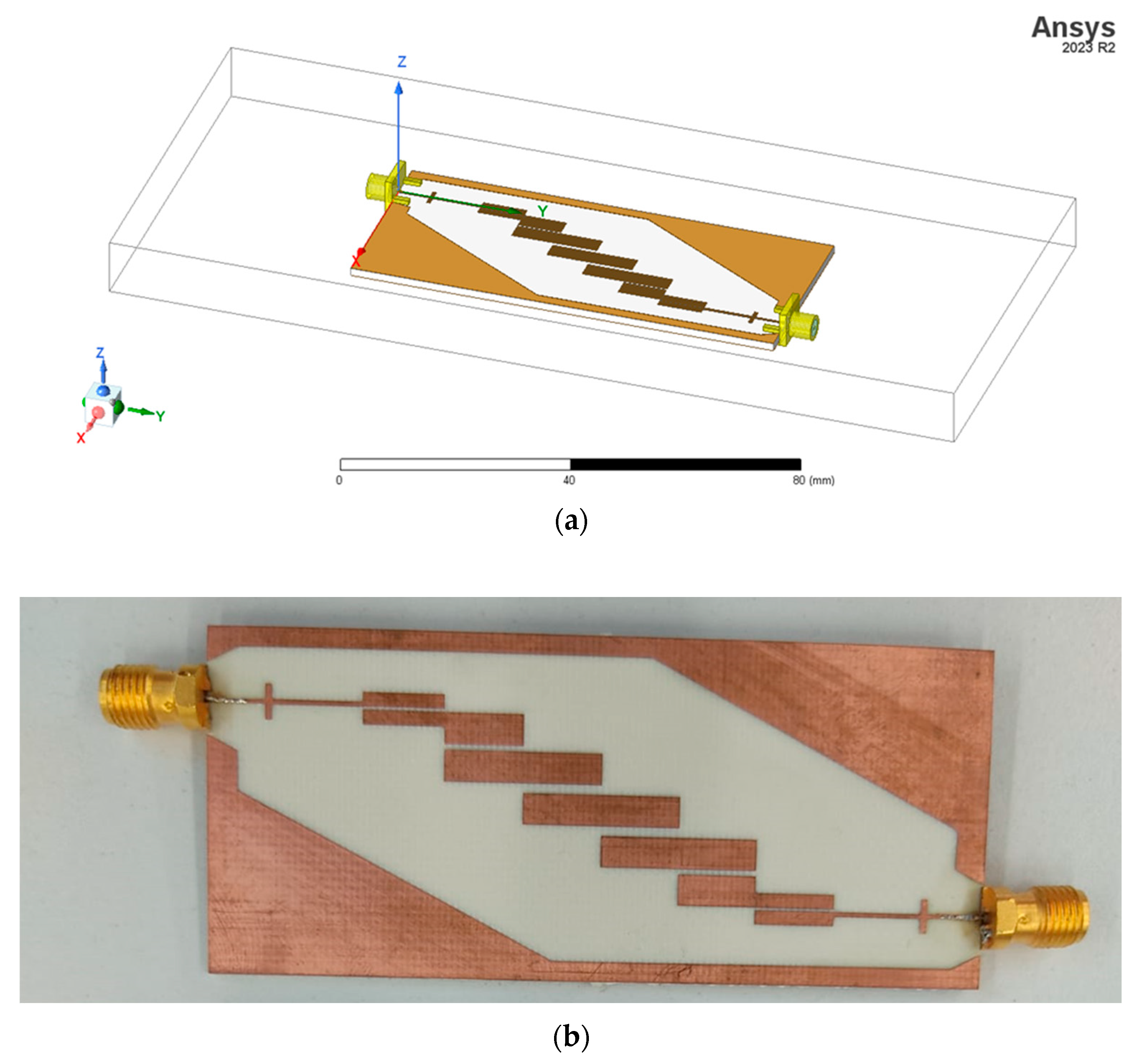
Initially, the filter was designed by considering the classic microstrip structure. It was simulated by using the HFSS Electromagnetic Suite within Ansys®. In Figure 1a, the 3D layout of the simulated filter, including the two connectors, is shown, whereas a picture of the prototype is reported in Figure 1b. It shows the correspondence between the simulated and realized filter prototypes.

Figure 1.
(a) Layout and (b) picture of the bandpass parallel coupled lines filter.
According to the available filter substrate, the RO4003C dielectric has been simulated by setting a dielectric constant of 3.55, a dissipation factor tan δ of 0.0027, and dielectric thickness of 1524 μm. The thickness of the conductor is 17.5 μm. A perfect electrical conductor (PEC) has been used for both the protype metals and for the connector conductive sections. Perfect E boundaries are associated with the conductive elements, whereas a radiation boundary envelops all the prototype. Lumped 50 Ω ports were used in the simulations.
The component was manufactured by using a high-precision mechanical plotter S103 Protomat by LPKF Laser & Electronics SE.
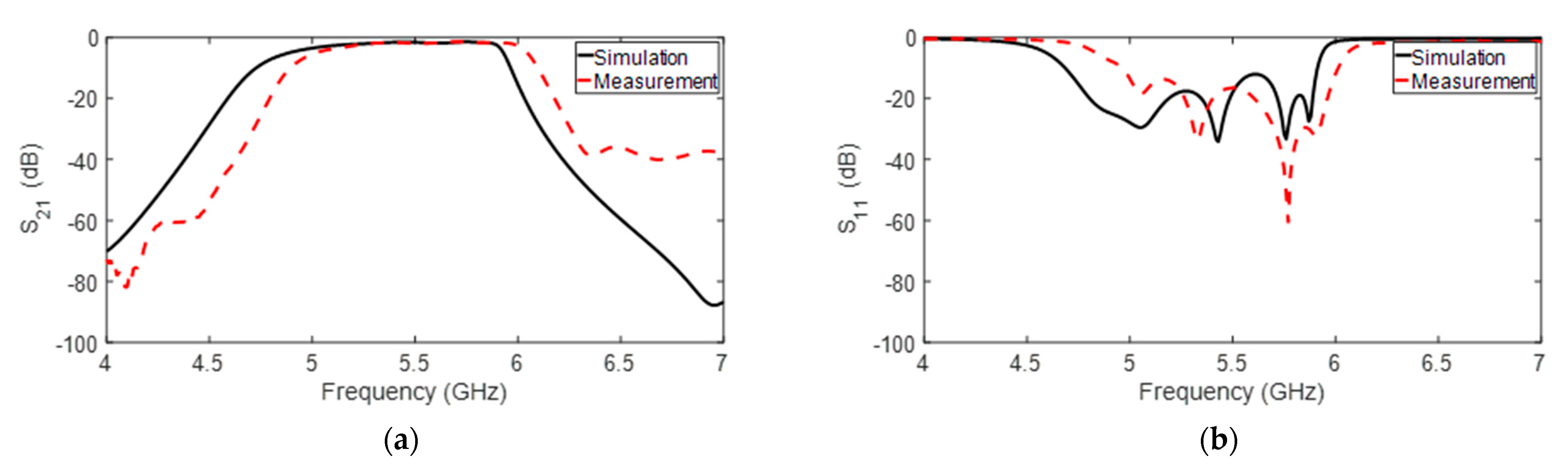
The performance comparison between the simulated and measured results is shown in Figure 2. Although the simulation process can be considered quite accurate due to the known very good performance of the current electromagnetic simulators and high level of details of the reproduced geometry, including the effects of the connectors, a frequency shift can clearly be noticed.
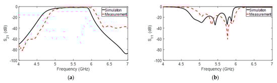
Figure 2.
Comparison between the simulated (black solid line) and measured (red dashed line) (a) S21 and (b) S11 of the bandpass parallel coupled lines filter.
The right-shift of the frequency can be attributed to a dielectric constant lower than expected. Indeed, according to (7), which is derived from (3.193) in [21], after fixing the physical length of the microstrip , the operating frequency is inversely proportional to the effective dielectric constant.
However, whereas the effective dielectric constant can behave, as it was higher than the expected value, e.g., due to processing residues being left on the circuit or circuit fabrication defects, there are very few events that make a circuit appear as if it has a lower effective dielectric constant.
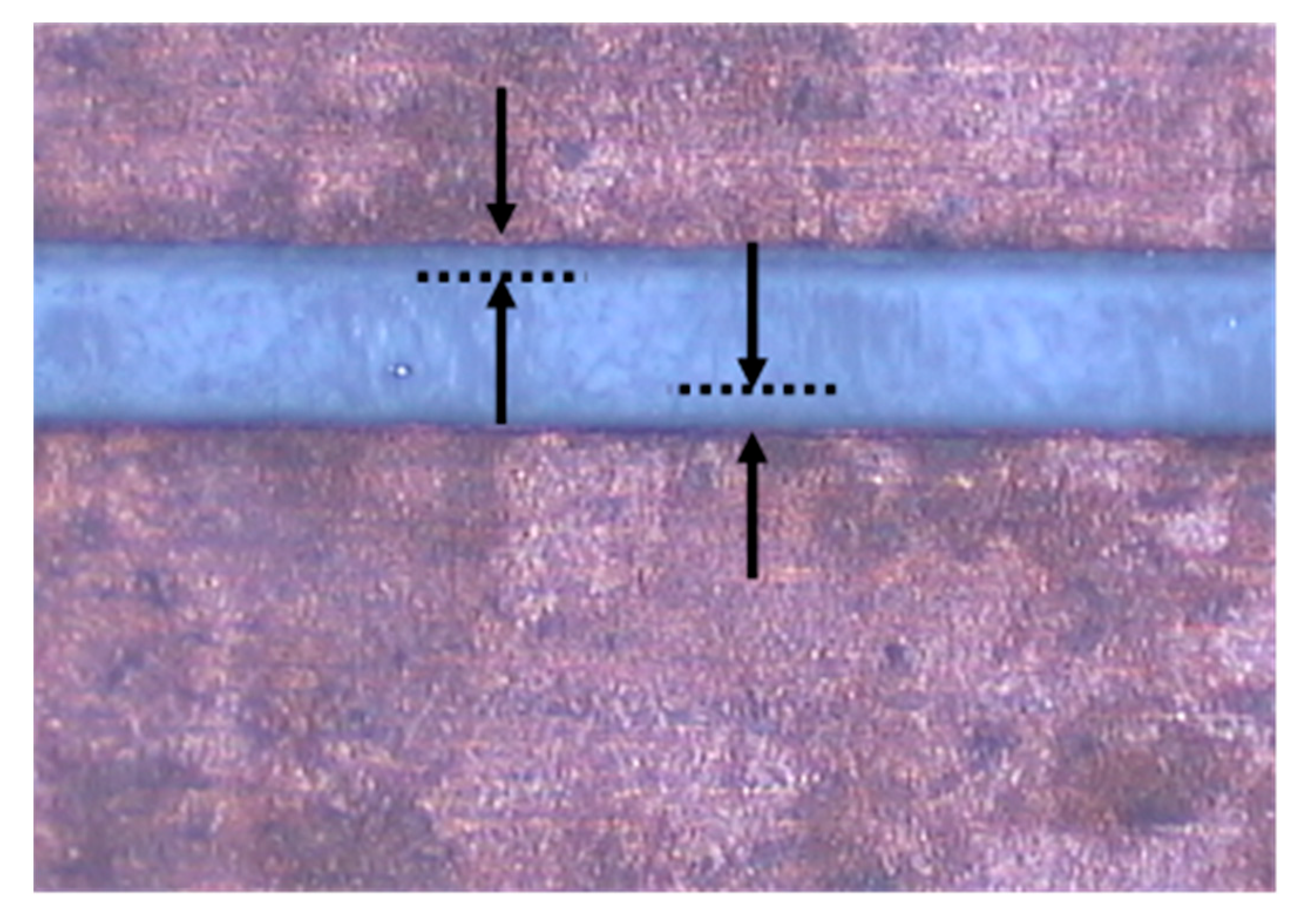
On the other hand, according to Section 2, the trench created by the higher milling depth can lower the effective dielectric constant by increasing the volume of air near the conductor. This statement cannot be noticed without having a cross-sectional view of the board. However, if there is a trench, the light by the conductor can be distorted by the trench creating the shading visible in Figure 3.
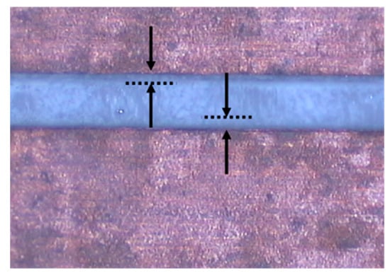
Figure 3.
Details of the prototype layout.
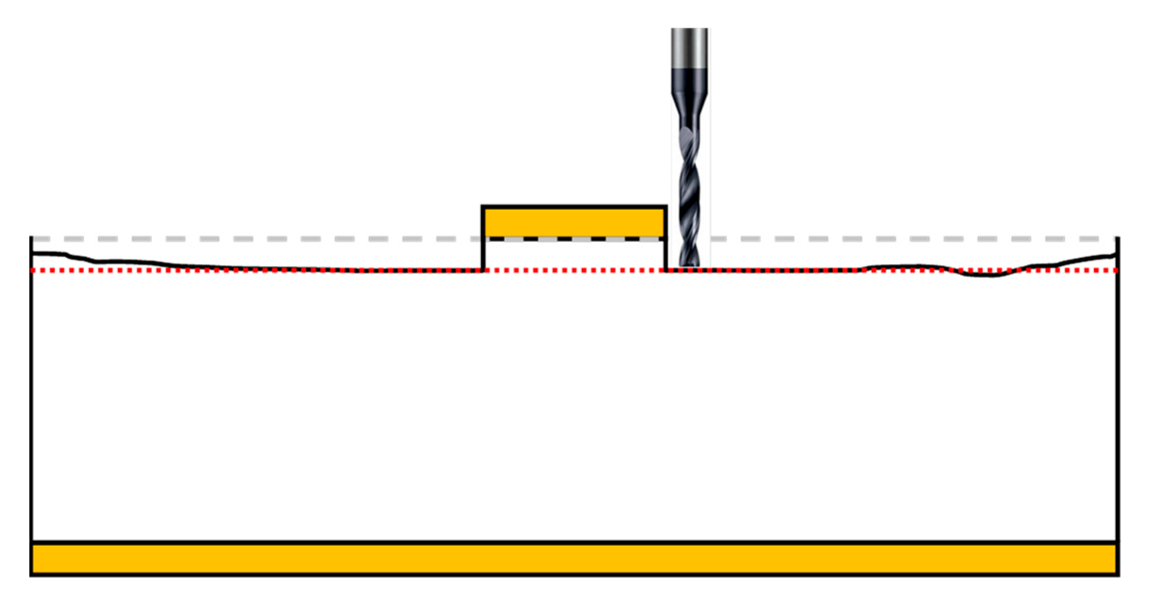
In order to take into account the effect of this substrate defect, a modified geometry of the substrate has been considered, according to the sketch shown in Figure 4, whereby the grey dashed line represents the original substrate level, and the black solid line is the new substrate top level.
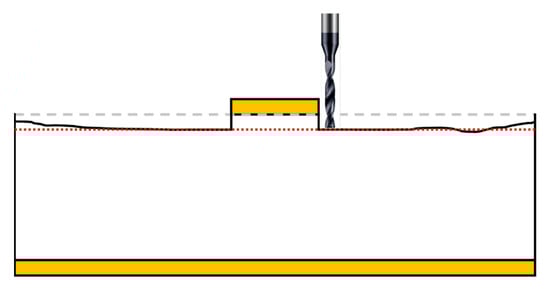
Figure 4.
Geometry of the microstrip line in the case of an excessive milling depth during the circuit fabrication. The grey dashed line represents the original substrate level, the black solid line is a sketch of a possible new substrate top level, and the red dotted line is the new substrate top level considered in the electromagnetic simulation.
Although possible in theory, it is quite impractical simulating so irregular a surface in electromagnetic simulators, which, in any case, would require the accurate knowledge of the board surface profile. Therefore, the defect has been modeled in the electromagnetic simulator as the new substrate top level, depicted with the red dotted line in Figure 4.
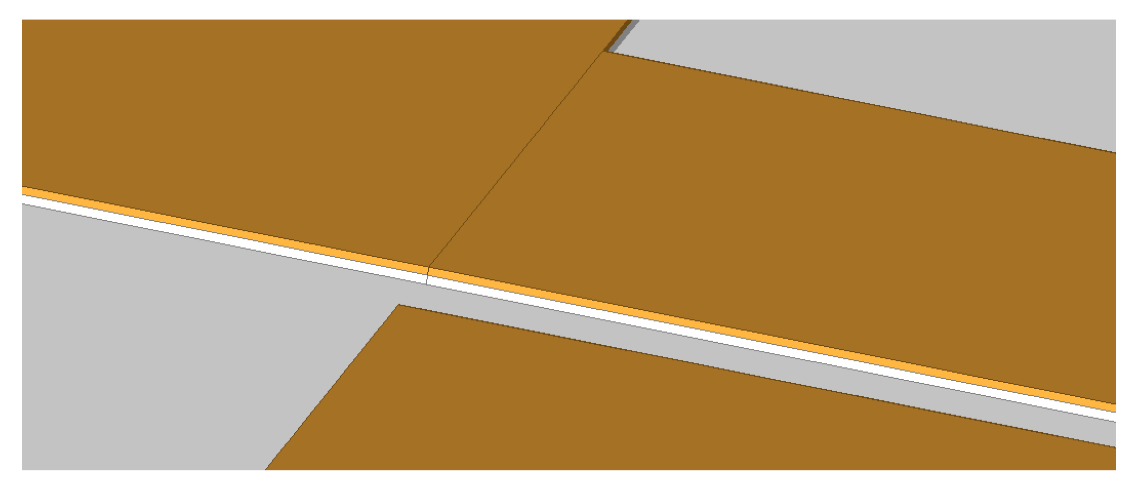
The details of the geometry can be observed in Figure 5, where the tiny residual layer of the dielectric is present under the copper layer.
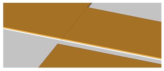
Figure 5.
Details of the filter layout reproduced in the electromagnetic simulator.
5. Experimental Results
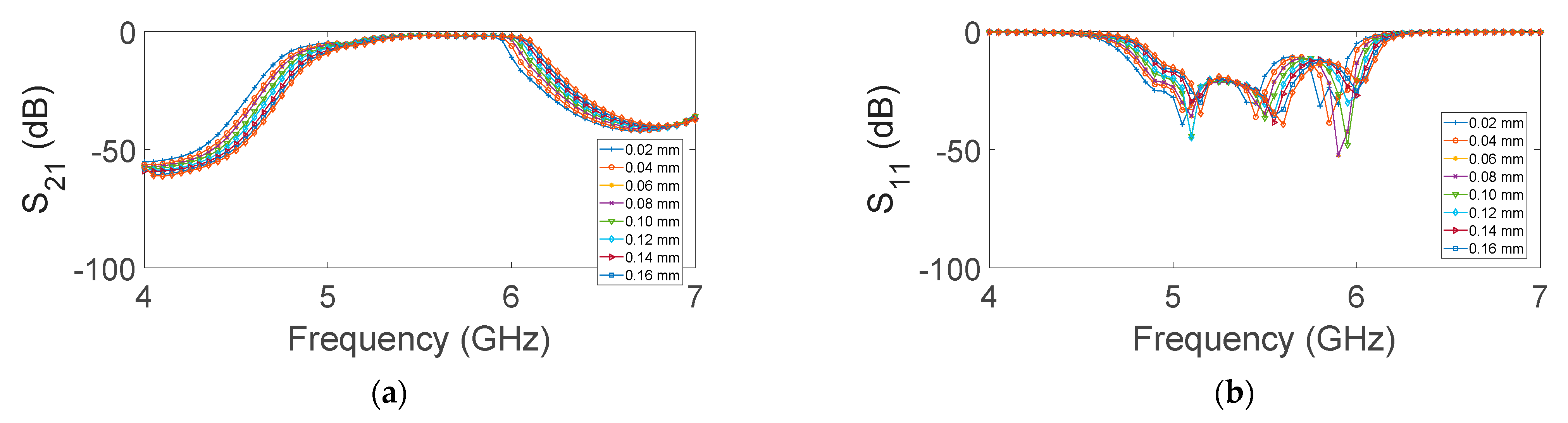
A key parameter of the model is represented by the additional milling depth to be considered in the simulation. As already anticipated, measuring the accurate real depth is a challenging task. Moreover, even if possible, measuring the additional milling depth would not be so useful for the scientific and professional community, because the tools required to perform the measurement are not ordinarily available in many research laboratories. Therefore, it would be more interesting trying to evaluate a suitable milling depth by exploiting the electromagnetic simulator, a procedure that can be reproduced by the interested researchers. To this aim, a parametric analysis has been conducted by varying the additional milling depth from 0.02 mm to 0.16 mm. The resulting scattering parameters can be observed in Figure 6.
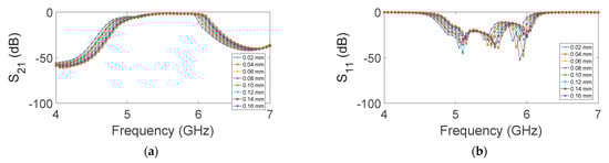
Figure 6.
Simulated (a) S21 and (b) S11 of the bandpass parallel coupled lines filter by varying the additional milling depth from 0.02 mm to 0.16 mm.
It is worth noting that, as theoretically expected, the effect of varying the additional milling depth involves a shift of the circuit operating frequency, i.e., the bandwidth for the case of a bandpass filter. This is an interesting result, because very often, the main difference between simulated and measured results consists of a frequency shift that, due to the great quantity of possible variables, is very difficult to explain.
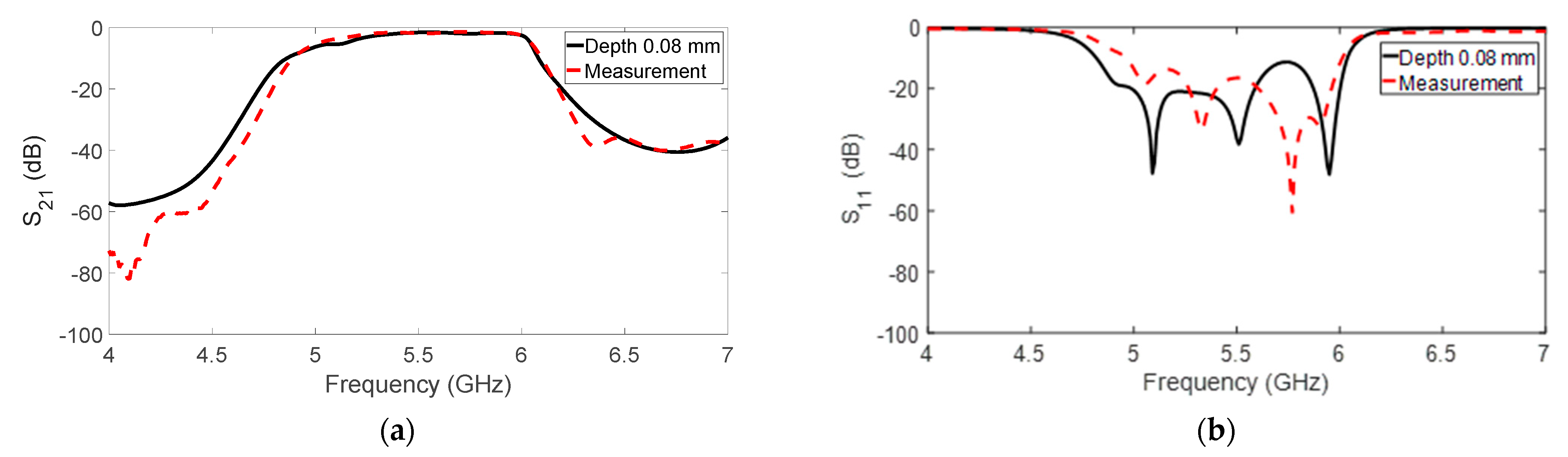
Thereafter, the results of the parametric simulation were compared to the real measurements. The simulation considering the additional milling depth of 0.08 mm was selected as the most appropriate and near to the real filter behavior.
A comparison between measured scattering parameters and the simulated ones of the modified structure is shown in Figure 7.
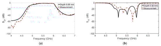
Figure 7.
Comparison between the simulated geometry with an additional milling depth (black solid line) and measured data (red dashed line). (a) S21 and (b) S11 of the bandpass parallel coupled lines filter.
It is possible to note the good correspondence between the measured and simulated data concerning both the S21 and S11 parameters and the complete suppression of the frequency shift.
6. Conclusions
In this contribution, the effect of an inaccurate milling depth for printed circuit board plotters has been investigated. In detail, a frequency shift in the frequency behavior of microwave circuits has been observed and investigated. The main effects are attributed to the modification of the classic microstrip geometry that, in turn, involves a change in the effective dielectric constant and in the electrical properties of the structure. This circumstance has been modeled by means of electromagnetic simulations and tested by investigating the performance of a parallel coupled lines filter. The good correspondence between the simulated modified structure and the measurements confirms the validity of the study. In conclusion, this paper aims at defining how imprecise milling depths due to the plotters can affect the performance of the component considering the case of a parallel coupled filter. Designing and/or purchasing better manufacturing equipment is, of course, very beneficial to the final circuit performance. However, practitioners who have similar problems can quantify the excessive milling depth for their specific equipment and use the proposed modified structure in their electromagnetic simulators. This can compensate for the resulting frequency shift and make the simulations better fit the measurements.
Author Contributions
Conceptualization, L.F. and E.C.; methodology, L.F. and E.C.; software, L.F. and E.C.; validation, L.F. and E.C.; formal analysis, L.F. and E.C.; investigation, L.F. and E.C.; resources, L.F. and E.C.; data curation, L.F. and E.C.; writing—original draft, L.F. and E.C.; writing—review and editing, L.F. and E.C.; supervision, L.F. and E.C. All authors have read and agreed to the published version of the manuscript.
Funding
This research received no external funding.
Data Availability Statement
Data are contained within the article.
Acknowledgments
The authors wish to thank Rogers Corporation for the technical support and insight.
Conflicts of Interest
The authors declare no conflicts of interest.
References
- Huang, W.; Li, H.; Xie, J.; Chen, R.; Lin, J.-Y.; Wong, S.-W. A 1.33–1.88 GHz microfluidically tunable filter with controllable coupling. Microw. Opt. Technol. Lett. 2024, 66, e34092. [Google Scholar] [CrossRef]
- Caddemi, A.; Cardillo, E.; Crupi, G. Light activation of noise at microwave frequencies: A study on scaled GaAs HEMT’s. IET Circuits Devices Syst. 2018, 12, 242–248. [Google Scholar] [CrossRef]
- Cardillo, E.; Ferro, L.; Carcione, F.L. An insight on the microwave circulator theory. IEEE Access 2024, 12, 92164–92168. [Google Scholar] [CrossRef]
- Halim, A.S.A.; Abdel-Salam, Z.; Abdel-Harith, M.; Hamdy, O. Investigating the effect of changing the substrate material analyzed by laser-induced breakdown spectroscopy on the antenna performance. Sci. Rep. 2024, 14, 1964. [Google Scholar] [CrossRef] [PubMed]
- Cardillo, E.; Cananzi, R.; Vita, P.; Caddemi, A. Dual-conversion microwave down converter for nanosatellite electronic warfare systems. Appl. Sci. 2022, 12, 1524. [Google Scholar] [CrossRef]
- Cardillo, E.; Tavella, F.; Ampelli, C. Microstrip copper nanowires antenna array for connected microwave liquid sensors. Sensors 2023, 23, 3750. [Google Scholar] [CrossRef] [PubMed]
- Sorocki, J.; Piekarz, I. Low-cost microwave components’ fabrication in hybrid technology of laminates and additive manufacturing on an example of miniaturized suspended directional coupler. IEEE Access 2020, 8, 128766–128775. [Google Scholar] [CrossRef]
- Blanco-Angulo, C.; Martinez-Lozano, A.; Arias-Rodriguez, J.; Rodriguez-Martinez, A.; Vicente-Samper, J.M.; Sabater-Navarro, J.M.; Avila-Navarro, E. Low-cost direct-writing of silver-based ink for planar microwave circuits up to 10 GHz. IEEE Access 2023, 11, 4010–4022. [Google Scholar] [CrossRef]
- Bedair, S.S.; Sobhy, M.I. Tolerance analysis of shielded microstrip lines. IEEE Trans. Microw. Theory Techn. 1984, 32, 544–547. [Google Scholar] [CrossRef]
- Alaya, A.B.; Bozzi, M.; Perregrini, L.; Raveu, N.; Wu, K. Comparison of fabrication tolerance sensitivity between substrate integrated waveguide and microstrip circuits. In Proceedings of the IEEE MTT-S International Microwave Symposium 2015, Phoenix, AZ, USA, 17–22 May 2015; pp. 1–3. [Google Scholar] [CrossRef]
- Iman, Z.; Akhter, Z.; Yu, Y.; Shamin, A. Post-fabrication technique to manage material variations in 3-D printed microstrip antenna substrates. IEEE Open J. Antennas Propag. 2023, 4, 571–580. [Google Scholar] [CrossRef]
- Mbeutcha, M.; Johansen, T.K.; Dong, Y.; Cimoli, B.; Krozer, V. Replicability of a millimeter-wave microstrip bandpass filter using parallel coupled lines. In Proceedings of the IEEE MTT-S Latin America Microwave Conference 2018, Arequipa, Perù, 10–13 December 2018; pp. 1–3. [Google Scholar] [CrossRef]
- Wu, W.J.; Zhao, W.-S.; Wang, W. A novel differential microwave sensor based on reflective-mode phase variation of stepped-impedance transmission lines for extracting permittivity of dielectric materials. IEEE Sens. J. 2024, 24, 2746–2757. [Google Scholar] [CrossRef]
- Velez, P.; Canalias, X.; Muñoz-Enano, J.; Casacuberta, P.; Su, L.; Martín, F. Effects of losses on the sensitivity of reflective-mode phase-variation liquid sensors. IEEE Trans. Microw. Theory Techn. 2024, 72, 903–918. [Google Scholar] [CrossRef]
- Choi, H.; Song, M.; Lee, J. Novel transmission-line circuit configuration of cross-coupled filter with negative coupling. In IEEE Transactions on Microwave Theory and Techniques; IEEE: New York, NY, USA. [CrossRef]
- Cardillo, E.; Ferro, L.; Sapienza, G.; Li, C. Reliable eye blinking detection with millimeter-wave radar glasses. IEEE Trans. Microw. Theory Techn. 2024, 72, 771–779. [Google Scholar] [CrossRef]
- Ferro, L.; Li, C.; Scandurra, G.; Ciofi, C.; Cardillo, E. Beneficial effects of self-motion for the continuous phase analysis of ac-coupled Doppler radars. Electronics 2024, 13, 772. [Google Scholar] [CrossRef]
- Cardillo, E.; Li, C.; Caddemi, A. Heating, ventilation, and air conditioning control by range-Doppler and micro-Doppler radar sensor. In Proceedings of the European Radar Conference 2022, London, UK, 28–30 September 2022; pp. 21–24. [Google Scholar] [CrossRef]
- Elshafey, A.F.; Abdalla, M.A. High power and immunity high Q PMC packaged dual notch high power suspended defected stripline filter. Frequenz 2021, 75, 569–579. [Google Scholar] [CrossRef]
- Bhat, U.R.; Jha, K.R.; Singh, G. Wide stopband harmonic suppressed low-pass filter with novel DGS. Int. J. RF Microw. Comput.—Aided Eng. 2018, 28, e21235. [Google Scholar] [CrossRef]
- Pozar, D.M. Microwave Engineering, 4th ed.; Wiley: New York, NY, USA, 2011. [Google Scholar]
- Bashir, U.; Jha, K.R.; Mishra, G.; Singh, G.; Sharma, S.K. Octahedron-shaped linearly polarized antenna for multistandard services including RFID and IoT. IEEE Trans Antennas Propag. 2017, 65, 3364–3373. [Google Scholar] [CrossRef]
- Koziel, S.; Pietrenko-Dabrowska, A. Improved-efficacy EM-driven optimization of antenna structures using adaptive design specifications and variable-resolution models. IEEE Trans. Antennas Propag. 2023, 71, 1863–1874. [Google Scholar] [CrossRef]
- Ludwig, R.; Bretchko, P. RF Circuit Design: Theory and Applications; Prentice Hall: Upper Saddle River, NJ, USA, 2000. [Google Scholar]
Disclaimer/Publisher’s Note: The statements, opinions and data contained in all publications are solely those of the individual author(s) and contributor(s) and not of MDPI and/or the editor(s). MDPI and/or the editor(s) disclaim responsibility for any injury to people or property resulting from any ideas, methods, instructions or products referred to in the content. |
© 2024 by the authors. Licensee MDPI, Basel, Switzerland. This article is an open access article distributed under the terms and conditions of the Creative Commons Attribution (CC BY) license (https://creativecommons.org/licenses/by/4.0/).