Article

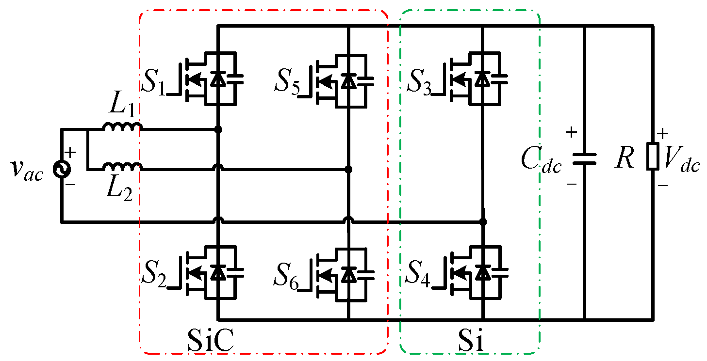
Variable-Frequency Control for Totem-Pole Bridgeless Power Factor Correction Converter to Achieve Zero-Voltage Switching Without Zero-Crossing Detection Circuits

School of Automation, Central South University, Changsha 410083, China
*
Author to whom correspondence should be addressed.
Electronics 2024, 13(16), 3108; https://doi.org/10.3390/electronics13163108 (registering DOI)
Submission received: 30 June 2024 / Revised: 28 July 2024 / Accepted: 2 August 2024 / Published: 6 August 2024

Abstract

:
The totem-pole bridgeless power factor correction (PFC) converter, known for its advantages including simple topology, capability for zero-voltage switching (ZVS), and low common mode interference, presents an opportunity to enhance the efficiency and environmental friendliness of power systems. However, these converters have issues such as ZVS, requiring zero-crossing detection (ZCD) under circuits’ critical continuous mode (CRM) or additional auxiliary resonant circuits, resulting in increased circuit costs and control complexity. Therefore, this paper proposes a variable switching frequency digital control method to achieve ZVS under a wide operating range without ZCD circuits. At the same time, under the premise of ZVS, an interleaved parallel scheme is adopted to further minimize the current ripple and enhance the quality of the current waveform. Finally, an experimental 2 kW two-phase interleaved totem-pole bridgeless PFC converter prototype is designed to verify that the proposed method is correct and effective. The experimental prototype can reach an efficiency of 97.78%.

1. Introduction

A high power factor (PF) and low total harmonic distortion (THD) can save energy and reduce interference with other electronic devices [1,2,3]. Consequently, power factor correction (PFC) converters are beneficial in power supplies to meet the required power quality standards [4,5]. Figure 1 shows the topology of the bridge boost PFC [6,7], where the rectifier bridge shapes the input voltage into a forward full wave while passing through a classic boost converter to obtain the DC voltage. To achieve power factor correction, sinusoidal pulse width modulation (PWM) is used to synchronize the inductance current with the input voltage. Regardless of whether the power transistor is turned on or off, the current will flow through two slow recovery diodes, so the conduction loss of the bridge PFC is higher, especially at low-voltage input applications [8,9,10].
A great deal of research has been conducted on various bridgeless PFC converters to reduce the conduction losses of bridge diodes [11,12]. The totem-pole bridgeless PFC has a simple structure [13], as shown in Figure 2. It has the advantages of low common mode interference, low conduction loss, and the ability to achieve zero-voltage switching (ZVS) of switches in critical continuous mode (CRM). Therefore, it has been widely applied in power supplies, energy storage systems, telecom infrastructure, electric vehicle battery chargers, etc. [14,15]. Meanwhile, with the development and application of wide-bandgap devices, the totem-pole bridgeless PFC has received significant attention due to the possibility of achieving ZVS for switches operated at high switching frequencies.
To further reduce the conduction loss of the totem-pole bridgeless PFC converter, the two diodes in Figure 2 can be replaced with active switches, as shown in Figure 3. Meanwhile, by adopting proper PWM logic, it can also achieve bidirectional power transfer, which is a solution suited to applications that require battery charging/discharging.
As shown in Figure 3, the totem-pole bridgeless PFC converters feature a simple structure, low component counts, and bidirectional power flow capability, attracting widespread attention [15]. With the development of switches, especially wide-bandgap switches, increasing the switching frequency can help to increase the power density of the system and reduce the size of passive components. However, increasing the switching frequency can lead to dominant switching loss due to the influence of various parasitic parameters of the switches. Likewise, research has been conducted on achieving soft switching in totem-pole bridgeless PFC circuits. The application of this technology can reduce the switching loss generated by the switches during high-frequency operation [16]. It is common to achieve ZVS by operating in CRM [16,17,18,19] or by adding additional auxiliary circuits [20,21,22,23]. Compared to adding auxiliary circuits, operating in CRM requires less auxiliary hardware and does not modify the main electrical circuit. In the CRM operation of totem-pole boost converters, zero-current detection (ZCD) circuits are typically incorporated to detect inductor current zero crossings and minimize switching loss [16,17,18,19]. In [16], optimal switching frequency variation range control is employed to optimize the switching frequency range, where the generation of the ZCD signal involves comparing the current sensing signal with a zero reference point. In [17], auxiliary winding is added to assist in obtaining a ZCD signal, and a simple analog-based accurate variable on-time control is proposed to achieve full-load ZVS and power factor correction. In [18], the body diode conduction of the active switch is detected to adjust the synchronous rectification turn-off time to achieve ZVS with minimum turn-on current and reduce the circulating current. However, several challenges arise for these methods relying on ZCD circuits, particularly at high switch frequencies. These include the inaccurate detection of zero-crossing points due to susceptibility to noise from high dv/dt and di/dt operations and the need for additional detecting circuits and PWM logic generation units [18,19].
On the other hand, auxiliary circuits can be added to achieve ZVS without using ZCD circuits. The authors in [20] propose the use of surge-current-limiting circuits to achieve soft switching of a totem-pole bridgeless PFC converter. Additionally, the authors in [21] combine interleaved totem-pole bridgeless PFC with a post-stage dual-active-bridge converter to form a single-stage structure, achieving partial ZVS. In [22], another switch bridge leg and an auxiliary inductor are used in a totem-pole bridgeless PFC rectifier to achieve ZVS of the main switches. In [23], an auxiliary soft-switching cell composed of two inductors, a capacitor, and an FET is added to achieve ZVS. Nevertheless, for these approaches without ZCD circuits, an additional circuit is added to the main circuit, which can increase the converter components and even complicate the working modes, thereby increasing the control complexity.
Consequently, aiming at ZVS over a wide range without the need for ZCD circuits or other additional components, this paper introduces a digital control strategy with variable-frequency control. This strategy incorporates an additional conduction time compensation mechanism that, by dynamically adjusting the switching frequency, allows the current to build up sufficiently before the corresponding switch is turned on. This effectively discharges the switch junction capacitor and allows ZVS to be implemented. This approach not only eliminates the complexity of ZCD circuits but also enhances the performance and reliability of the converter. In addition, the proposed control strategy is adopted in a two-phase interleaved parallel structure to further reduce the current ripple.
This paper is organized as follows: In Section 2, the ZVS models are analyzed with the consideration of switch junction capacitors. The derivation of the conditions and range are of ZVS given in detail. The variable-frequency control method without ZCD circuits and the increased conduction time are analyzed in Section 3. Subsequently, the totem-pole bridgeless PFC converter with two-phase interleaved connections with the proposed control method is analyzed in Section 4. Section 5 presents the experimental results from a 2000 W prototype that verifies the theoretical analysis and proposed modulation schemes. Finally, Section 6 presents the conclusion.

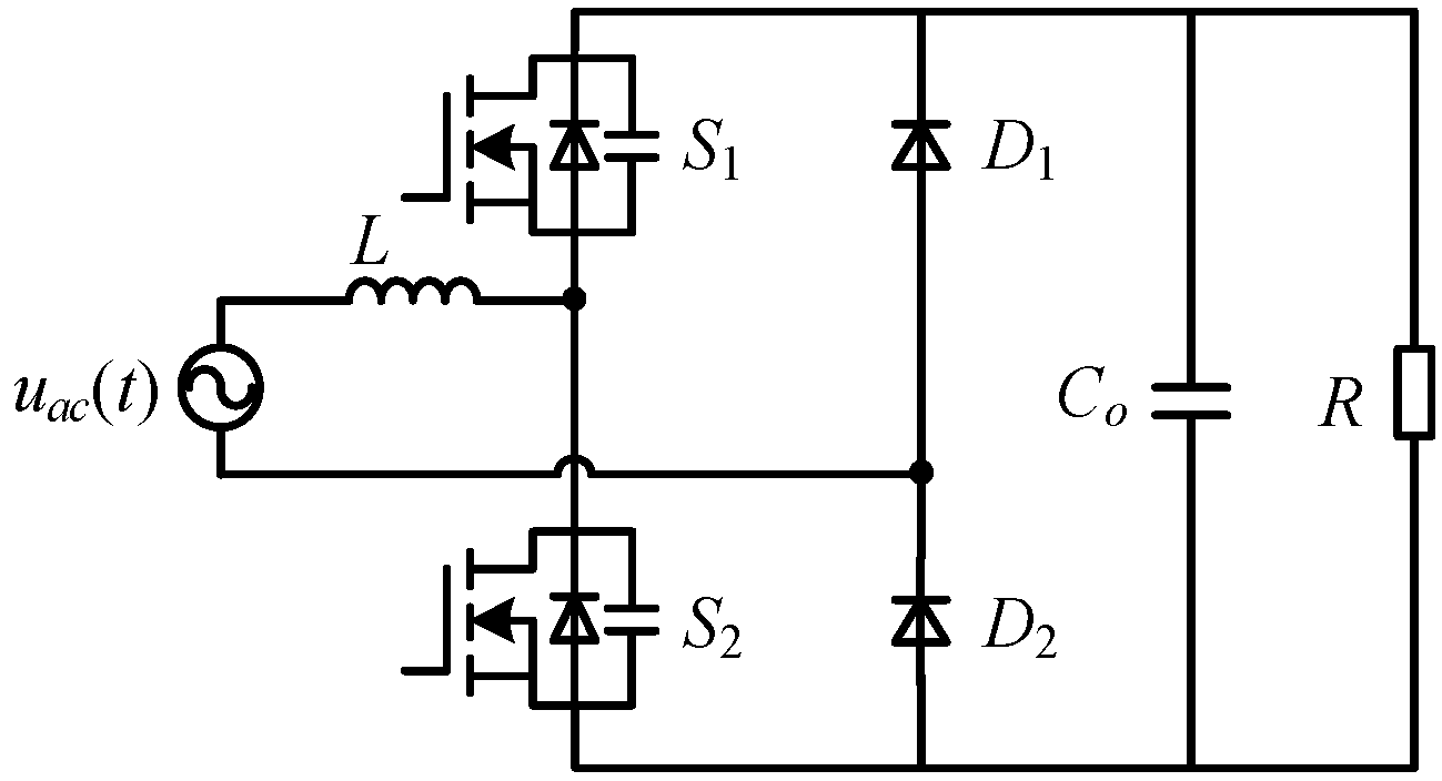
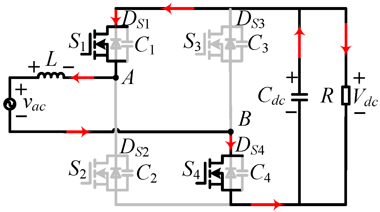
2. ZVS Analysis Considering Switch Junction Capacitors

Achieving ZVS not only reduces switching loss but also EMI noise. This section establishes ZVS models considering switch junction capacitances, derives the necessary ZVS conditions, and defines the ZVS range. This fundamental analysis is employed for the development of a control method to achieve efficient ZVS.

2.1. ZVS Model Analysis with Junction Capacitors

The diodes in the totem-pole bridgeless PFC, as illustrated in Figure 2, are replaced with two Si MOSFETs (S3 and S4), as shown in Figure 4. Combined with corresponding PWM logic, the converter operates in CRM to achieve soft switching. To further reduce switching losses at high frequency, SiC MOSFETs can be used for S1 and S2.
Due to the similar working mode of the SiC totem-pole bridgeless PFC converter in the positive and negative half cycles of AC voltage input, the analysis conducted here is based only on the input voltage in the positive half cycle. The main waveforms of the totem-pole bridgeless PFC rectifier operating in CRM are shown in Figure 5 and can be divided into six stages. vgs1 and vgs2 are the drive signals of S2 and S1, respectively. vS2 is the drain–source voltage of S2. iS1 and iS2 are the currents of S1 and S2, respectively. During the positive half cycle, S4 stays on, S3 stays off, and S2 and S1 are the main switches operating with high switching frequency.
Stage 1 [t0t1] is shown in Figure 6a. At t0, S2 is turned off, and the inductor current iL charges the junction capacitor C2 of S2 while discharging the junction capacitor C1 of S1. The duration of stage l is relatively short since iL is at its peak at t0 and thus the charging process will be over in a short time. At t1, S1 is turned on. After this stage, the current that previously flowed through S2 continues to flow through S1. The voltage vc2 of C2 can be expressed as
v c 2 ( t ) = i L ( t 0 ) t / ( 2 C o s s )
where Coss is the junction capacitor of S1 and S2, with Coss = C1 = C2.
Stage 2 [t1t2] is shown in Figure 6b. In this stage, at t1, the voltage vds2 of S2 increases to the bus voltage Vdc. Meanwhile, the voltage vds1 of S1 decreases to 0, and the diode DS1 of S1 conducts. S1 achieves ZVS, and the voltage of L is equal to Vdcvac(t). The inductor current iL linearly decreases, and iL decreases to 0 at t2. In this stage, the inductor current iL can be expressed as
i L ( t ) = i L ( t 1 ) ( V d c v a c ( t ) ) t / L
Stage 3 [t2t3] is shown in Figure 6c. At t2, S1 is turned off, and the diode DS1 of S1 continues to conduct due to reverse recovery. Moreover, iL is reversed and continues to decrease, and can be expressed as
i L ( t ) = ( V d c v a c ( t ) ) t / L
Stage 4 [t3t4] is shown in Figure 6d. At t3, the diode DS1 of S1 is cut off, and C1, C2, and L begin to resonate. The voltage vds2 of S2 begins to decrease, and the drain–source voltage vds1 of S1 begins to rise. vds2 decreases to the minimum value at t4, and this stage ends. During this stage, the relationship can be shown as
i L ( t ) = ( V d c v a c ( t ) ) sin ω 0 t / Z + i L ( t 3 ) cos ω 0 t
And the drain–source voltage of S2 can be expressed as
v d s 2 ( t ) = v a c ( t ) + ( V d c v a c ( t ) ) cos ω 0 t + i L ( t 3 ) Z sin ω 0 t
Here, Z = L / 2 C o s s , ω 0 = 1 / 2 C o s s L .
Stage 5 [t4t5] is shown in Figure 6e. At t = t4, the drain–source voltage of S2 decreases to zero, and the diode DS2 of S2 conducts. During this stage, iL rises from a negative state to 0, which can be expressed as
i L ( t ) = i L ( t 4 ) + v a c ( t ) t / L
Stage 6 [t5t6] is shown in Figure 6f. At t5, S2 is turned on by the gate drive signal. If Vds2 is zero, the turn-on of ZVS will be achieved. Subsequently, iL increases linearly until t = t6, and S2 turns off and repeatedly enters the next cycle. The expression for iL is
i L ( t ) = v a c ( t ) ( t t 5 ) / L

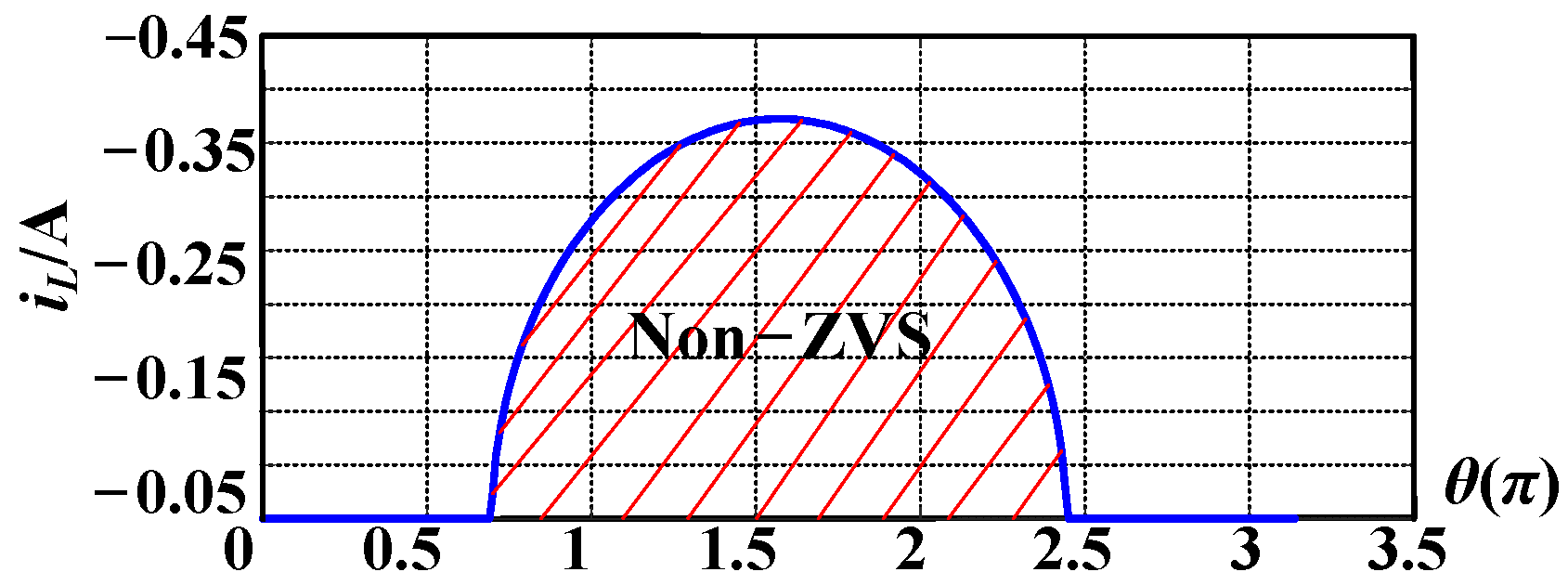
2.2. ZVS Condition and Region

In stage 4, the totem-pole bridgeless PFC achieves turn-on of the ZVS or valley through the resonance between the inductor current and the junction capacitor of the high-frequency switch. In the traditional CRM, from (5), if IL(t3) = 0, the valley value of the voltage vc2 of C2 is deduced as vc2 = 2vac(t) − Vdc and the voltage vc1 of C1 is vc1 = vdcvc2(t) = 2vdc − 2vac(t). Therefore, the condition for achieving ZVS in S2 is
v c 2 ( t ) = 2 v a c ( t ) V d c 0 v a c ( t ) V d c / 2
Thus, when the input voltage vacvdc/2 during its positive half cycle, S2 can achieve ZVS turn-on. However, it cannot when vac > vdc/2. Under this condition, C2 needs to be discharged with an additional charge current or energy. The additional charge Qe needs to meet the following:
Q e C s 2 ( 2 v a c ( t ) V d c ) + C s 1 ( V d c ( 2 V d c 2 v a c ( t ) ) ) = 2 C o s s ( 2 v a c ( t ) V d c )
After normalization, Qe* can be obtained:
Q e * Q e / ( 2 C o s s V o ) 2 v i n ( t ) / V o 1 = 2 k 1
where k = vac(t)/Vdc and Qe* is proportional to k.
Equations (9) and (10) yield the ZVS region, which is also shown in Figure 7, illustrating the Qe* charge required to achieve ZVS across different instant input voltages, where k is the voltage conversion gain. The graph reveals two regions: the “A-Natural ZVS” region, where ZVS can be achieved without extra charge energy under the case k ≤ 0.5, and the “B-ZVS Expansion” region, denoting ZVS performance under k > 0.5. Notably, for k > 0.5, the inductor current must cross zero to provide an extra charge Qe* to achieve ZVS. Consequently, in CRM, the charge energy becomes ineffective under k > 0.5 when the inductor current stays at zero, resulting in the absence of soft switching, as observed in traditional CRM.
In real applications, Qe* can be generated by adding extended conduction time for the active power switches. However, this extension must be implemented after the zero-crossing point of the inductor current. In conventional control strategies dependent on ZCD, it is insufficient to merely detect the zero-crossing point. The system needs to compensate for the delay and guarantee adequate negative current for the achievement of ZVS. This requires complex calculations and compensations based on the power conditions and the precise timing of the zero-crossing event.

3. Variable-Frequency Control without ZCD Circuits to Achieve ZVS Considering Switch Junction Capacitors

In this section, an eliminating ZCD circuit control method with variable frequency is proposed to achieve the full-range ZVS of totem-pole bridgeless PFC. The circuit model is established with consideration of the switch junction capacitors. Based on this model, the minimum charging current of the inductor is derived, and thus, the additional compensated turn-on time for the switches is obtained. Further, the control to extend the turn-on time is combined with the variable-frequency control in the DSP implementation.

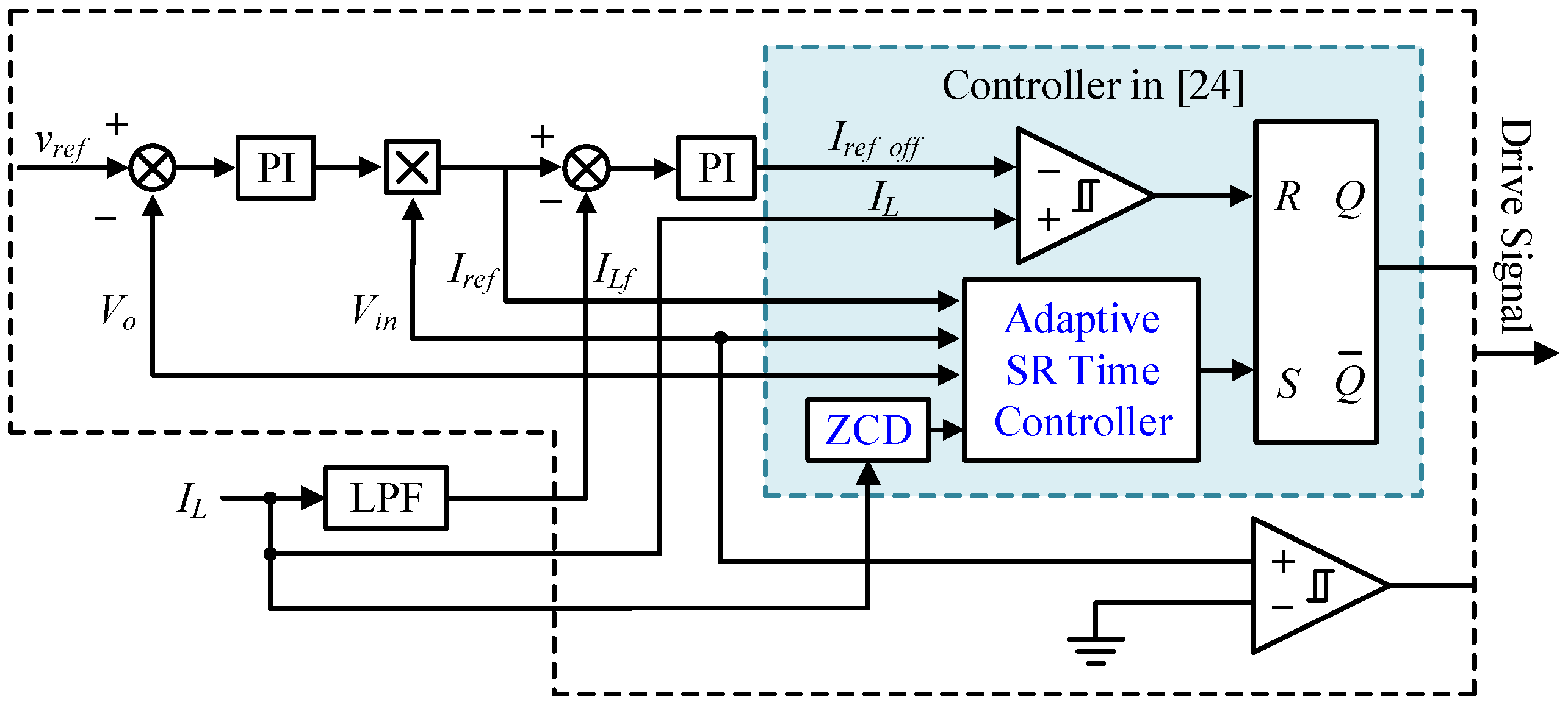
3.1. Conventional Method with ZCD and the Concept Diagram without ZCD

The conventional methods for achieving ZVS typically rely on ZCD circuits, as exemplified in [24]. The corresponding control block diagram is illustrated in Figure 8. As shown, a double loop control is adopted to generate the peak current reference for the hysteresis comparator to compare with the inductor current iL to control the peak value of the inductor. Meanwhile, a ZCD unit is adopted to control the valley point of iL. It should be noted that the energy is not sufficienct to discharge the junction capacitor of the switches if the turn-off current is strictly equal to zero, as discussed in Section 2.2. Thus, an adaptive SR time controller is needed to slightly adjust the turn-off time instant. This involves intricate calculations and compensations based on the power conditions and the precise timing of the zero-crossing event. Consequently, the control strategies with ZCD circuits still involve complexity, especially at high switching frequencies utilizing SiC MOSFETs, where accurate timing is critical and delay or noises can affect performance.
Actually, to achieve ZVS for the switches of totem-pole bridgeless PFC converters, the key concept is to ensure that the switch turn-off current stays near zero (the energy is not sufficient to discharge the junction capacitor of the switches if the turn-off current is strictly equal to zero). Essentially, the inductor current value is related to the switching frequency, duty cycle, input voltage, output voltage, etc. So, the desired switch turn-off instant current can be controlled by controlling the switching frequency. Consequently, a concept diagram of the proposed control is shown in Figure 9. As can be seen, a variable frequency control unit is adopted rather than using a ZCD and adaptive SR time controller in Figure 8. Similar to conventional digital control of PFC, the voltage and current loops generate the signal for the PWM unit, and the modulation frequency is controlled through a variable frequency unit (the detailed derivation for the variable frequency will be analyzed in Section 3.2). This direct variable frequency control can respond more precisely, avoiding the possible delay and complexity brought by the ZCD circuit.

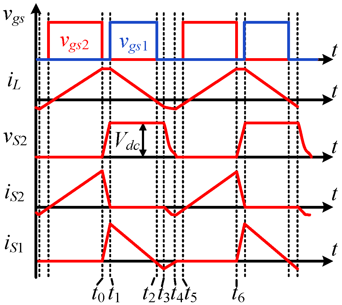
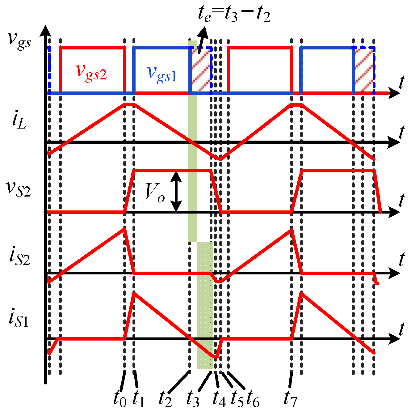
3.2. Working Principal Analysis and Variable Frequency Derivation without ZCD to Achieve ZVS

As in a previous discussion, the variable frequency unit is the key controller for the proposed concept. Thus, based on the working principal analysis, illustrating the relationship between the switch turn-off current and the switching frequency and then deriving the frequency control law to achieve ZVS are important. It is also important to investigate how real-time adjustments to the switching frequency function and ensure ZVS without relying on ZCD for zero-crossing detection.
Figure 10 illustrates the operational waveforms of the converter in CRM during the positive half cycle of the AC voltage. During the period in which S2 is turned on and S1 is turned off, the voltage across the inductor L is fixed, causing a linear rise in iL. Concurrently, the input voltage vac(t) during this interval is expressed as
v a c ( t ) = V m sin ( ω t ) = L i p k ( t ) / T o n ( t )
Here, for S1, Ton is the turn-on time. Subsequently, iL linearly decreases when S1 is turned on, and vac(t) is calculated as
v a c ( t ) = V m sin ( ω t ) = L i p k ( t ) / T o f f ( t ) + V d c
Here, Toff denotes the turn-off time.
With CRM, the envelope of the peak value of iL(t) is denoted as ipk(t) = 2iavg(t). Moreover, throughout a half cycle, iavg(t) equals the AC current. Therefore, the expression for the peak value of iL(t) is obtained as
i p k ( t ) = 2 I m sin ( ω t )
Furthermore, the Ton and Toff of the SiC switches can be determined by applying the volt-second area balance principle of the inductor.
T o n ( t ) = L i p k ( t ) / v a c ( t ) = 2 L i a v g ( t ) / v a c ( t )
T o f f ( t ) = L i p k ( t ) / ( V d c v a c ( t ) ) = 2 L i a v g ( t ) / ( V d c v a c ( t ) )
Combining (13)–(15), the frequency condition to achieve CRM operation can be derived.
f s ( t ) = 1 / ( T o n ( t ) + T o f f ( t ) ) = v a c ( t ) ( V d c v a c ( t ) ) / ( 2 L i a v g ( t ) V d c )
Equation (16) represents the frequency expression in CRM. In digital control, the frequency can be used to update the cycle count value in DSP. Based on (16), the variation trend of fs within half a cycle is plotted as an example case in Figure 11. As shown, fs is the lowest at π/2, which is the peak/valley value of the input sine voltage. When vac(t) approaches zero, the switching frequency is the highest.
The previous analysis in Section 2.2 shows that in the CRM operation, the totem-pole bridgeless PFC can only naturally achieve ZVS when the input AC voltage is less than half of the output DC voltage.
Figure 12 illustrates the waveform when adding the additional conduction time within the descending phase of the inductor current, where te = t3t2 represents the additional conduction time. Because the two stages of [t0t1] and [t1t2] are the same as the traditional CRM control, which has been analyzed in Section 2.1, they will not be discussed here. Compared to the mode analysis in Section 2.1, an additional mode has been added, which is the additional conduction mode from t2 to t3, as shown in Figure 13. The specific analysis for modes from t2t6 is discussed as follows.
Stage 1 [t2t3]: At t2, the inductor current iL crosses 0, and the driving signal for S1 continues to conduct instead of turning off, causing iL to reverse and continue to decrease. The expression of iL in this mode is the same as (3). At t3, iL decreases to the bias current (or valley point) iLzvs to provide energy to charge the switch junction capacitors. The bias current is used to charge and discharge the junction capacitor of the high-frequency switches, which can be expressed as
i L z v s ( t ) = ( V d c v a c ( t ) ) ( t 3 t 2 ) / L
Stage 2 [t3t4]: At t3, S1 is turned off, and the body diode of S1 undergoes reverse recovery. iL continues to decrease in reverse, and the duration of this stage is very short.
Stage 3 [t4t5]: At t4, the body diode of S1 is cut off, and L, C1, and C2 begin to oscillate. At t5, the voltage of S2 drops to 0.
Stage 4 [t5t6]: During this mode, the body diode of S2 is on, and L is charged through S2. When t = t5, iL is reversed. At this stage, the drain–source voltage of S2 continues to be 0, which means S2 can achieve ZVS.
Based on the above analysis, the additional conduction time of S3 and S4 can be controlled to reverse the charge and store energy for the inductor current, which can be used for the energy charging of the junction capacitor of the switches in the high-frequency bridge arm to achieve ZVS. The analysis of the negative bias current required for the inductor current to achieve ZVS is as follows:
In the resonance stage of inductor L and capacitors C1 and C2 (refer to Figure 6 d for the circuit stage), the following formula can be obtained based on the relationship between capacitor current and inductor voltage:
C 1 d v c 1 d t = i L + C 2 d v c 2 d t
L d i L d t + v a c V d c + v c 1 = 0
v c 1 = V d c v c 2
Taking C1 = C2 = Coss and substituting (20) into (18), the following is deduced:
C o s s d v c 1 d t = i L + C o s s d ( V d c v c 1 ) d t = i L C o s s d v c 1 d t 2 C o s s d v c 1 d t = i L
Based on (1) and (21), the equivalent circuit displayed in Figure 14 can be illustrated.
From the above equivalent circuit, based on energy conservation, (22) can be obtained, where iLzvs is the bias current to achieve the turn-on of ZVS in the main switch.
0.5 L i L z v s 2 ( v a c V d c ) i L d t + 0.5 2 C 1 v c 1 2
Substituting (21) into (22) yields the iLzvs conditions that need to be met to achieve the main switch ZVS.
i L z v s ( t ) 2 [ 2 C o s s V d c ( v a c ( t ) V ) ( v a c ( t ) V d c ) ] / L + C o s s V d c 2
Therefore, by substituting the relevant circuit parameters into (23), the bias current required for the main switch to achieve ZVS can be plotted as an example to show the inductor current required to achieve ZVS under different instant input voltages, as shown in Figure 15. As shown, when the grid voltage is relatively low, ZVS can be achieved without the need for additional negative current. When the grid voltage is higher, the switches need an additional negative bias current to achieve ZVS.
Consequently, through substitution of the required inductor current into (16), the frequency condition to achieve full-working-range ZVS can be calculated as
f s _ f u l l ( t ) = v a c ( t ) ( V d c v a c ( t ) ) / [ 2 L ( i a v g ( t ) + i L z v s ( t ) ) V d c ]

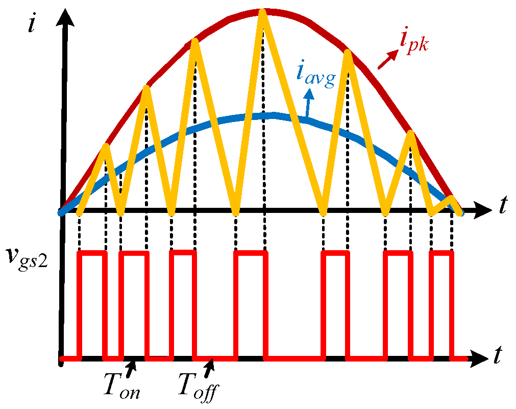
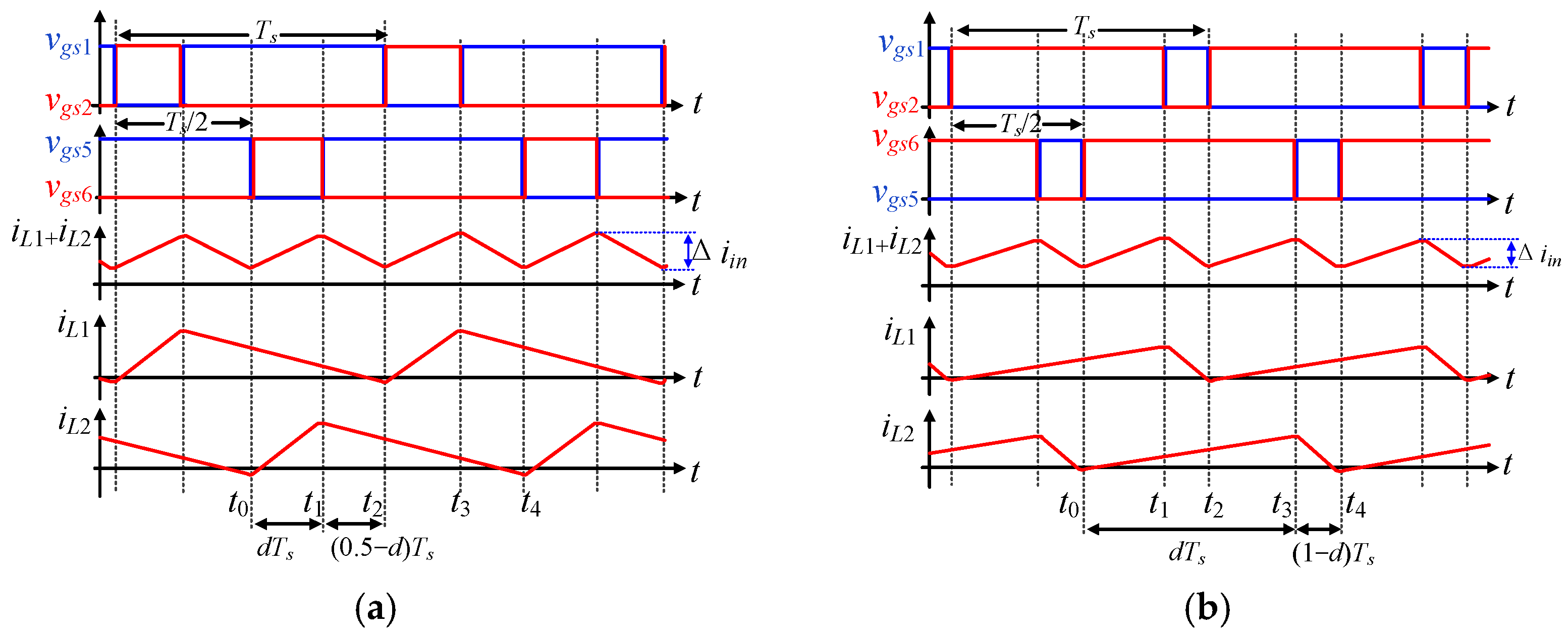
4. Current Ripple Reduction and Digital Implementation of the Proposed Control Method

As previously mentioned, achieving ZVS in CRM reduces switching turn-on losses, but the peak-to-peak inductor current, nearly double the average current, can increase high-frequency ripple at the AC input. To mitigate this issue, the proposed control method can be applied to a totem-pole bridgeless PFC converter with two-phase interleaved connections [25]. This section provides current ripple models to demonstrate the effectiveness of the interleaved structure and analyzes how the proposed control method is implemented in this configuration.

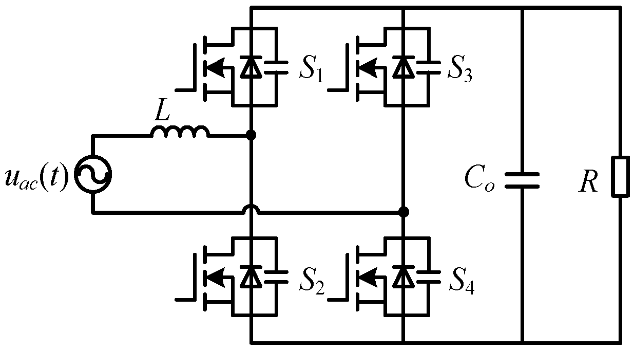
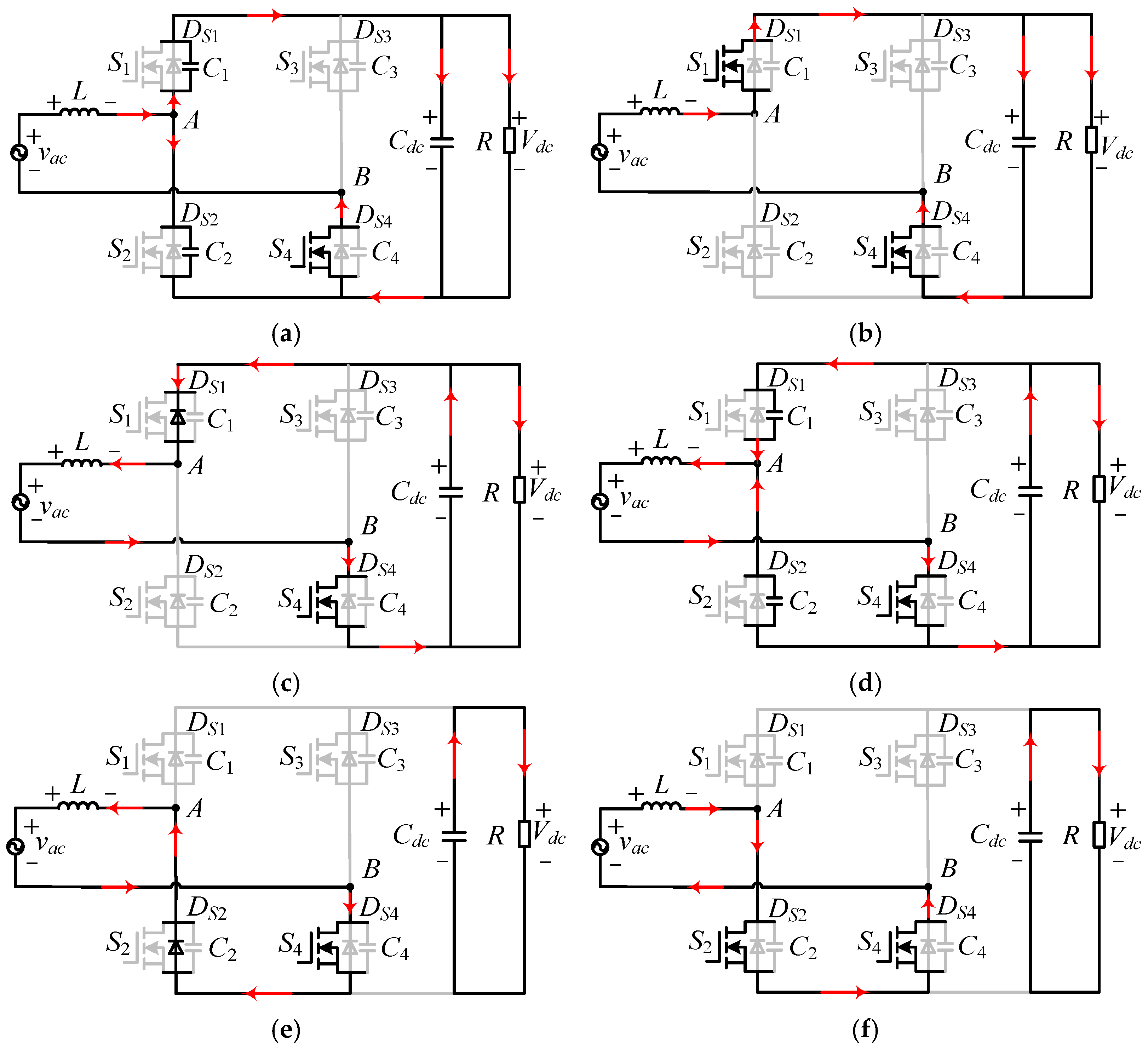
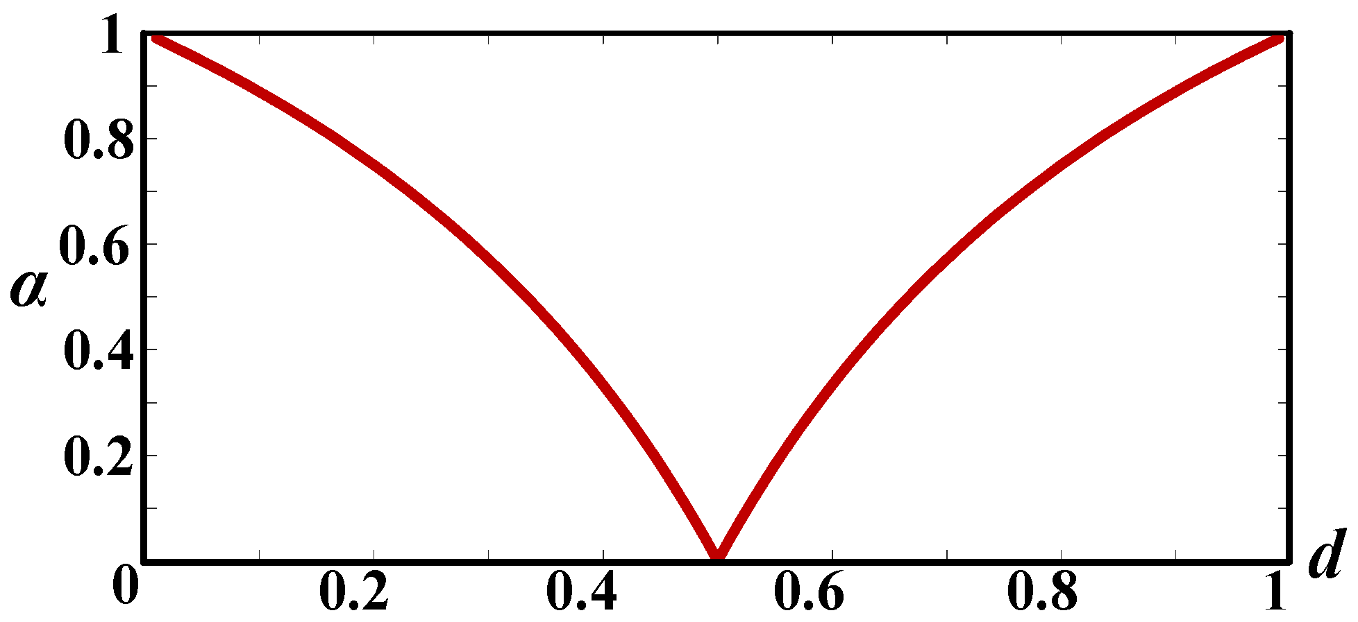
4.1. Current Ripple Reduction with Two-Phase Interleaving for Totem-Pole Bridgeless PFC Converter

Two-phase interleaving refers to adding a set of high-frequency bridge arms and inductors to the original single-phase totem-pole bridgeless PFC topology and multiplexing the power frequency bridge arms for parallel connection. It is worth noting that each phase in an interleaved structure can be regarded as operating independently. The interleaving structure does not alter the fundamental working principle of each phase. The topology is shown in Figure 16. High-frequency switches S1 and S2 and inductor L1 form the main phase; high-frequency switches S5 and S6 and inductor L2 form the secondary phase; and S3 and S4 are multiplexed as the main and secondary phases.

4.2. Analysis of Current Ripple Reduction with Two-Phase Interleaving

The duty cycles d of the two main switches S2 and S6 are the same, while the driving phase for them is 180° phase-shifted, causing the inductor current of the main and secondary phases to differ in phase by 180°. The synchronous rectifiers S1 and S5 complement the main switches S2 and S6 in conduction. Due to the on-and-off states of S2 and S6, the converter consists of four different stages based on the analysis of the input voltage during the positive half cycle. When the interleaved converter operates in CRM, they have different current waveforms at duty cycles d ≤ 0.5 and d > 0.5. Figure 17a shows the main waveform of the inductor current with d ≤ 0.5, and Figure 17b shows the main waveform of the inductor current with d > 0.5. The following is an analysis of the current ripple under these two cases.
(1)
d ≤ 0.5
From Figure 17a, the inductor currents iL1 and iL2 of the two phases both linearly decrease in the [t1t2] and [t3t4] stages, indicating that the above converter operates in Mode 4. Based on the equivalent circuit of Mode 4, it can be concluded that
{ L 1 Δ i L 1 / Δ t = V d c v a c L 2 Δ i L 2 / Δ t = V d c v a c
At steady state, the expression for the duty cycle d is
d ( t ) = 1 | v a c ( t ) | / V d c
Assuming that the two inductors are the same, there are
{ L 1 = L 2 = L Δ t = ( 1 / 2 d ) T Δ i i n = Δ i L 1 + Δ i L 2
Substituting (26) and (27) into (25), the total input current ripple can be obtained as
Δ i i n = d ( 1 2 d ) v a c / [ ( 1 d ) L f s ]
(2)
d > 0.5
In the stages of [t0t1] and [t2t3], the inductor currents iL1 and iL2 of both phases increase linearly, corresponding to operating Mode 1 of the converter mentioned above. Therefore, according to the corresponding equivalent circuit, it can be obtained as
{ L 1 Δ i L 1 / Δ t = v a c L 2 Δ i L 2 / Δ t = v a c
Similarly, there are
{ L 1 = L 2 = L Δ t = ( d 1 / 2 ) T Δ i i n = Δ i L 1 + Δ i L 2
Substituting (26) and (30) into (29), the total input current ripple can be obtained as
Δ i i n = ( 2 d 1 ) v a c / ( L f s )
Based on the volt–ampere relationship of the inductor current, it can be obtained by combining (28) and (31) that the input current ripple expression of the interleaved converter in CRM can be obtained as
Δ i i n = { d ( 1 2 d ) v a c / [ ( 1 d ) L f s ]       d < 0.5 ( 2 d 1 ) v a c / ( L f s )                                     d 0.5
The ripple current of a single inductor is
L Δ i L / Δ t = v a c Δ i L = v a c Δ t / L = d v a c / ( L f s )
The ratio of the total input current ripple to the current ripple of a single inductor is defined as α = ΔIinIL. Substituting (32) into (33) yields
α = { ( 1 2 d ) / ( 1 d )       d < 0.5 ( 2 d 1 ) / d                             d 0.5
According to (34), the relationship between the current ripple ratio α and the duty cycle d is shown in Figure 18. According to Figure 18, the ripple current is always smaller than the single ripple current (ripple ratio α < 1) after interleaving. And when d is around 0.5, the current ripple after interleaving is canceled. Therefore, adopting the interleaved parallel scheme has advantages in reducing the current ripple of the converter in CRM.

4.3. Digital Implementation of the Proposed Control Method for Two-Phase Interleaved Parallel Totem-Pole Bridgeless PFC

The control methods of interleaving are mainly divided into open-loop interleaving based on the ZCD circuit and closed-loop interleaving based on a phase-locked loop. Open-loop interleaved parallel connection divides each phase circuit into one main phase and multiple secondary phases, where the main phase circuit works independently like a single-phase PFC converter. It can work in current mode or voltage mode, and the driving signals of each secondary phase are obtained based on the driving signals of the main phase after a certain delay. It can be divided into four categories based on the working mode of the circuit and the synchronization time of each phase: voltage mode on-time synchronization, current mode on-time synchronization, current mode off-time synchronization, and voltage mode off-time synchronization. Closed-loop interleaving adjusts the turning-off time of the secondary phase based on phase error, thereby achieving an interleaving parallel connection. The above two methods require a ZCD circuit on both the primary and secondary phases, increasing the complexity of the circuit.
According to the previously discussed variable-frequency control method without the use of ZCD circuits, the proposed digital control strategy for a two-phase interleaved parallel totem-pole bridgeless PFC is illustrated in Figure 19. As illustrated, this integration enables the control method to achieve ZVS without the need for supplementary sensors, auxiliary circuits, or ZCD circuits, thereby enhancing noise immunity and ensuring precise control. The output voltage of the rectifier is sampled as the feedback of the output voltage loop, and the output of the voltage loop is multiplied with the grid phase to generate the reference of the inner current loop, in which the phase of the current is obtained through a digital PLL unit. The frequency calculation unit calculates the on-time frequency based on the equation shown in (24) and updates the timer in the DSP in each switching cycle. The duty cycle of each switch is calculated based on the output of the inner current loop with a feedforward of the AC voltage.

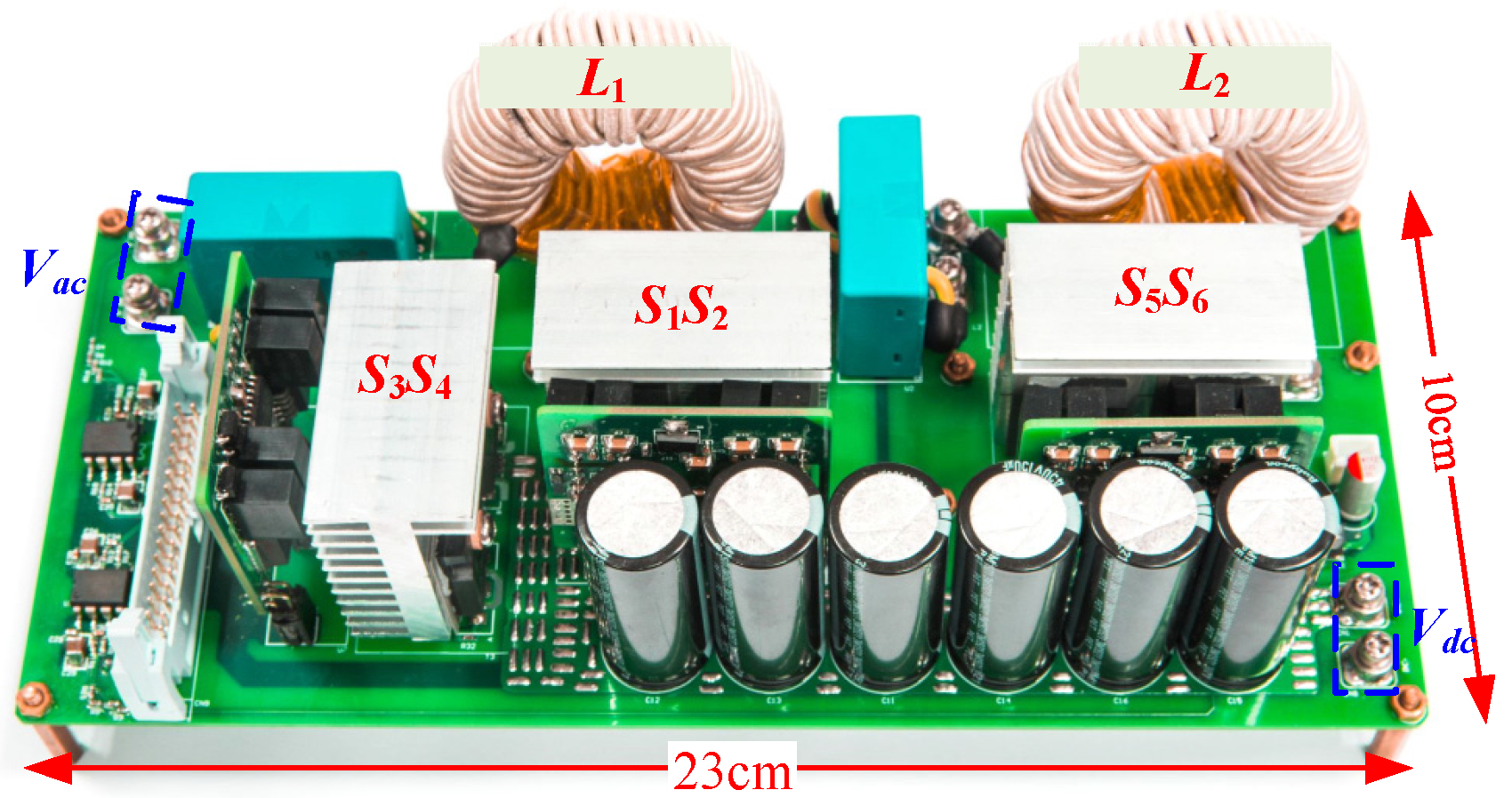
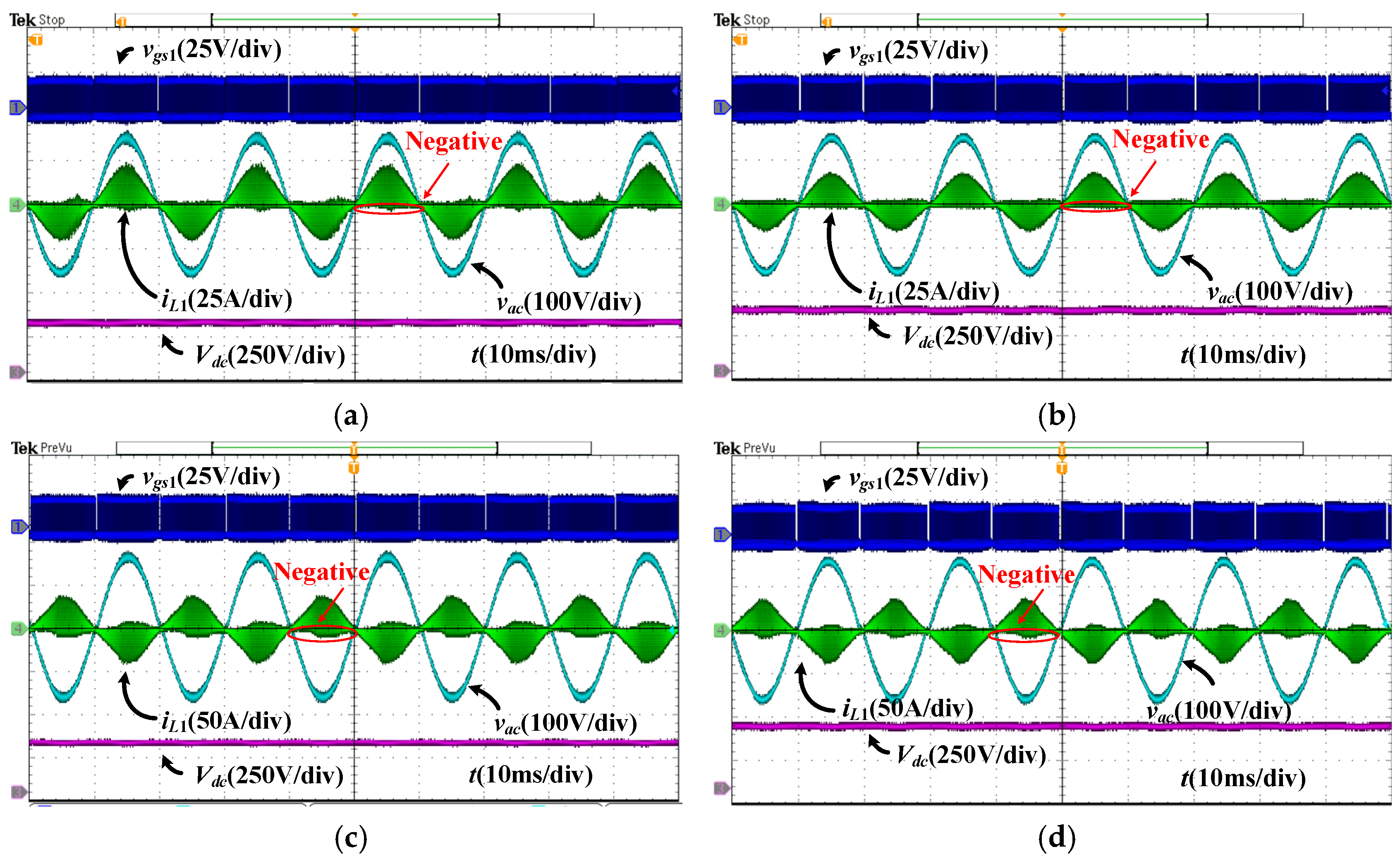
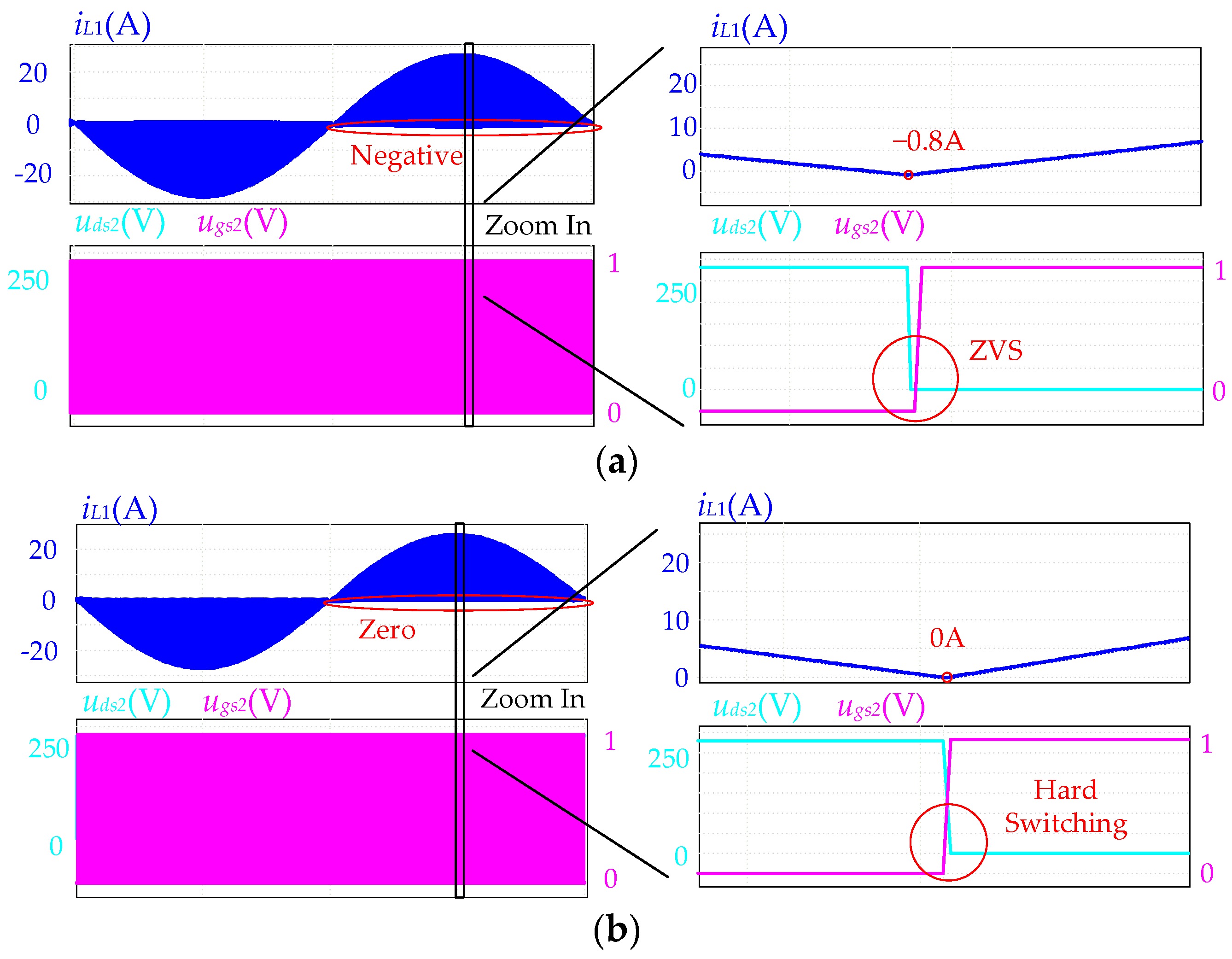
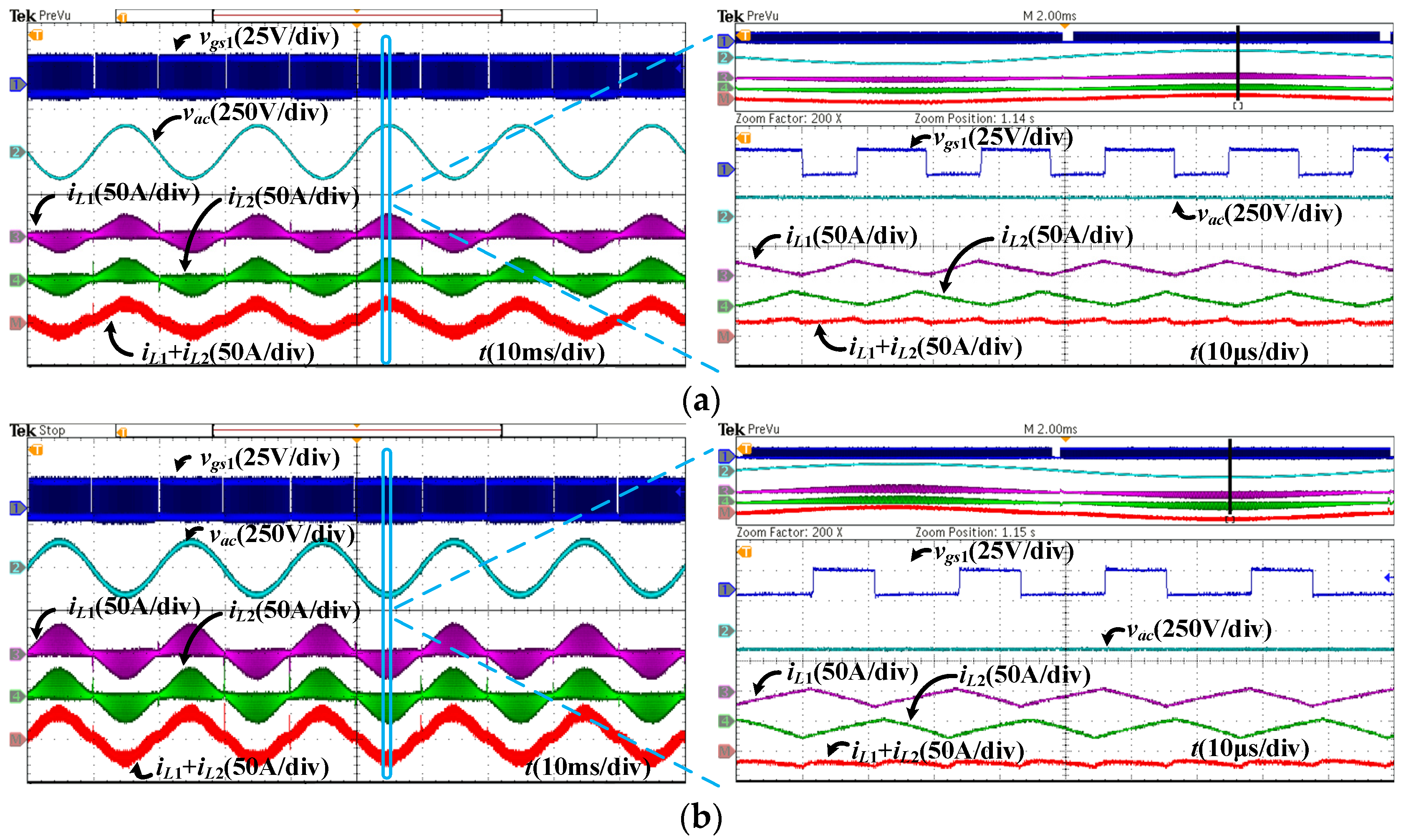
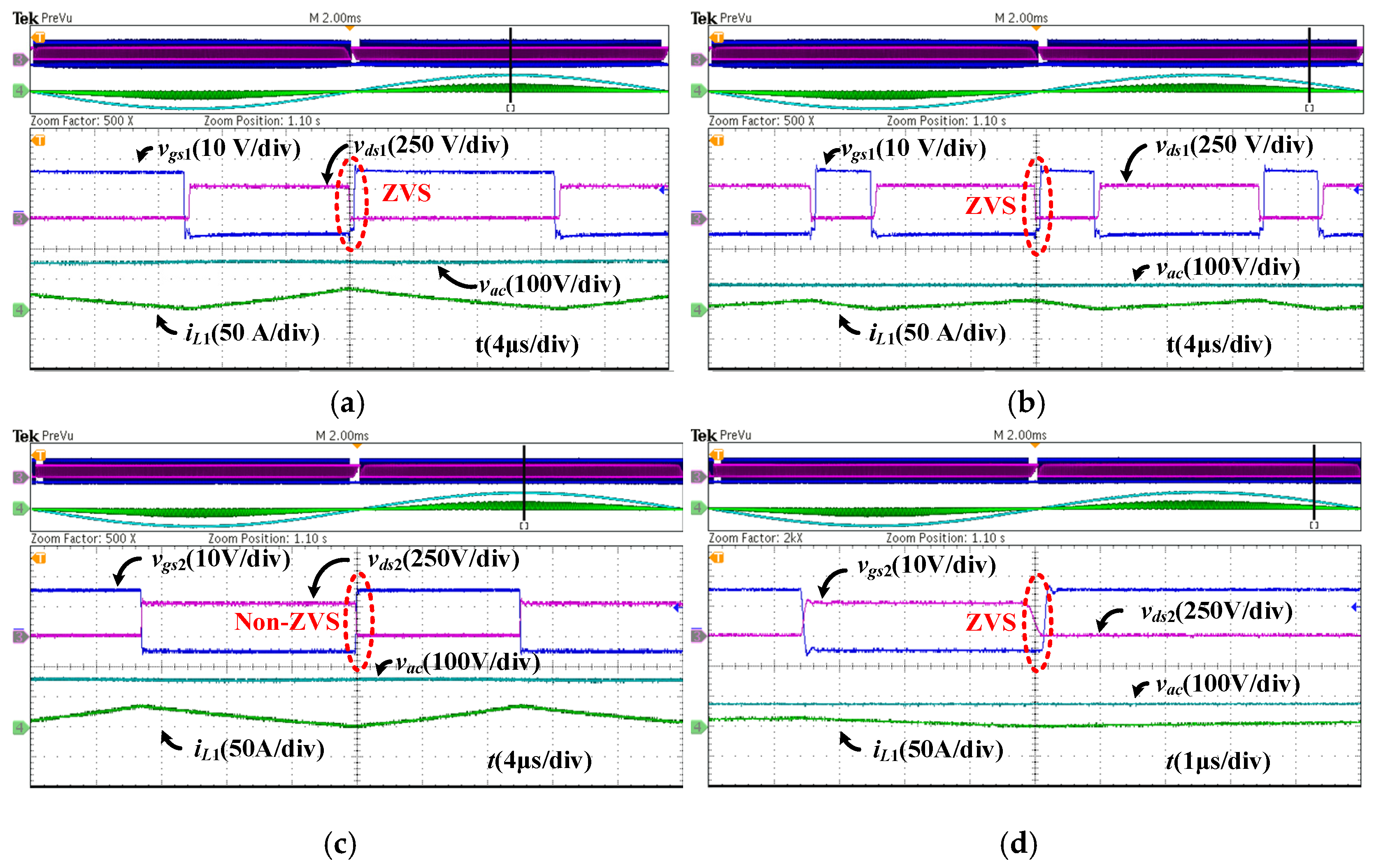
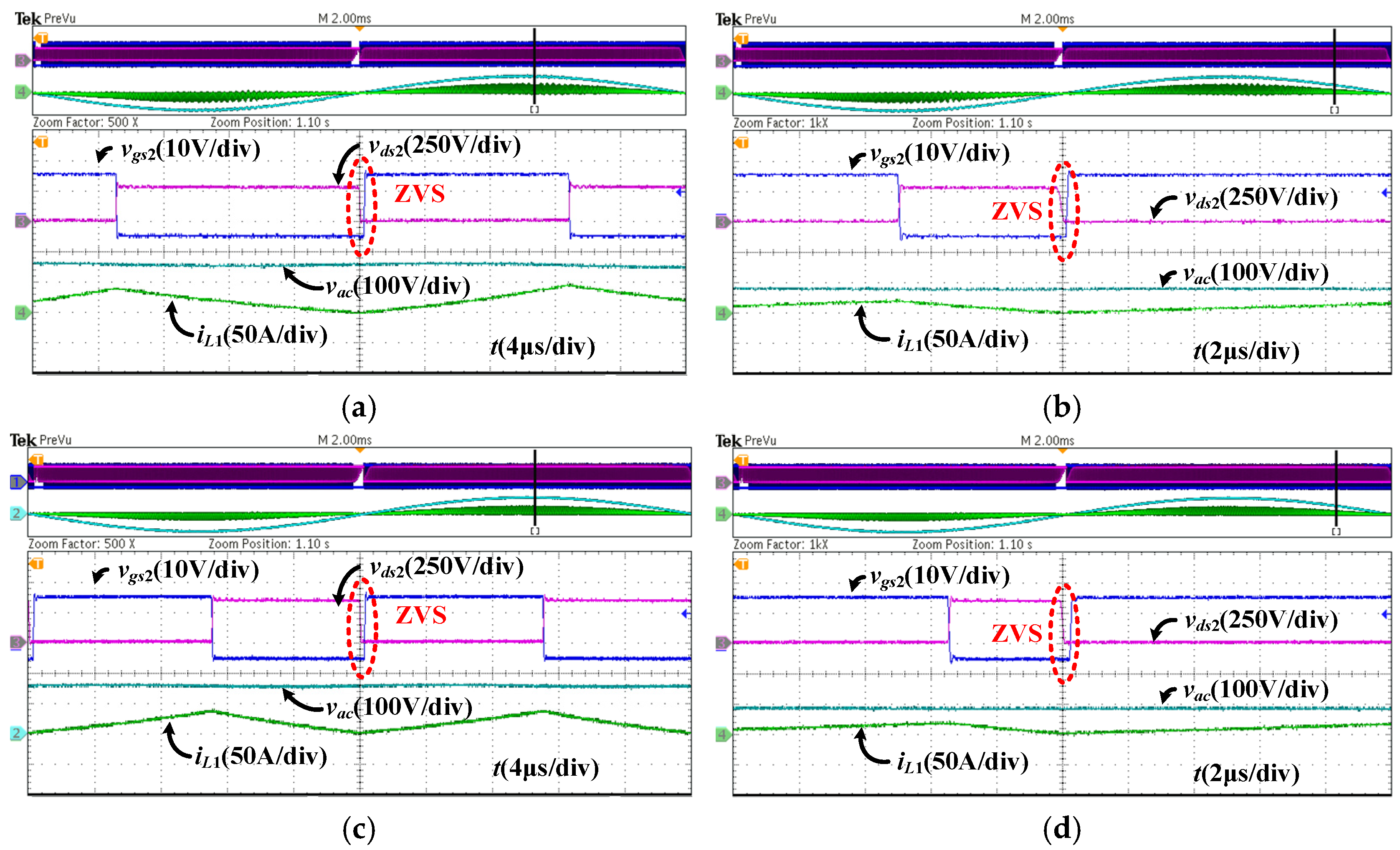
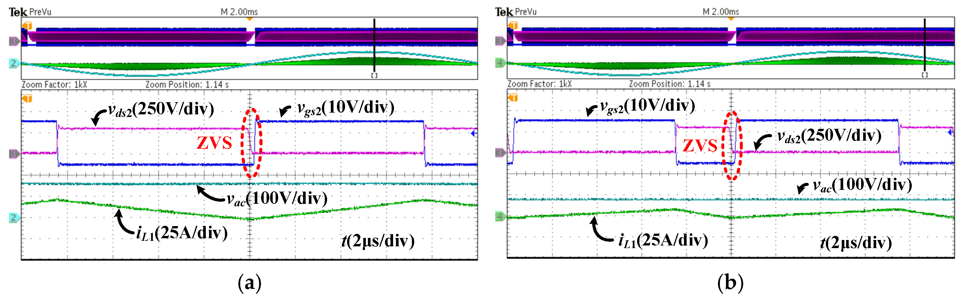
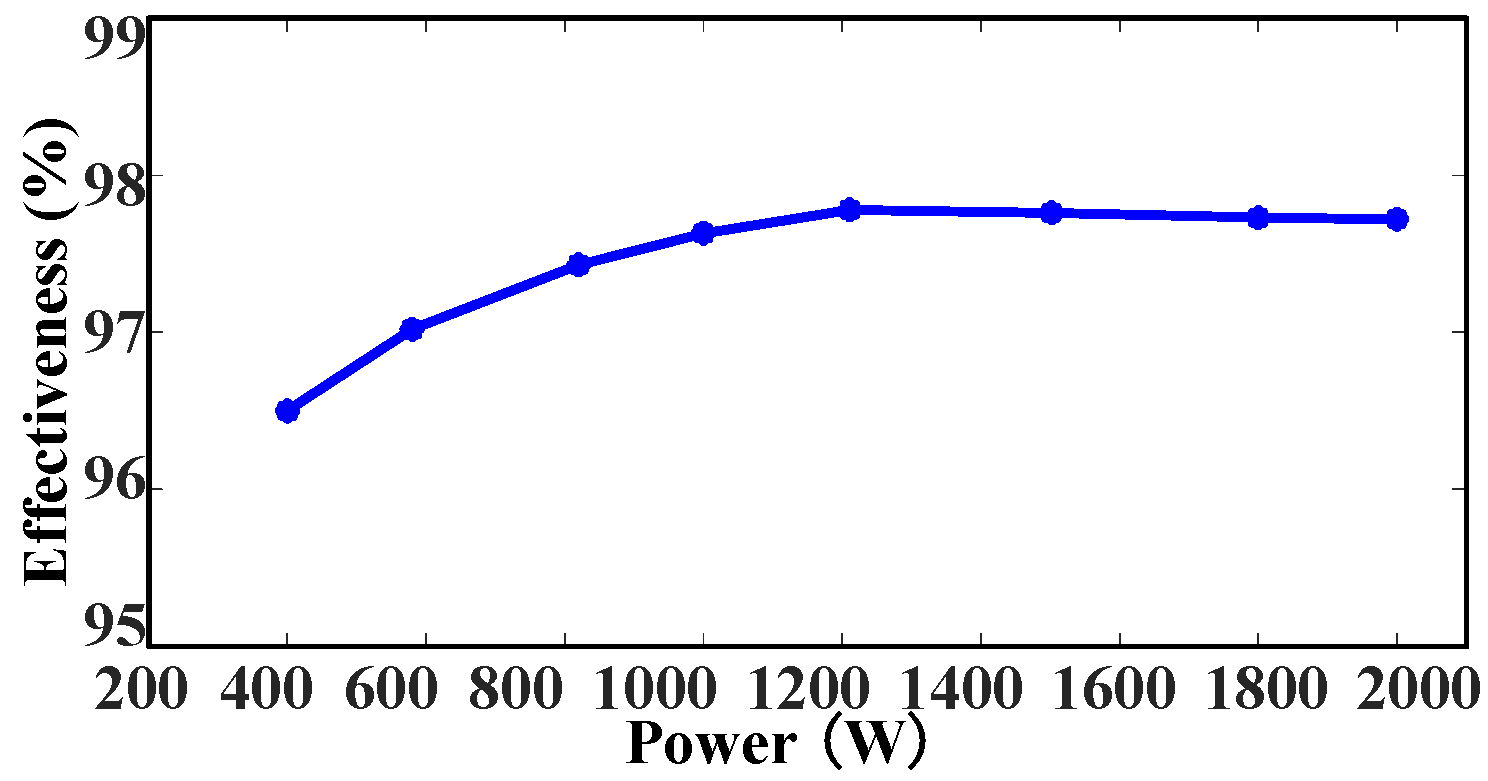
5. Experimental Verification

To validate the effectiveness of the proposed control method for the totem-pole bridgeless PFC converter, a 2000 W experimental prototype was designed for practical verification. The experimental prototype is shown in Figure 20. The main parameters of the experimental prototype are provided in Table 1.
Utilizing the variable-frequency control method, Figure 21 illustrates the forward and reverse power operation waveforms of a single-phase full load (1000 W) under the proposed control method. The output bus voltage on the DC side is 280 V and 370 V in Figure 21a,c and Figure 21b,d, respectively, which show two operation cases for k > 0.5 and k < 0.5. As seen, the inductor current iL1 has a small current bias instead of staying at zero in both positive and negative half cycles for all the waveforms, indicating the effectiveness of the current value control near the zero-crossing point. It can be observed that the inductor current can be negative, which is a crucial characteristic of the additional conduction time.
Comprehensive simulations were conducted to further validate the effectiveness of the proposed variable switching frequency with additional conduction time. As shown in Figure 22a, when the additional conduction time is injected based on (24), the inductor current is negative before S2 turns on. This negative current plays a crucial role in discharging the switch junction capacitor of S2, thereby facilitating the achievement of ZVS. In contrast, as depicted in Figure 22b, when the variable-frequency control is implemented without the additional conduction time based on (16), iL is nearly zero before S2 turns on, resulting in hard switching.
Figure 23 shows the performance of the current ripple reduction adopting the interleaved structure under different load conditions. As can be seen, after interleaving, the current ripple of the sum of the two inductor currents (iL1 + iL2) becomes much smaller compared with the one for each single phase (iL1 or iL2). Additionally, the expanded waveforms for the three currents are also shown, which demonstrate the effectiveness of the current ripple reduction.
Figure 24 shows the ZVS achievement of the two switches S1 and S2 on the single-phase full load (1000 W) in the traditional CRM control method. As seen in Figure 24c, S2 cannot achieve ZVS when k > 0.5, indicating that the ZVS region is limited when the converter only operates in CRM and that ZVS cannot be achieved over a wide voltage range.
Figure 25 shows the ZVS performance in the main switch with a single-phase full load (1000 W) under the proposed variable-frequency control method for the converter at different DC side output voltages. As shown in Figure 25a,c, if the DC bus voltage is greater than the AC voltage and the negative bias current is increased, both at Vdc = 280 V and Vdc = 370 V, when the input voltage is in the positive half cycle, S2 achieves ZVS turn-on. Similarly, within the negative half cycle, S1 can also achieve ZVS. Therefore, it is verified that the variable-frequency control without ZCD circuits proposed in this paper can achieve ZVS in the totem-pole bridgeless PFC converter under different output voltages.
Figure 26 shows the ZVS implementation for the single-phase half load (500 W) output of the converter under the proposed variable-frequency soft-switching control method. As shown in Figure 26a,b, the main switch S2 achieved ZVS at different input voltage values and under different voltage conditions during the positive half cycle.
Figure 27 shows the power loss breakdown under different loads, including half load (1000 W) and full load (2000 W). These losses can be categorized into three main areas: conduction losses of switches (Pcon), switching losses (Psw), and core and iron losses of inductors (Pind). Due to the achievement of ZVS, the switching turn-on loss theoretically approaches zero, resulting in a relatively lower Psw. On the other hand, Pcon emerges as the dominant factor in the overall loss distribution. Meanwhile, Pind increases as the transferred power increases.
The efficiency curve of the two-phase interleaving of the converter is given in Figure 28. With an input AC voltage of 110 V, the efficiency at rated power is 97.72%. The converter can obtain a peak efficiency of 97.78% with the proposed full-range ZVS control strategy.
Table 2 shows comparisons of the proposed converter and other totem-pole bridgeless PFC converters in the literature. The converters in [2,20,26] are limited to unidirectional power flow applications, with [2,26] requiring additional magnetic components. In addition, a ZCD circuit is needed in [19]. In conclusion, the main advantages of our proposed converter include its control simplicity, the absence of ZCD circuits, and the soft-switching capabilities suitable for bidirectional power flow applications.

6. Conclusions

This paper proposes a variable-frequency control method without the need for ZCD circuits to address issues in existing totem-pole bridgeless PFC converters, such as high circuit cost and complex circuit control due to the use of the ZCD circuit or auxiliary resonant circuit to achieve ZVS. Through a detailed analysis of the ZVS model considering switch junction capacitors, it can be found that, in traditional CRM, when k > 0.5, the energy is insufficient to fully charge/discharge the junction capacitors, resulting in the loss of ZVS. After introducing an additional conduction time, the current when the switch is turned on can be increased, providing enough energy to maintain ZVS. Consequently, a variable-frequency control scheme is proposed to provide this additional conduction time. Additionally, an interleaved parallel connection method is adopted to reduce the inductor current ripple. A digital control block diagram based on this variable-frequency method for the interleaved totem-pole bridgeless PFC converter is given. The experimental results demonstrate the effectiveness of the proposed approach, showing that a wide range of ZVS can be achieved and the current ripple can be reduced.

Author Contributions

Conceptualization and writing—original draft preparation, H.X.; methodology, G.X.; software and validation, L.L.; resources, M.S.; investigation and writing—review and editing, Z.C. All authors have read and agreed to the published version of the manuscript.

Funding

This research was supported by the National Nature Science Foundation of China under Grant 52277210 and Grant 62192754.

Data Availability Statement

Data are contained within the article.

Conflicts of Interest

The authors declare no conflicts of interest.

References

  1. Tseng, S.-Y.; Fan, J.-H. Bridgeless boost converter with an interleaving manner for PFC applications. Electronics 2021, 10, 296. [Google Scholar] [CrossRef]
  2. Park, M.-H.; Baek, J.; Jeong, Y.; Moon, G.-W. An interleaved totem-pole bridgeless boost PFC converter with soft-switching capability adopting phase-shifting control. IEEE Trans. Power Electron. 2019, 34, 10610–10618. [Google Scholar] [CrossRef]
  3. Wu, S.-T.; Chen, F.-Y.; Chien, M.-C.; Wang, J.-M.; Su, Y.-Y. A hybrid control scheme with fast transient and low harmonic for boost PFC converter. Electronics 2021, 10, 1848. [Google Scholar] [CrossRef]
  4. Kim, J.-W.; Moon, G.-W. Minimizing effect of input filter capacitor in a digital boundary conduction mode power factor corrector based on time-domain analysis. IEEE Trans. Power Electron. 2015, 31, 3827–3836. [Google Scholar] [CrossRef]
  5. Youn, H.-S.; Park, J.-S.; Park, K.-B.; Baek, J.-I.; Moon, G.-W. A digital predictive peak current control for power factor correction with low-input current distortion. IEEE Trans. Power Electron. 2015, 31, 900–912. [Google Scholar] [CrossRef]
  6. Salmon. Comparative evaluation of circuit topologies for 1-phase and 3-phase boost rectifiers operated with a low current distortion. In Proceedings of the 1994 Proceedings of Canadian Conference on Electrical and Computer Engineering, Halifax, NS, Canada, 25–28 September 1994; Volume 31, pp. 30–33. [Google Scholar]
  7. Martinez, R.; Enjeti, P.N. A high-performance single-phase rectifier with input power factor correction. IEEE Trans. Power Electron. 1996, 11, 311–317. [Google Scholar] [CrossRef]
  8. de Souza, A.F.; Barbi, I. High power factor rectifier with reduced conduction and commutation losses. In Proceedings of the 21st International Telecommunications Energy Conference, INTELEC’99 (Cat. No. 99CH37007), Copenhagen, Denmark, 9 June 1999; p. 158. [Google Scholar]
  9. Mansouri, M.; Kaboli, S.H.A.; Selvaraj, J.; Rahim, N.A. A review of single phase power factor correction AC-DC converters. In Proceedings of the 2013 IEEE Conference on Clean Energy and Technology (CEAT), Langkawi, Malaysia, 18–20 November 2013; pp. 389–394. [Google Scholar]
  10. Singh, B.; Singh, B.N.; Chandra, A.; Al-Haddad, K.; Pandey, A.; Kothari, D.P. A review of single-phase improved power quality AC-DC converters. IEEE Trans. Ind. Electron. 2003, 50, 962–981. [Google Scholar] [CrossRef]
  11. Huber, L.; Jang, Y.; Jovanovic, M.M. Performance evaluation of bridgeless PFC boost rectifiers. IEEE Trans. Power Electron. 2008, 23, 1381–1390. [Google Scholar] [CrossRef]
  12. Jang, Y.; Jovanovic, M.M. A bridgeless PFC boost rectifier with optimized magnetic utilization. IEEE Trans. Power Electron. 2009, 24, 85–93. [Google Scholar] [CrossRef]
  13. Muhammad, K.S.; Lu, D.D.-C. Two-switch ZCS totem-pole bridgeless PFC boost rectifier. In Proceedings of the 2012 IEEE International Conference on Power and Energy (PECon), Kota Kinabalu, Malaysia, 2–5 December 2012; pp. 1–6. [Google Scholar]
  14. Le, T.-T.; Lee, J.; Choi, S. Single-Stage Totem-Pole AC-DC Converter based on Boost-Half Bridge Structure for battery chargers. IEEE Trans. Power Electron. 2023, 39, 1060–1073. [Google Scholar] [CrossRef]
  15. Zhou, M.; Peng, C.; Liang, J.; Fu, M.; Wang, H. Current zero-crossing prediction based critical conduction mode control of totem-pole PFC rectifiers. IEEE Trans. Power Electron. 2023, 38, 8513–8527. [Google Scholar] [CrossRef]
  16. Yao, K.; Chen, K.; Mao, C.; Tang, H.; Li, L.; Wu, C.; Zhang, Z.; Ma, C. Optimal switching frequency variation range control for critical conduction mode boost power factor correction converter. IEEE Trans. Ind. Electron. 2020, 68, 1197–1209. [Google Scholar] [CrossRef]
  17. Ren, X.; Zhou, Y.; Guo, Z.; Wu, Y.; Zhang, Z.; Chen, Q. Simple analog-based accurate variable on-time control for critical conduction mode boost power factor correction converters. IEEE J. Emerg. Sel. Top. Power Electron. 2019, 8, 4025–4036. [Google Scholar] [CrossRef]
  18. Wang, K.; Zhu, H.; Wu, J.; Yang, X.; Wang, L. Adaptive driving scheme for ZVS and minimizing circulating current in MHz CRM converters. IEEE Trans. Power Electron. 2020, 36, 3633–3637. [Google Scholar] [CrossRef]
  19. Yang, Y.; Li, Z.; Song, D.; Wang, S.; Zhang, Z.; Ren, X.; Chen, Q. SR control with zero current detection delay compensation for GaN CRM totem-pole PFC rectifier. IEEE Trans. Power Electron. 2023, 38, 7059–7068. [Google Scholar] [CrossRef]
  20. Jeong, Y.; Park, M.-H.; Moon, G.-W. High-efficiency zero-voltage-switching totem-pole bridgeless rectifier with integrated inrush current limiter circuit. IEEE Trans. Ind. Electron. 2019, 67, 7421–7429. [Google Scholar] [CrossRef]
  21. Belkamel, H.; Kim, H.; Choi, S. Interleaved totem-pole ZVS converter operating in CCM for single-stage bidirectional AC–DC conversion with high-frequency isolation. IEEE Trans. Power Electron. 2020, 36, 3486–3495. [Google Scholar] [CrossRef]
  22. Lee, Y.-D.; Moon, G.-W.; Baek, J.; Kim, C.-E. A reconfigurable totem-pole PFC rectifier with light load optimization control strategy and soft-switching capability. IEEE Trans. Power Electron. 2020, 36, 4371–4382. [Google Scholar] [CrossRef]
  23. Tausif, A.; Bakan, A.F.; Dusmez, S. A High Power Density Zero-Voltage-Switching Totem-Pole Power Factor Correction Converter. IEEE Trans. Power Electron. 2023, 39, 837–849. [Google Scholar] [CrossRef]
  24. Huang, Q.; Yu, R.; Huang, A.Q.; Yu, W. Adaptive zero-voltage-switching control and hybrid current control for high efficiency GaN-based MHz Totem-pole PFC rectifier. In Proceedings of the 2017 IEEE Applied Power Electronics Conference and Exposition (APEC), Tampa, FL, USA, 26–30 March 2017; pp. 1763–1770. [Google Scholar]
  25. Tang, Y.; Ding, W.; Khaligh, A. A bridgeless totem-pole interleaved PFC converter for plug-in electric vehicles. In Proceedings of the 2016 IEEE Applied Power Electronics Conference and Exposition (APEC), Long Beach, CA, USA, 20–24 March 2016; pp. 440–445. [Google Scholar]
  26. Soares, J.W.M.; Badin, A.A. High-efficiency interleaved totem-pole pfc converter with voltage follower characteristics. IEEE J. Emerg. Sel. Top. Power Electron. 2022, 11, 1879–1887. [Google Scholar] [CrossRef]
Figure 1. The traditional bridge boost PFC AC-DC topology [6,7].
Electronics 13 03108 g001
Figure 2. The totem-pole bridgeless PFC AC-DC topology [6].
Electronics 13 03108 g002
Figure 3. The modified totem-pole bridgeless PFC AC-DC topology [6].
Electronics 13 03108 g003
Figure 4. SiC totem-pole soft-switching bridgeless PFC AC-DC topology.
Electronics 13 03108 g004
Figure 5. Main waveform operating in CRM.
Electronics 13 03108 g005
Figure 6. Operating stages in the positive half cycle. (a) Stage 1 [t0t1]. (b) Stage 2 [t1t2]. (c) Stage 3 [t2t3]. (d) Stage 4 [t3t4]. (e) Stage 5 [t4t5]. (f) Stage 6 [t5t6].
Electronics 13 03108 g006
Figure 7. The ZVS region of the totem-pole bridgeless PFC converter.
Electronics 13 03108 g007
Figure 8. Control diagram of the control method relaying on ZCD circuits in [24].
Electronics 13 03108 g008
Figure 9. Control diagram of the proposed digital control method without the need for ZCD.
Electronics 13 03108 g009
Figure 10. Operating waveform in CRM during the positive half cycle.
Electronics 13 03108 g010
Figure 11. The switching frequency trend during half a cycle of a period.
Electronics 13 03108 g011
Figure 12. Waveform of the additional conduction time (positive half cycle).
Electronics 13 03108 g012
Figure 13. The equivalent circuit of the additional conduction time from t2 to t3.
Electronics 13 03108 g013
Figure 14. Equivalent circuit.
Electronics 13 03108 g014
Figure 15. Inductor current required to achieve ZVS.
Electronics 13 03108 g015
Figure 16. A schematic of the two-phase interleaved totem-pole bridgeless PFC converter.
Electronics 13 03108 g016
Figure 17. Two current waveforms of the two-phase interleaved totem-pole bridgeless PFC in CRM. (a) d ≤ 0.5. (b) d > 0.5.
Electronics 13 03108 g017
Figure 18. Relationship between current ripple ratio α and duty cycle d.
Electronics 13 03108 g018
Figure 19. Control block diagram.
Electronics 13 03108 g019
Figure 20. The 2000 W experimental prototype.
Electronics 13 03108 g020
Figure 21. The forward and reverse steady-state waveforms with the proposed variable-frequency control method. (a) Vdc = 280 V, k > 0.5, Po = 1 kW. (b) Vdc = 370 V, k ≤ 0.5, Po = 1 kW. (c) Vdc = 280 V, k > 0.5, Po = −1 kW. (d) Vdc = 370 V, k ≤ 0.5, Po = −1 kW.
Electronics 13 03108 g021
Figure 22. Simulated waveforms of additional conduction time. (a) With additional conduction time under the proposed control. (b) Without the additional conduction time.
Electronics 13 03108 g022
Figure 23. Detailed steady-state waveforms in one switching period: (a) 1000 W; (b) 2000 W.
Electronics 13 03108 g023
Figure 24. ZVS waveforms in single-phase traditional CRM. (a) For S1, when k > 0.5. (b) For S1, when k ≤ 0.5. (c) For S2, when k > 0.5. (d) For S2, when k ≤ 0.5.
Electronics 13 03108 g024
Figure 25. ZVS waveform of S2 under the proposed variable-frequency control for single-phase full load (1000 W). (a) When k > 0.5 and Vdc = 280 V. (b) When k ≤ 0.5 and Vdc = 280 V. (c) When k > 0.5 and Vdc = 370 V. (d) When k ≤ 0.5 and Vdc = 370 V.
Electronics 13 03108 g025
Figure 26. ZVS waveform of S2 under the proposed variable-frequency control for the single-phase half load (500 W). (a) k > 0.5. (b) k ≤ 0.5.
Electronics 13 03108 g026
Figure 27. The power loss breakdown under different loads.
Electronics 13 03108 g027
Figure 28. Two-phase interleaving efficiency curve.
Electronics 13 03108 g028
Table 1. Main parameters of the prototype.
ParametersValueParametersValue
AC voltage (vac)110 V, 50 HzDC bus capacitor (Cdc)2000 μF
DC voltage (Vdc)280 V–370 V AC inductance (L1, L2)56 μH
Rated power (Pdc)2000 WOperating frequency (fs)40–200 kHz
Table 2. Comparisons of the proposed method and existing methods.
ArticleNumber of SwitchesNumber of InductorNumber of DiodeRated PowerVoltage StressPeak EfficiencyTHD
[2]4321600Vdc98.2%6.83%
[19]6202000Vdc99%3%
[20]422800Vdc97.8%
[26]4321000Vdc97%7%
Proposed6202000Vdc97.72%11.39%
Disclaimer/Publisher’s Note: The statements, opinions and data contained in all publications are solely those of the individual author(s) and contributor(s) and not of MDPI and/or the editor(s). MDPI and/or the editor(s) disclaim responsibility for any injury to people or property resulting from any ideas, methods, instructions or products referred to in the content.

