Article

Wideband Patch Antenna with Modified L-Probe Feeding for mmWave 5G Mobile Applications

1
Department of Electrical and Computer Engineering, The University of Alabama, Tuscaloosa, AL 35487, USA
2
RF Development Team, S.LSI, Samsung Electronics, Hwaseong 18448, Republic of Korea
3
Corporate R&D Institute, Samsung Electro-Mechanics Co., Ltd., Suwon 16674, Republic of Korea
*
Author to whom correspondence should be addressed.
Electronics 2024, 13(16), 3119; https://doi.org/10.3390/electronics13163119 (registering DOI)
Submission received: 10 July 2024 / Revised: 2 August 2024 / Accepted: 5 August 2024 / Published: 7 August 2024

Abstract

:
This paper presents a wideband low-profile dual-polarized patch antenna with helical-shaped L-probe feeding (HLF) for mmWave 5G mobile device applications. Parametric studies on the HLF structure are performed to identify the optimal specifications. As a result, the optimized antenna achieves a wide bandwidth of 5.4 GHz (24.2–29.6 GHz), good isolation > 18 dB between ports, and 5.1 dBi of good peak realized gain, which is experimentally verified with a 10× upscaled antenna. In addition, various one × four phased arrays with different port configurations and beamform capabilities are designed and simulated for the peak realized gain. The designed antenna array shows a high peak realized gain of 10 dBi, high isolation of 15 dB between the ports, and a small substrate thickness of 0.048λ0 (λ0 is the wavelength of 24.25 GHz). Compared to the state-of-the-art antennas, the designed dual-polarized antenna can operate in the frequency ranges of 24.25–29.6 GHz, including n257, n258, and n261 of the 5G new radio frequency range 2.

1. Introduction

The advent of fifth-generation (5G) wireless communication technologies has sparked considerable interest across various applications, enabling ultra-fast data transfer, high-definition video live streaming, and the Internet of Things (IoT) [1]. Critical to supporting these technologies are high data rates, ultra-low end-to-end latency, and high capacity. Leveraging millimeter-wave (mmWave) frequency bands has become pivotal given their broader bandwidth compared to 4G wireless frequency bands. Consequently, many countries have already allocated frequency ranges from 24.25 to 29.5 GHz for 5G networks (low-band: n257, n258, and n261 of 5G new radio (NR) frequency range 2 (FR2)), as shown in Figure 1.
Although mmWave frequency bands offer broad bandwidth, higher frequency bands lead to increased free space path loss. This phenomenon shortens the traveling distance of electromagnetic waves, necessitating a compensatory increase in effective isotropic radiated power (EIRP) to mitigate the effects of increased free space path loss. In response to the need, a high antenna gain is demanded in mmWave wireless communication systems. Antenna arrays, comprised of multiple antenna elements spaced at optimal distances, are deployed to enhance antenna directivity and gain. Nonetheless, the increased directivity of the antenna poses challenges in achieving sufficient wireless communication coverage. Electrical beamforming effectively extends the coverage range to overcome this issue, addressing the challenge.
Recently, antenna-in-package (AiP) technology has emerged, integrating antenna arrays into packages alongside radio-frequency integrated circuits (RFICs). The AiP technology offers several advantages, including low insertion loss by shortening the RF signal path, compactness, fabrication reliability, and cost-effectiveness [2]. Millimeter wave-phased array microstrip antennas have been studied for 5G wireless communication bands. However, conventional microstrip antennas suffer from narrow impedance bandwidth and low gain. To address these issues, various methods, such as loading different substrates [3,4], using an air cavity and glass as substrates [3,5], loading metasurfaces [6], employing an L-shaped probe [7], and loading patterned slots [6], have been proposed. Gu et al. reported a multi-stacked organic- and air cavity-based AiP [3]. The hybrid multilayered method achieves a bandwidth of 3.7 GHz (26.3–30 GHz), but it has issues such as low gain, thick thickness, and limited bandwidth. It does not cover the entire low band of 5G NR FR2. Other reported methods also have problems like low gain, high profile, single polarization, or low operating bandwidth [3,4,5,6,7,8,9,10,11,12,13,14,15,16,17,18,19,20]. There is a pressing need for a specific technique to effectively address these issues.
This paper introduces a new wideband dual-polarized patch antenna and antenna array that covers n257, n258, and n261 of 5G NR FR2, spanning from 24.25 to 29.5 GHz. The antenna offers high isolation between ports and high gain. Experimental results confirm the simulated performance of this antenna array. A novel helical-shaped L-probe feeding (HLF) structure is introduced to achieve high bandwidth with a low profile.
This paper consists of five sections. Section 2 describes the designed AiP with the HLF. The antenna performance of the AiP is investigated in Section 3. The experimental verification of the 10× upscaled AiP is presented in Section 4. Section 5 covers the design of the 1 × 4 array and compares the antenna array performance among state-of-the-art antenna designs. Lastly, Section 6 provides concluding remarks.

2. Antenna-in-Package Structure

Figure 2 shows the designed geometry and dimensions of a dual-polarized HLF patch antenna (HLF-PA). The antenna was designed on multilayer laminated FR-4 printed circuit board (PCB) substrates. The measured dielectric constant (εr) and dielectric loss tangent (tan δε) of the multilayer laminated FR-4 substrate are 4.02 and 0.018 at 30 GHz, respectively [8]. The stack-up for the antenna consists of a copper-clad laminate (CCL) layer with a thickness (tCCL) of 0.3 mm, 10 layers of prepregs (PPG) with an equal thickness (tPPG) of 60 μm, and 12 layers of metal with a thickness (tCu) of 20 μm, as shown in Figure 2b. Annealed copper is used for all metal layers. The CCL, top five PPGs, and six top-metal (TM) layers are used for the patch antenna structure (antenna portion in AiP). BM1 is the main ground for the patch antenna, and the total thickness of the antenna portion is 600 μm. The bottom five PPGs and six metal (BM) layers are used for the feeding network, digital, and power lines. The RFIC port is connected to the antenna input terminal at BM2 via transitions from BM1 to BM6 without strip lines in antenna performance simulation [2].
Furthermore, eight shorting vias from BM1 to BM6 form a coaxial structure to match the impedance [2]. The guided feeding via transitions is connected to the designed HLF structures at BM1. To increase the antenna impedance bandwidth, the helical L-probe feeding structures are located from BM1 to TM4. Lastly, the patch radiator is situated on the TM6 layer. The antenna dimensions are summarized in Table 1. The performance of the designed AiP was simulated with the ANSYS high-frequency structure simulator (HFSS v.18.1). All simulations in this paper were performed on a Dell Precision T5600 workstation having a CPU (Dual Intel Xeon Processor E5-2697 v2—12 core HT, 2.7 GHz turbo) and 128 GB of RAM.

3. Performance of Designed Antenna with Parametric Studies

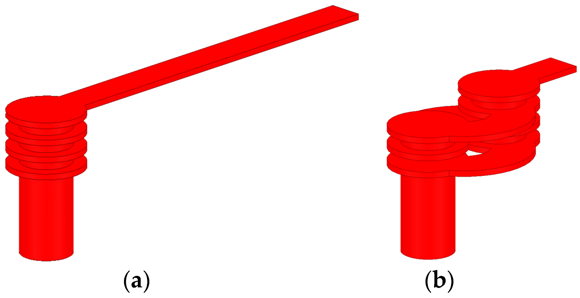
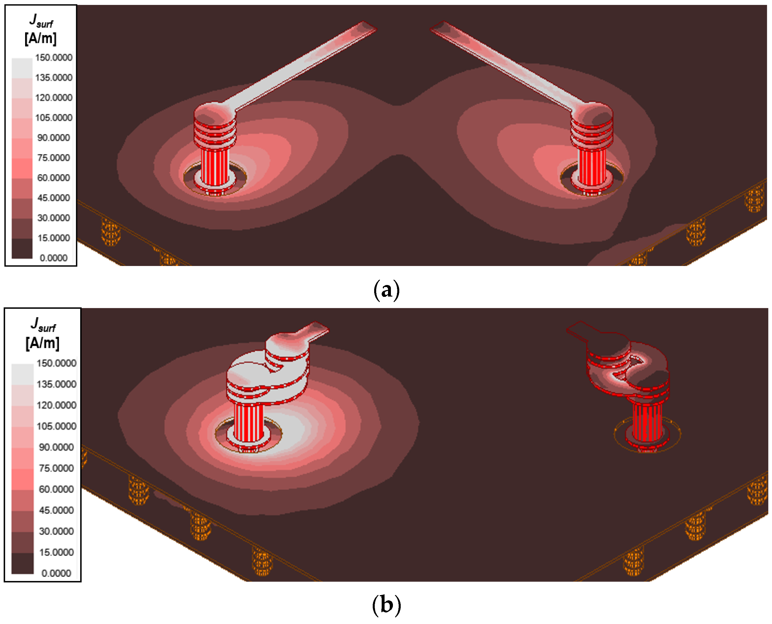
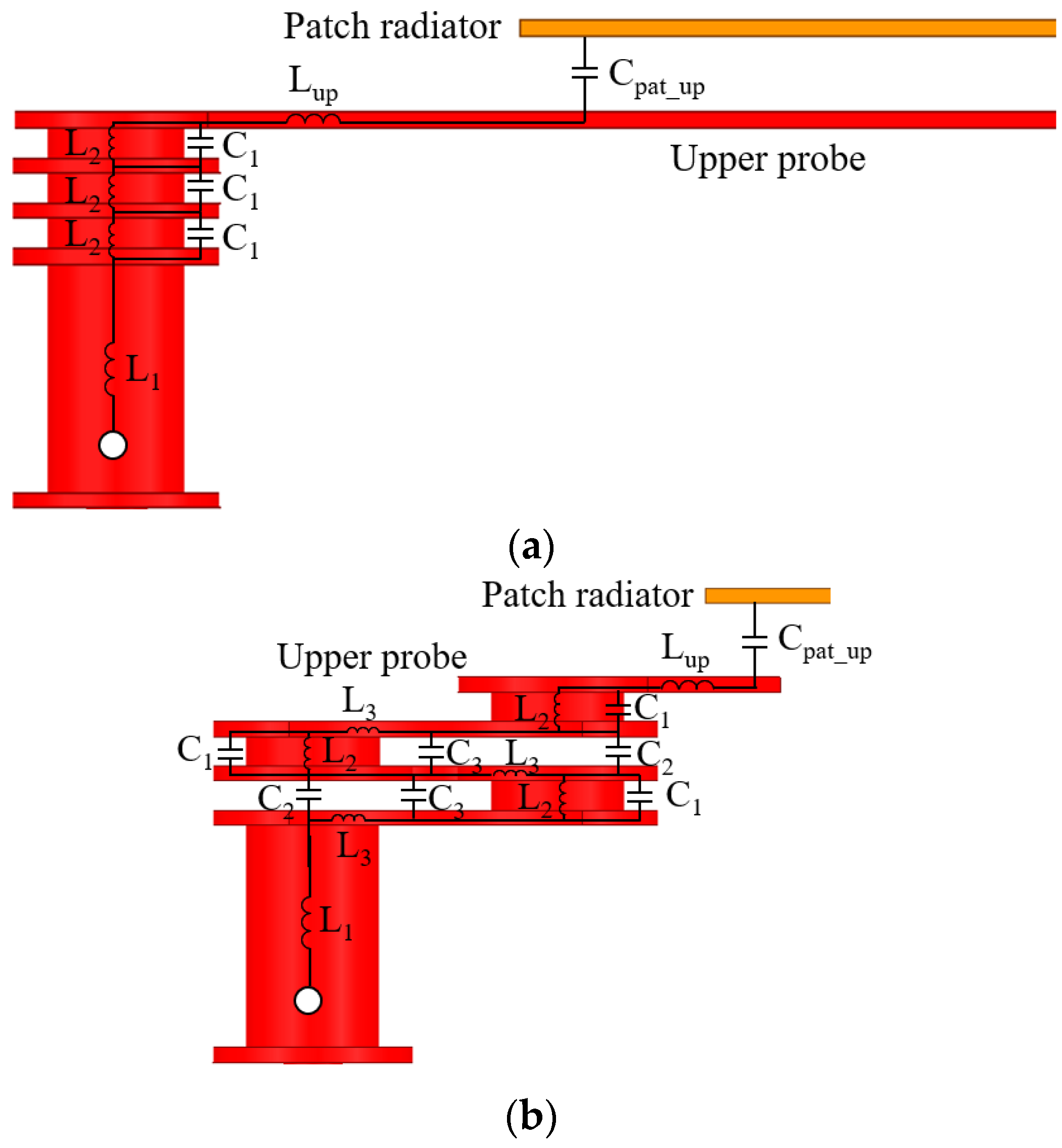
3.1. Conventional L-Probe and Designed Helical-Shaped L-Probe

One well-known method to broaden the bandwidth is the L-probe proximity coupled feeding method, as illustrated in Figure 3a [5,7]. A self-resonance of the feeding structure near the fundamental resonance of the patch antenna can broaden the impedance bandwidth of the L-probe-fed patch antenna [7]. Accordingly, the total length of the L-probe feeding (sum of vertical and horizontal lengths) is an essential parameter in achieving a broad impedance bandwidth. Additionally, the horizontal portion of the conventional L-probe feeding controls the coupling coefficient, i.e., the resonant frequency of the antenna, between the L-probe feeding and the driven patch. Hence, the horizontal portion of the L-probe feeding must have an appropriate length and width. Figure 4a shows the simulated scattering parameters (S-parameters) of the conventional L-probe feeding without a patch radiator. The length of the vertical part of the L-probe feeding is 500 μm in this simulation. The length of the horizontal portion of the L-probe feeding (lPB) varies from 0.9 to 1.5 mm to identify the resonance of the conventional L-probe feeding. As expected, the resonant frequency shifts from 40 to 26 GHz as the lPB increases. When the lPB is 1.5 mm, the L-probe feeding resonates near 27 GHz, close to the center frequency, covering n257, n258, and n261. However, poor isolation between ports is observed in Figure 4a, which is attributed to coupling between ports for V- and H-polarizations. For this reason, the conventional L-probe feeding method is unsuitable for 5G mmWave AiP to realize a broadband dual-polarized antenna.
To address the issue, the HLF is newly designed, as illustrated in Figure 3b. The designed feeding structure consists of a vertical component, which has a helical winding structure with 1.5 turns that is connected between BM1 through TM3, and a horizontal component located at TM4. The designed structure decreases the lPB of the conventional L-probe-fed antenna by 1.2 mm. The simulated resonant frequency of the designed feeding probe is 29.4 GHz.
Regarding the mutual coupling between V- and H-pol ports, a minimum isolation greater than 25 dB between the two ports is achieved due to the decreased lPB, as shown in Figure 4b. Figure 5a,b show the simulated surface current distribution of the conventional and the designed HLF at 27 GHz, respectively, when Port 1 is excited. At the same time, Port 2 is terminated with 50 Ω. The simulated surface current distribution shows the improved isolation between the two ports with the HLF structure replaced by the conventional L probe. A strong surface current is observed from the terminated port (Port 2) in a conventional L-probe structure when Port 1 is excited in Figure 5a. On the other hand, the designed HLF structure shows a negligible coupling effect between ports in Figure 5b.
Figure 6 shows the S-parameters of the conventional L-probe and the designed HLF with a patch radiator. The same rectangular patch radiator of TM6 is used for both L-probes. The resonant frequency of 26 GHz without the patch radiator shifts to 30.5 GHz when the patch radiator is introduced on the conventional L-probe. This is mainly attributed to the capacitance (Cpat_up) between the upper probe and patch radiator in Figure 7a. The high Cpat_up is induced by the coupling between the patch and the conventional L-probe with a longer lPB than the designed L-probe. The feeding position is moved toward the edge of the ground to reduce the coupling, resulting in a larger antenna size. Another method is to shorten the L-probe’s vertical length, increasing the gap between the patch radiator and the horizontal portion of the L-probe. However, this approach requires increased laminated PCB thickness, making manufacturing costly and complex. Therefore, both methods are unsuitable for the low-profile broadband dual-polarized patch antenna. In contrast, the designed dual-polarized patch antenna with an HLF shows a good −10 dB impedance bandwidth of 5.4 GHz (24.2–29.6 GHz) with high isolation (|S21|) greater than 18 dB. The introduction of L3, C2, and C3 in Figure 7b allows a short horizontal portion of the L-probe feeding. Accordingly, the optimal coupling coefficient and high isolation between V- and H-pol ports can be achieved within the limited size and thickness.

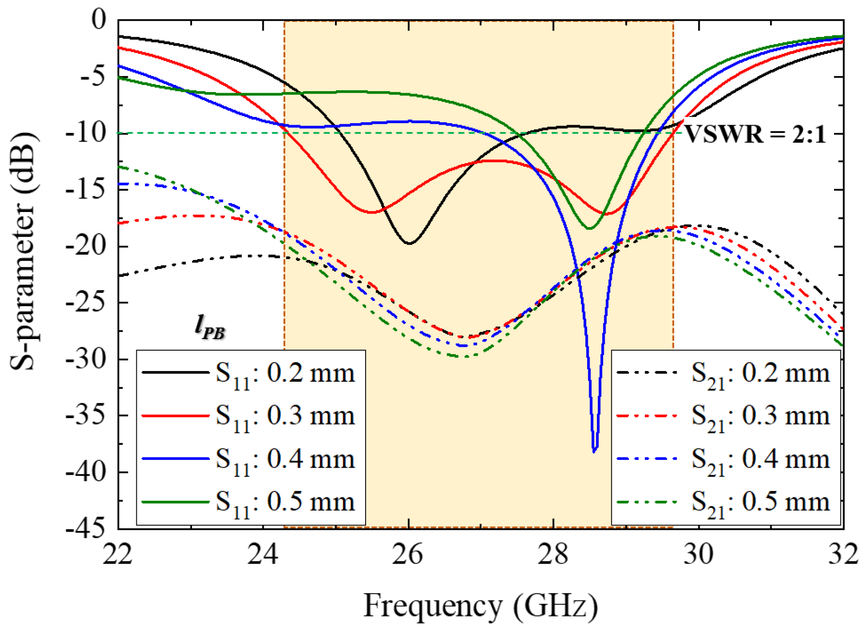
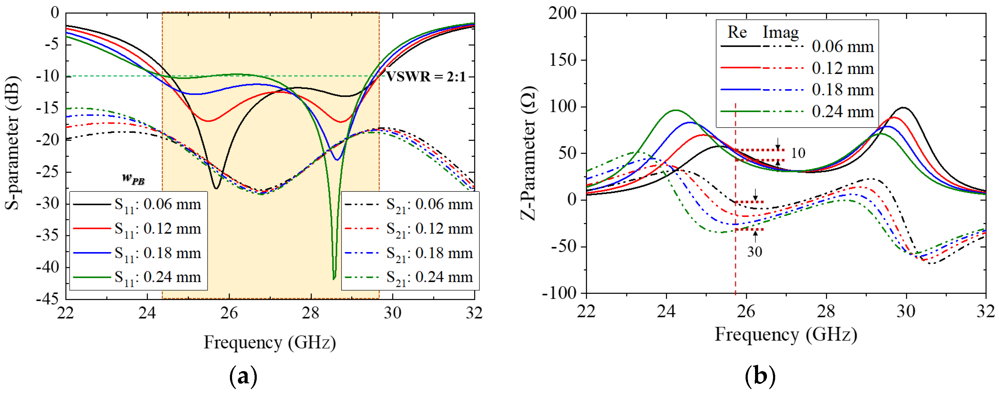
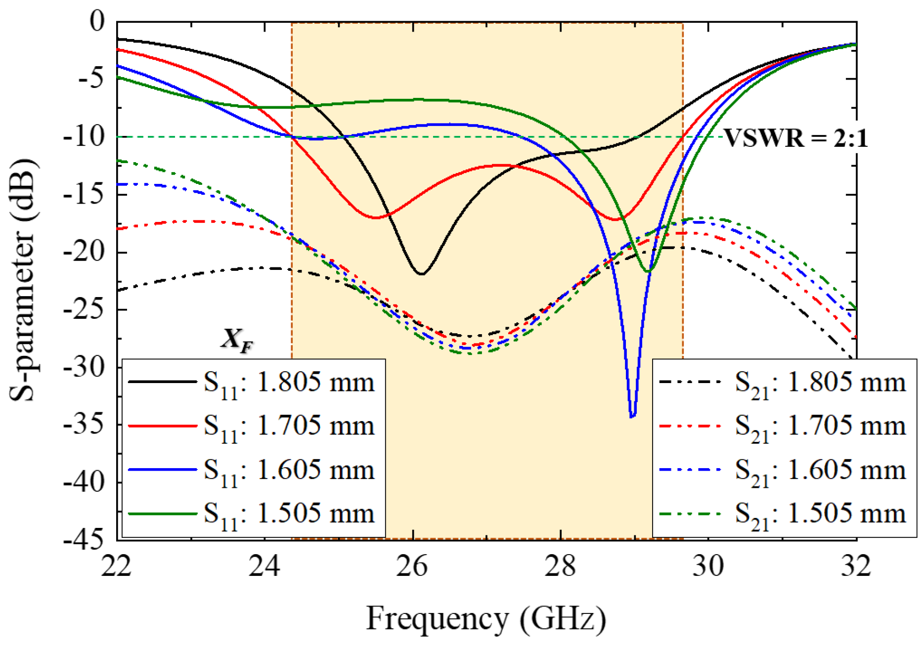
3.2. Parametric Studies on Various HLF Dimensions

Parametric studies on various HLF dimensions were conducted to analyze the effects on antenna performance, determining the optimal HLF dimensions. First, the reflection and transmission characteristics of the designed HLF are analyzed for various lPB of the HLF structure in Figure 8. As the lPB increases from 0.2 to 0.5 mm, the resonance of the S11 shifts from a low to a high frequency. In contrast, the transmission coefficient (S21) is insignificantly affected. Similarly, the resonance of the S11 shifts from a low to a high frequency as the width (wPB) increases from 0.06 to 0.24 mm without changing S21, as shown in Figure 9a. The S11 degrades from −30 to −10 dB in the frequency range between 25 and 26 GHz, while the S11 improves from −12.5 to −40 dB in the frequency ranges between 28.5 and 29 GHz with an increase of wPB.
Antenna input impedance is subject to reactance (Zimag), which is affected by the coupling coefficient between the patch radiator and the horizontal portion of the HLF. Figure 9b shows the simulated resistance and reactance at various wPB values as a function of frequency. The resistance changes within 10 ohms at 25.5 GHz as the wPB varies between 0.06 and 0.24 mm, while the reactance varies within 30 ohms at the same frequency. A lPB of 0.3 mm and wPB of 0.12 mm are chosen for further study, since the antenna with the given dimensions shows good S11 and S21 in the desired frequency bands.
Figure 10 shows the effects of the distance (XF) between the center of the rectangular patch radiator and the center of the stacked via in the CCL for HLF on antenna performance. As the XF decreases from 1.805 to 1.705 mm, the −10 dB impedance bandwidth improves from 4 to 5.2 GHz at the expense of a slightly high S21. However, the impedance matching degrades when XF decreases from 1.705 to 1.505 mm. Therefore, the optimum value of 1.705 mm is selected for XF.
Figure 11 shows the S11 and S21 characteristics of the designed HLF-PA for various diameters of the helical turn (dPB). Good impedance matching is observed in the frequency ranges from 24.2 to 29.6 GHz for a dPB of 0.33 mm. As dPB increases from 0.32 to 0.34 mm, the second resonant frequency (f2) shifts from low to high, which is attributed to the increase in the L3 and total length of the HLF. The simulated results indicate that varying dPB can tune f2.
Figure 12 shows the simulated S-parameter and peak realized gain at boresight (RG00) for the optimized HLF-PA. The HLF-PA shows a wide −10 dB impedance bandwidth of 20% (5.4 GHz: 24.2–29.6 GHz) for both V- and H-pol. High isolation (|SHV|) between V- and an H-pol greater than 18 dB is achieved within the frequency bands of interest. The simulated RG00 ranges from 3.7 to 5.1 dBi in the desired operating frequency bands (24.25–29.6 GHz). Figure 13 shows the electric field distribution at 24.25 GHz and 29.5 GHz. As shown, the patch is well excited with the fundamental mode. Figure 14 shows the 2D radiation patterns of the designed HLF-PA at 24.25 GHz and 29.5 GHz. The simulated maximum gains appear at the boresight in the XOZ and YOZ planes, indicating broad-side radiation for both ports. In addition, the co-polarization for V-pol (Eθ in the XOZ plane and Eϕ in the YOZ plane) is orthogonal to the co-polarization for H-pol (Eϕ in the XOZ plane and Eθ in the YOZ plane) in the same observation plane. Accordingly, the designed HLF-PA exhibits dual-polarization characteristics. Relatively small cross-polarization levels of −20 dB are obtained in the XOZ and YOZ planes.

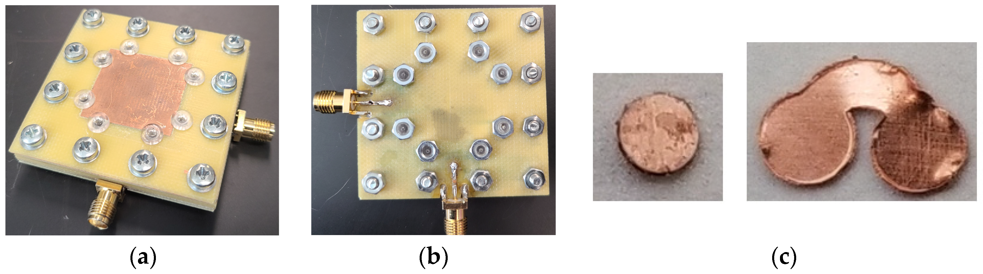
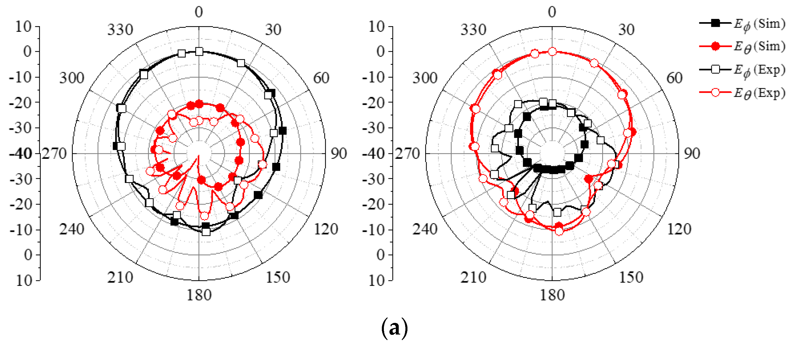
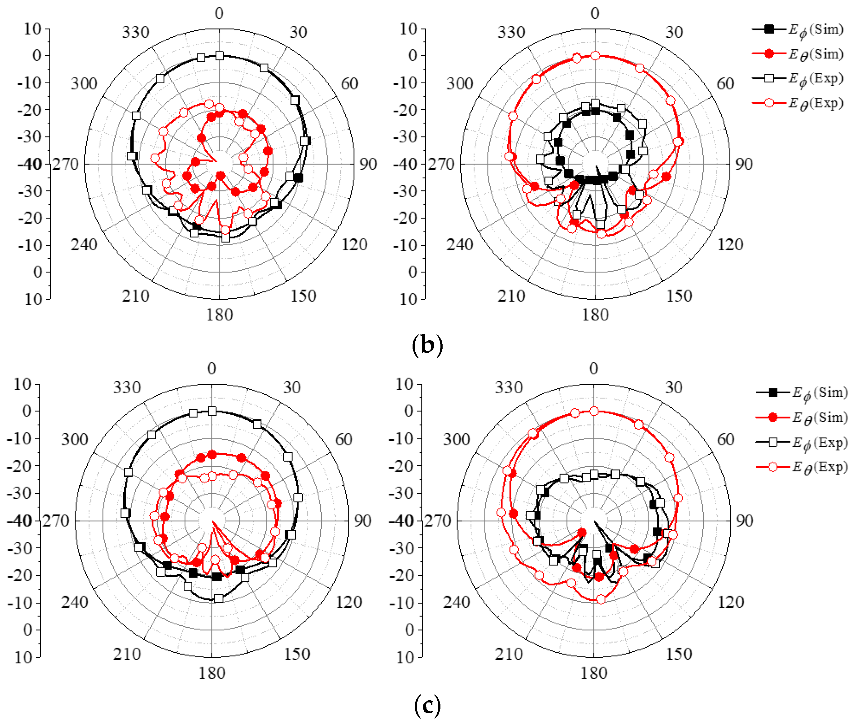
4. 10× Upscaled Antenna Experimental Verification

The 10× upscaled proof-of-concept (PoC) antenna is fabricated and characterized to validate the simulated results based on the structural parameters and specifications in Table 1. Since a multilayer PCB with a fine design rule is inaccessible in small quantities, the designed dual-polarized patch antenna with an HLF structure is upscaled ten times for fabrication to validate the proposed concept. Figure 15 shows the fabricated 10× upscaled PoC antenna. An in-house precision milling machine (LPKF ProtoMat S62, LPKF, Garbsen, Germany) is used to mill eight copper layers of double-sided CCL FR-4 epoxy substrates for each layer. Below is the detailed fabrication process.
  • To align and fully compress the milled substrates into the antenna using M2.5 × 10 mm screws and nuts, 2.55 mm diameter holes were punched on the edges of the substrate and copper patch radiator. M2.5 × 10 mm plastic screws are selected and used on the edge of the copper radiator patch to mitigate the effects of the screws on the radiation from the copper patch radiator.
  • The copper foils of FR-4 substrates were milled accordingly for each TM1–TM6, CCL, BM1, and feeding layer. The purpose of the BM layers is to provide feeding between other chipsets. As shown in Figure 15b, the feeding layer replaces these BM layers to ease the fabrication process and feed. The feeding layer thickness is 0.6 mm, and a microstrip line with a width of 1.2 mm and length of 6.8 mm was used to connect with the probe. Then, portions of the FR-4 substrate were milled to provide spaces to embed parts of the proposed HLF structure for the TM1–TM4 and CCL layers.
  • The individual parts of the proposed HLF structure used in the TM1 to TM4 layers were punched from a 0.2 mm thick copper sheet, as shown in Figure 15c. The copper rod, with a 1.8 mm diameter, connecting between each TM layer and the TM1 and feeding layers, was cut using a diamond wire saw.
  • To integrate the milled substrates and parts of the HLF structure, the FR-4 substrate having the TM1 layer was flipped, and the holes were filled with screws and nuts. After flipping and placing the TM2 layer on top of the TM1 layer, the first copper part of the HLF structure was inserted. Then, the substrate for the TM3 layer was placed on top of the substrate for the TM2 layer. To connect the TM2 and TM3 layers, the copper rod cut in Step 3 was inserted and soldered. Then, the parts for the TM3 layer were included and soldered to connect the copper rod and TM3 layer. This process was repeated to connect the other layers.
  • After stacking all substrates, the bolts were tightened to eliminate possible air gaps between the layers. Then, 50 Ω SMA connectors were used to feed the antennas through feeding layers.
The fabricated 10× upscaled PoC antenna was characterized using a vector network analyzer (VNA: Agilent N5230, Agilent, Santa Clara, CA, USA) for S-parameters and an in-house anechoic chamber (Raymond Quietbox AVS 700, Raymond RF, Cleveland, OH, USA) for radiation patterns and realized gain. The antenna was re-simulated with the upscaled dimensions, modified stack-up, and modified feeding structure to compare the measured and simulated results.
Figure 16 shows the simulated and measured S-parameters and RG00 of the fabricated 10× upscaled PoC antenna. As depicted in Figure 16a, the HLF-PA shows a wide −10 dB impedance bandwidth of 20% (540 MHz: 2.42 GHz~2.96 GHz) for V-pol and 22.7% (620 MHz: 2.42 GHz~3.04 GHz) for H-pol. Further, the high measured |S21| of greater than 18.2 dB is observed. Measured RG00 ranges from 4.0 to 5.2 dBi, closely following the simulated results within ±0.5 dBi, which is approximately the measurement accuracy of the anechoic chamber. Good agreement between the simulated and measured results is observed. Due to the same simulated S11 and S22 values, the solid blue line (S22) covers the solid black line (S11). Small discrepancies between the results may be attributed to minor fabrication errors, frequency-dependent material characteristics, and characterization inaccuracies.
Figure 17 shows the simulated and measured normalized radiation patterns in the E-plane at 2.5, 2.7, and 2.9 GHz for both ports. The measured E-planes show the broadside radiation pattern. The cross-polarization levels are also lower than 15 dB for both ports at all frequencies. These measured results validate the effectiveness of the novel helical L-shaped feeding structure in developing an antenna for 5G mobile devices.

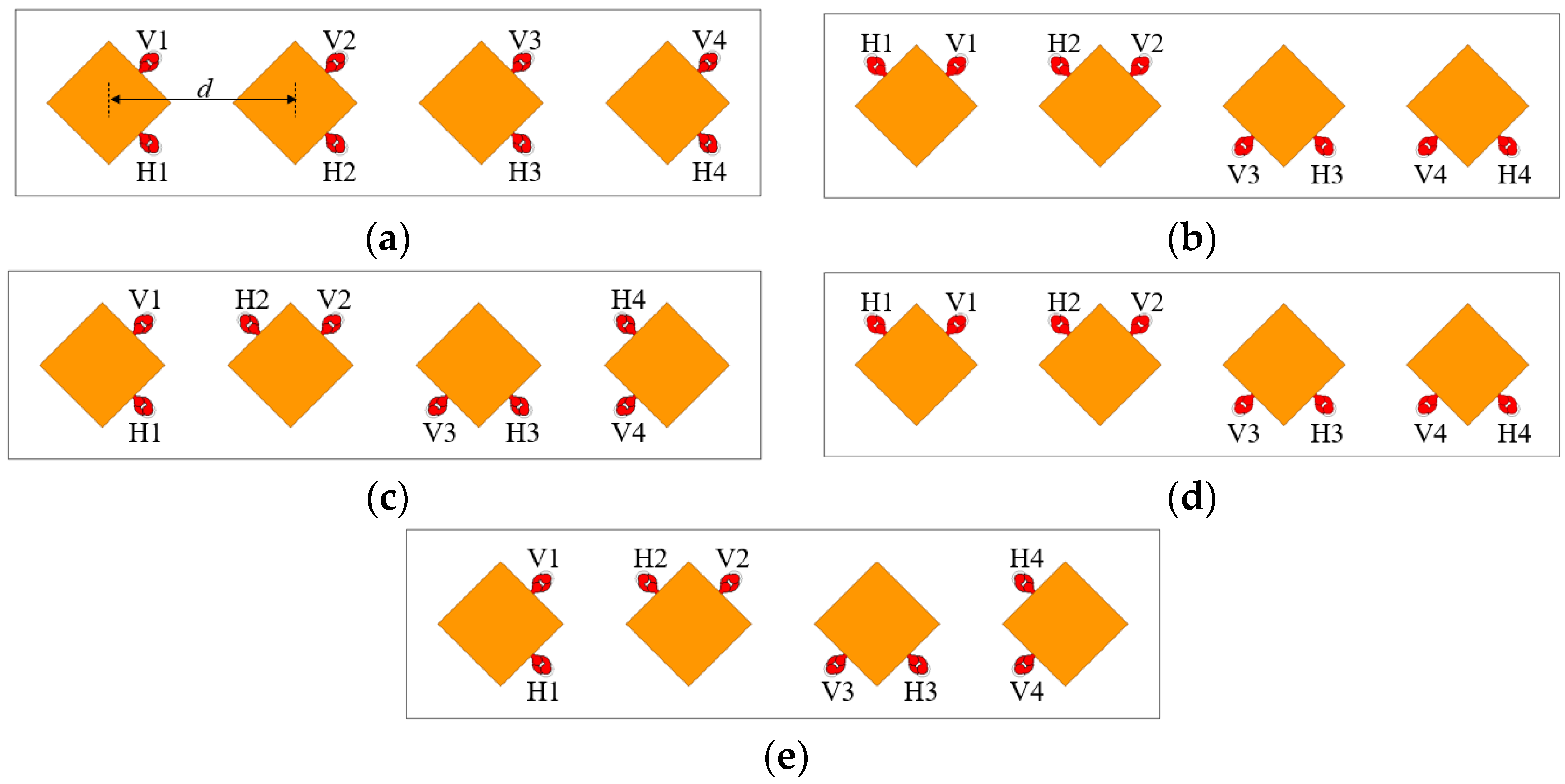
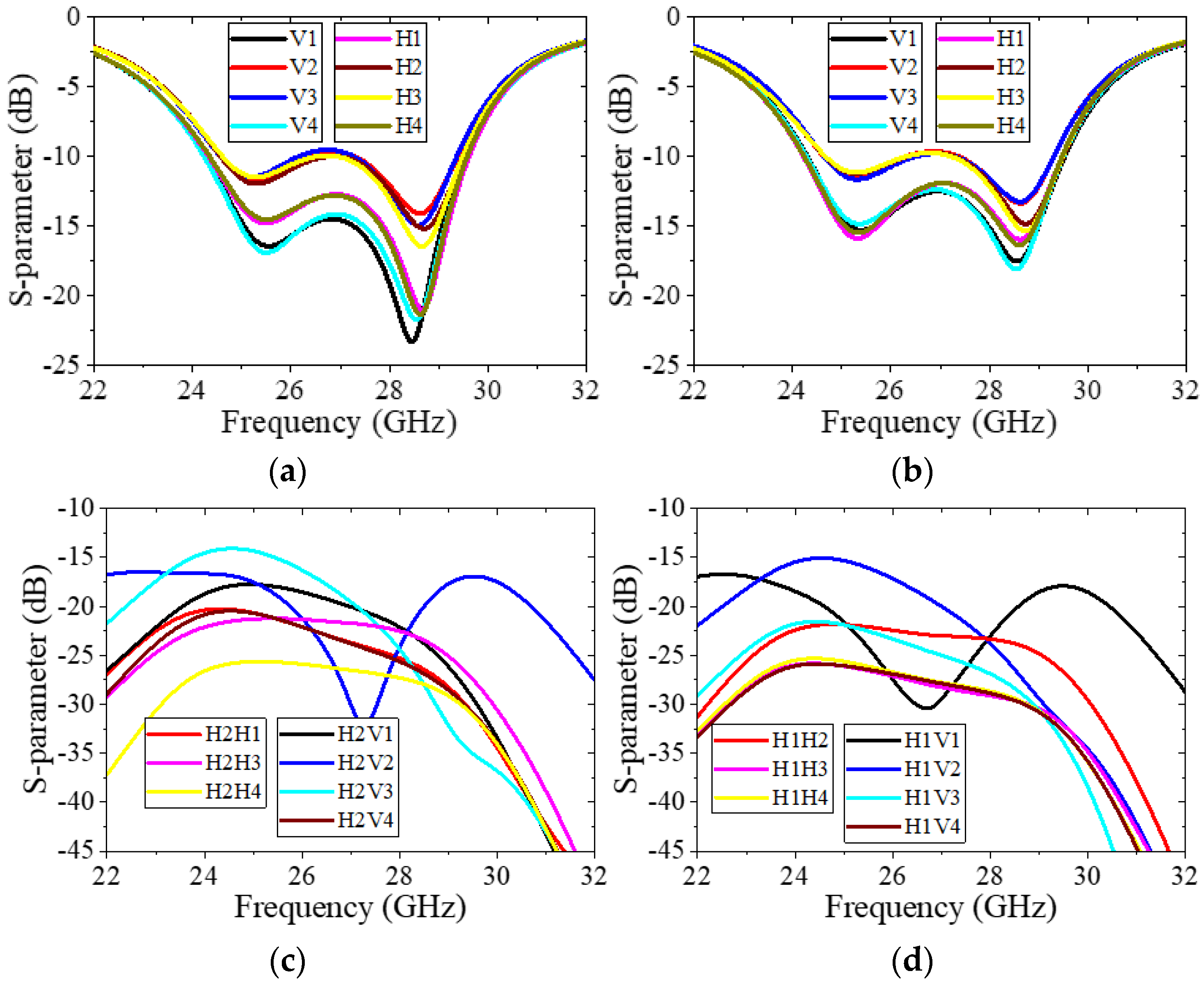
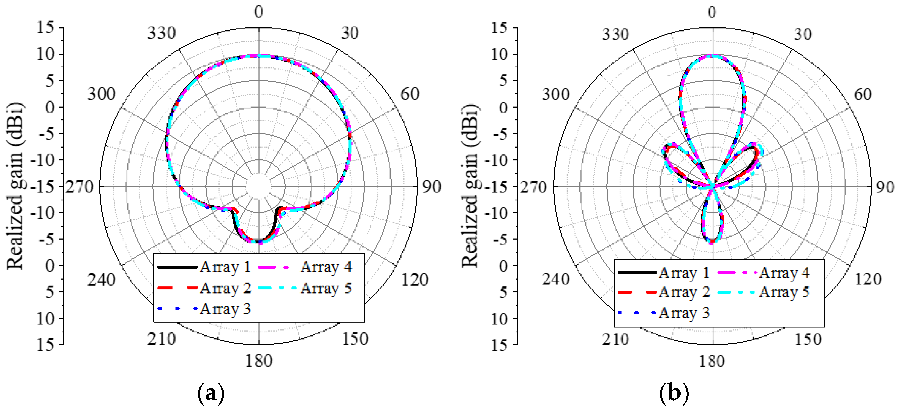
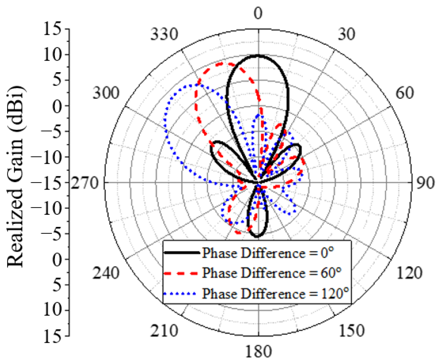
5. Antenna Performance of Antenna Array

The 5G mmWave application requires high antenna gain to overcome propagation path loss at allocated frequencies. Figure 18 shows various designed 1 × 4 HLF-PAAs. The antenna arrays are simulated for performance to validate their versatility and effectiveness in various port configurations. The distance of 5 mm between adjacent elements (d) is used for all port configurations.
The simulated active S-parameters and S21 of the 1 × 4 HLF-PAA with port configuration #2 and #5 are presented in Figure 19. Other arrays show similar antenna performance and are not presented. A broad −10 dB impedance bandwidth is observed from the simulated S-parameters of HLF-PAA with port configurations #2 and #5, which can cover the low band of 5G NR FR2. The impedance matching is slightly degraded compared to the impedance matching of the optimized unit antenna. This is because the minimum port-to-port isolation is marginally degraded from 18 to 15 dB within the operating frequency in Figure 19b.
The simulated far-field characteristics of the 1 × 4 HLF-PAA are presented in Figure 20, Figure 21 and Figure 22. The simulated frequency-dependent RG00 of 1 × 4 HLF-PAAs for all port configurations is shown in Figure 20. The simulated lowest RG00 of all HLF-PAAs is 8.5 dBi in the operating frequency bands. The maximum RG00 is 10 dBi. Thus, the simulated result demonstrates that the proposed L-probe structures can be used in any array configuration without any significant degradation of bandwidth and isolation. Figure 21 shows the simulated radiation patterns of the developed 1 × 4 HLF-PAAs with the excitation of V-pol ports in XOZ- and YOZ-plane at 27 GHz. The HLF-PAAs exhibit good broadside radiation at both observation planes.
The beamforming capability of HLF-PAA is validated by varying the phase progression angle from 0° to 120°. The simulated 2D radiation patterns of the HLF-PAA with port configuration #1, when only V-po. ports were excited at 27 GHz, are shown in Figure 22 for the phase progression angle from 0° to 120°. As the angle varies from 0° to 120°, the angle for the maximum gain from the radiation pattern in the YOZ plane was steered from 0° to 318° in Figure 22. Low sidelobe levels (SLLs) less than 9.3 dB are observed. Other HLF-PAAs show the same beamforming capability. It is also noted that the far-field characteristics of the HLF-PAA with the excitation of H-pol. ports show identical performance (not shown here) due to the structural symmetry. Thus, it can be concluded that the developed HLF-PAA is insensitive to the port configuration, which can increase the level of design freedom.
Table 2 summarizes that the designed HLF-PA is compared with previously reported antennas for 5G mmWave applications. The HLF-PA is the only low-cost antenna that shows a wide impedance bandwidth (5.4 GHz: 24.2–29.6 GHz) covering n257, n258, and n261 of the 5G NR FR2, antenna peak gain above 5 dBi, dual polarization, and thickness below 600 μm, compared to other reported antennas. To emphasize the effectiveness of the proposed antenna, the boxes highlighted in green are antennas that show bandwidth above 20%, gain higher than 5 dBi, a low-cost substrate, thickness below 600 μm, and the dual-polarization feature, while the boxes highlighted in red are antennas that do not meet the above requirements.

6. Conclusions

A novel dual-polarized helical-shaped L-probe fed patch antenna (HLF-PA) and phased array (HLF-PAA) were designed to cover n257, n258, and n261 for the 5G new radio (NR) frequency range 2 (FR2). The antenna has a wide impedance bandwidth (>5.4 GHz), excellent isolation between V- and H-ports (|SHV| > 18 dB), and good antenna gain (up to 5.1 dBi) with a small height of 600 um for the antenna portion in the antenna-in-package (AiP). The optimized 10× upscaled AiP was fabricated to compare the measured antenna performance with the simulated results. The measured and simulated results show a good agreement. Various 1 × 4 phased arrays were designed based on the optimized single element. The designed 1 × 4 HLF-PAAs showed reasonable isolation between ports (|Sij| > 15 dB) and excellent antenna gain with good impedance matching in the desired 5G NR FR2. The developed HLF-PAA has also demonstrated beamforming capabilities, which are vital for 5G wireless communication. Therefore, the designed antenna holds promise in 5G mobile devices.

7. Patents

One U.S. patent entitled “Wideband millimeter (mmWave) antenna” is granted by the U.S. patent office.

Author Contributions

Conceptualization, W.L.; methodology, W.L.; software, W.L. and H.W.; validation, W.L. and H.W.; formal analysis, W.L. and H.W.; investigation, W.L. and H.W.; resources, Y.-K.H.; data curation, W.L. and H.W.; writing—original draft preparation, W.L. and H.W.; writing—review and editing, W.L., H.W., Y.-K.H., M.C. and S.-Y.A.; visualization, H.W.; supervision, Y.-K.H.; project administration, Y.-K.H.; funding acquisition, Y.-K.H. All authors have read and agreed to the published version of the manuscript.

Funding

This work was supported by the NSF under grant number 2137275 and the E. A. “Larry” Drummond Endowment at the University of Alabama.

Data Availability Statement

The data presented in this study are available on request from the corresponding author due to university restrictions.

Conflicts of Interest

Author Woncheol Lee was employed by the company Samsung Electronics. Author Sung-Yong An was employed by the company Samsung Electro-Mechanics Co., Ltd. The remaining authors declare that the research was conducted in the absence of any commercial or financial relationships that could be construed as a potential conflict of interest.

References

  1. Making 5G NR a Commercial Reality: A Unified, More Capable 5G Air Interface. Available online: https://www.qualcomm.com/media/documents/files/making-5g-nr-a-commercial-reality.pdf (accessed on 6 June 2019).
  2. Liu, D.; Gu, X.; Baks, C.W.; Valdes-Garcia, A. Antenna-in-Package Design Considerations for Ka-band 5G Communication Applications. IEEE Trans. Antennas Propag. 2017, 65, 6372–6379. [Google Scholar] [CrossRef]
  3. Gu, X.; Liu, D.; Baks, C.; Tageman, O.; Sadhu, B.; Hallin, J.; Rexberg, L.; Valdes-Garcia, A. A Multilayer Organic Package with 64 Dual-polarized Antennas for 28 GHz 5G Communications. In Proceedings of the 2017 IEEE MTT-S International Microwave Symposium (IMS), Honololu, HI, USA, 4–9 June 2017; pp. 1899–1901. [Google Scholar] [CrossRef]
  4. Du, J.-K.; So, K.; Ra, Y.; Jung, S.-Y.; Kim, J.; Kim, S.Y.; Woo, S.; Kim, H.-T.; Ho, Y.-C.; Paik, W. Dual-polarized Patch Array Antenna Package for 5G Communication Systems. In Proceedings of the 2017 11th European Conference on Antennas and Propagation (EUCAP), Paris, France, 19–24 March 2017; pp. 3493–3496. [Google Scholar]
  5. Mak, C.; Luk, K.; Lee, K.; Chow, Y. Experimental Study of a Microstrip Patch Antenna with L-shaped Probe. IEEE Trans. Antennas Propag. 2000, 48, 777–783. [Google Scholar] [CrossRef]
  6. Xue, M.; Wan, W.; Wang, Q.; Cao, L. Low-profile Wideband Millimeter-wave Antenna-in-Package Suitable for Embedded Organic Substrate Package. IEEE Trans. Antennas Propag. 2021, 69, 4401–4411. [Google Scholar] [CrossRef]
  7. Hazdra, P.; Mazanek, M.; Cermak, J. Wideband Rectangular Microstrip Patch Antenna using L-probe Feeding System. Radioengineering 2007, 16, 37–41. [Google Scholar]
  8. Hong, W.; Baek, K.-H.; Goudelev, A. Grid Assembly-Free 60-GHz Antenna Module Embedded in FR-4 Transceiver Carrier Board. IEEE Trans. Antennas Propag. 2013, 61, 1573–1580. [Google Scholar] [CrossRef]
  9. Kim, W.; Bang, J.; Choi, J. A Cost-effective Antenna-in-Package Design with a 4 × 4 Dual-polarized High Isolation Patch Array for 5G mmWave Applications. IEEE Access 2021, 9, 163882–163892. [Google Scholar] [CrossRef]
  10. Guo, G.; Wu, L.-S.; Zhang, Y.-P.; Mao, J.-F. Stacked Patch Array in LTCC for 28 GHz Antenna-in-Package Applications. In Proceedings of the 2017 IEEE Electrical Design of Advanced Packaging and Systems Symposium (EDAPS), Haining, China, 14–16 December 2017; pp. 1–3. [Google Scholar]
  11. Guo, J.; Hu, Y.; Hong, W. A 45° Polarized Wideband and Wide-Coverage Patch Antenna Array for Millimeter-Wave Communication. IEEE Trans. Antennas Propag. 2021, 70, 1919–1930. [Google Scholar] [CrossRef]
  12. Gu, X.; Liu, D.; Hasegawa, Y.; Masuko, K.; Baks, C.; Suto, Y.; Fujisaku, Y.; Sadhu, B.; Paidimarri, A.; Guan, N.; et al. Antenna-in-Package Integration for a Wideband Scalable 5G Millimeter-Wave Phased-Array Module. IEEE Microw. Wirel. Compon. Lett. 2022, 31, 682–684. [Google Scholar] [CrossRef]
  13. Seo, J.; Yoon, I.; Jung, J.; Ryoo, J.; Park, J.; Lee, W.; Ko, D.; Oh, J. Miniaturized Dual-Band Broadside/Endfire Antenna-in-Package for 5G Smartphone. IEEE Trans. Antennas Propag. 2021, 69, 8100–8114. [Google Scholar] [CrossRef]
  14. Lu, R.; Yu, C.; Wu, F.; Yu, Z.; Zhu, L.; Zhou, J.; Yan, P.; Hong, W. SIW Cavity-Fed Filtennas for 5G Millimeter-Wave Applications. IEEE Trans. Antennas Propag. 2021, 69, 5269–5277. [Google Scholar] [CrossRef]
  15. Chang, Y.C.; Hsu, C.-C.; Magray, M.I.; Hsu, Y.-C.; Tarng, J.-H. Wideband and Low Profile Miniaturized Magneto-Electric Dipole Antenna for 5G mmWave Applications. In Proceedings of the 2020 IEEE Asia-Pacific Microwave Conference (APMC 2020), Hong Kong, China, 10–13 November 2020. [Google Scholar]
  16. Kim, G.; Kim, S. Design and Analysis of Dual Polarized Broadband Microstrip Patch Antenna for 5G mmWave Antenna Module on FR4 Substrate. IEEE Access 2021, 9, 64306–64316. [Google Scholar] [CrossRef]
  17. Park, J.; Choi, D.; Hong, W. Millimeter-wave Phased-array Antenna-in-Package (AiP) using Stamped Metal Process for Enhanced Heat Dissipation. IEEE Antennas Wirel. Propag. Lett. 2019, 18, 2355–2359. [Google Scholar] [CrossRef]
  18. Chou, H.-T.; Chou, S.-J.; Deng, J.D.S.; Chang, C.-H.; Yan, Z.-D. LTCC-based Antenna-in-Package Array for 5G User Equipment with Dual-polarized Endfire Radiations at Millimeter-wave Frequencies. IEEE Trans. Antennas Propag. 2021, 70, 3076–3081. [Google Scholar] [CrossRef]
  19. Yu, B.; Qian, Z.; Lin, C.; Lin, J.; Zhang, Y.; Yang, G.; Luo, Y. A Wideband mmWave Antenna in Fan-Out Wafer Level Packaging With Tall Vertical Interconnects for 5G Wireless Communication. IEEE Trans. Antennas Propag. 2021, 69, 6906–6911. [Google Scholar] [CrossRef]
  20. Li, H.; Li, Y.; Chang, L.; Sun, W.; Qin, X.; Wang, H. A Wideband Dual-Polarized Endfire Antenna Array With Overlapped Apertures and Small Clearance for 5G Millimeter-Wave Applications. IEEE Trans. Antennas Propag. 2021, 69, 815–824. [Google Scholar] [CrossRef]
  21. Zhang, H.; Shamim, A. Wideband and Wide Beam Scanning Dual-Polarized Phased Array Antenna-in-Package Design for 5G Applications. IEEE Open J. Antennas Propag. 2024, 5, 140–152. [Google Scholar] [CrossRef]
  22. Kim, G.; Kim, D.; Lim, K.; Yang, C.; You, C.; Kim, S. Dual-band Dual-polaried Rhombic Patch Antenna Array for 5G mmWave RF Front End Antenna-in-Package Module. IEEE Antennas Wirel. Propag. Lett. 2024, 23, 2120–2124. [Google Scholar] [CrossRef]
  23. Yin, Y.; Xia, C.; Liu, S.; Zhang, Z.; Chen, C.; Wang, G.; Wang, C.; Wu, Y. Ultrathin Antenna-in-Package Based on TMV-Embedded FOWLP for 5G mm-Wave Applications. Electronics 2024, 13, 839. [Google Scholar] [CrossRef]
Figure 1. The 5G frequency band allocations across the world in millimeter wave bands [1].
Electronics 13 03119 g001
Figure 2. Geometry and dimensions of the proposed (a) dual-polarized helical-shaped L-probe fed patch antenna (HLF-PA) and (b) PCB stack-up of the designed HLF-PA.
Electronics 13 03119 g002
Figure 3. Geometry of (a) the conventional L-probe and (b) the designed helical-shaped L-probe structure.
Electronics 13 03119 g003
Figure 4. Simulated S-parameters: (a) conventional L-probe with various lPB and (b) designed helical-shaped L-probe without the patch radiator.
Electronics 13 03119 g004
Figure 5. Simulated surface current density distribution of (a) the conventional L-probe and (b) the designed helical-shaped L-probe without the patch radiator at 27 GHz.
Electronics 13 03119 g005
Figure 6. Simulated S-parameters of the conventional L-probe and the designed helical-shaped L-probe with a patch radiator.
Electronics 13 03119 g006
Figure 7. Equivalent circuit of (a) the conventional L-probe and (b) the designed helical-shaped L-probe.
Electronics 13 03119 g007
Figure 8. Simulated S-parameters of the designed helical-shaped L-probe with various lPB.
Electronics 13 03119 g008
Figure 9. Simulated (a) S- and (b) Z-parameters of the designed helical-shaped L-probe with various wPB in mm.
Electronics 13 03119 g009
Figure 10. Simulated S-parameters of the designed helical-shaped L-probe with various XF.
Electronics 13 03119 g010
Figure 11. Simulated frequency-dependent S-parameters of the designed helical-shaped L-probe with various dPB.
Electronics 13 03119 g011
Figure 12. Simulated frequency-dependent S-parameters and peak realized gain at boresight of the designed dual-polarized patch antenna with the helical-shaped L-probe feeding.
Electronics 13 03119 g012
Figure 13. Electric field distribution at (a) 24.25 GHz and (b) 29.5 GHz.
Electronics 13 03119 g013
Figure 14. Simulated radiation patterns of the designed dual-polarized patch antenna with the helical-shaped L-probe feeding at 24.5 and 29.5 GHz: V-pol (a) XOZ and (b) YOZ plane and H-pol (c) XOZ and (d) YOZ plane.
Electronics 13 03119 g014
Figure 15. Photo images of the fabricated 10× upscaled dual-polarized patch antenna with the helical-shaped L-probe: (a) overall, (b) bottom (feeding layer), and (c) parts of helical-shaped L-probe: via (left) and helical-shaped pattern (right). (The 2.92 mm (K-type) connector is suitable for n257, n258, and n261 bands.)
Electronics 13 03119 g015
Figure 16. Simulated and measured (a) S-parameters and (b) peak realized gain of the 10× upscaled fabricated dual-polarized patch antenna with modified L-probe.
Electronics 13 03119 g016
Figure 17. Simulated and measured normalized radiation pattern of 10× upscaled designed dual-polarized patch antenna with modified L-probe at (a) 2.5, (b) 2.7, and (c) 2.9 GHz.
Electronics 13 03119 g017aElectronics 13 03119 g017b
Figure 18. Design of 1 × 4 designed wideband dual-polarized 5G antenna array with different port configuration: array (a) #1, (b) #2, (c) #3, (d) #4, and (e) #5.
Electronics 13 03119 g018
Figure 19. Simulated S11 of 1 × 4 wideband dual-polarized 5G antenna array configuration (a) #2 and (b) #5 and S21 of array (c) #2 and (d) #5.
Electronics 13 03119 g019
Figure 20. Simulated peak realized gain of 1 × 4 HLF-PAAs.
Electronics 13 03119 g020
Figure 21. Simulated realized gain radiation pattern of 1 × 4 HLF-PA arrays at 27 GHz with d of 5 mm: (a) XOZ and (b) YOZ plane.
Electronics 13 03119 g021
Figure 22. Simulated realized gain radiation pattern of 1 × 4 HLF-PA array at 27 GHz with d of 5 mm and different phase progression at YOZ planes.
Electronics 13 03119 g022
Table 1. Dimensions of wideband dual-polarized 5G mmWave patch antenna structure.
lSwSlPwPlPBwPBdFdFPdPB
552.352.350.30.120.180.270.33
wHPXFdVdVPdctPPGtCCLtCuUnit in mm
0.1451.7050.080.120.50.060.30.02
Table 2. Performance comparison between state-of-the-arts and developed antenna *.
Ref.Frequency Band
(−10 dB Bandwidth)
Peak Element GainSubstrateHeight for Antenna PartRemark
[2]30–30.8 GHz
(0.8 GHz: 2.6%)
3 dBi2 HDIsN. G.Dual-pol
(|Sij| > 22 dB)
[3]26.3–30 GHz
(3.7 GHz: 13%)
4 dBiAir cavity and 2 HDIsN. G.Dual-pol
(|Sij|: N. G.)
[4]27.4–29.6 GHz
(2.2 GHz: 7.7%)
4.5 dBi3 HDIs490 μm
(0.045 λL)
Dual-pol
(|Sij|: N. G.)
[5]26.4–29.3 GHz
(2.9 GHz: 10%)
N. G.A6 LTCC480 μm
(0.042 λL)
Single-pol
(|Sij|: N. A.)
[6]22.8–33.3 GHz
(10.5 GHz: 37.5%)
N. G.Organic substrate (HL972LF, GHPL-970LF)420 μm
(0.031 λL)
Single-pol
(|Sij|: N. A.)
[9]26.5–29.5 GHz
(3.0 GHz: 11%)
7.4 dBiTLY-5 and FR-41200 μm
(0.11 λL)
Dual-pol
(|Sij| > 23 dB)
[11]22.3–29.6 GHz
(7.3 GHz: 28%)
5.8 dBiTLY-5, FR-27, FR-4, RO43502570 μm
(0.2 λL)
Single-pol
(|Sij|: N. A.)
[14]24.25–29.5 GHz
(5.25 GHz: 20%)
4.5 dBiRO4003C, RO4450F, TLY-51800 μm
(0.15 λL)
Dual-pol
(|Sij| > 35 dB)
[16]23-29 GHz
(6 GHz: 23.1%)
5 dBiFR-4, Air1200 μm
(0.092 λL)
Dual-pol
(|Sij| > 15 dB)
[18]27.5–31 GHz
(3.5 GHz: 12%)
6 dBiLTCC1183 μm
(0.11 λL)
Dual-pol
(|Sij| > 14 dB)
[21]25.87–29.05 GHz
(3.18 GHz: 11.5%)
N. G.RO3003 and RO40031100 μm
(0.095 λL)
Single-pol
(|Sij|: N. A.)
[22]26–31.0 GHz
(5.0 GHz: 17.5%)
N. G.Prepreg1160 μm
(0.1 λL)
Dual-pol
(|Sij| > 10 dB)
[23]24.2–28.5 GHz
(4.3 GHz: 17.8%)
7.5 dBiEMC, Dielectric polymer450 μm
(0.036 λL)
Single-pol
(|Sij| > N. A.)
This work24.2–29.6 GHz
(5.4 GHz: 20%)
5.1 dBiFR-4600 μm
(0.048 λL)
Dual-pol
(|Sij| > 18 dB)
* N. G.: not given; N. A.: not applicable; λL is the air wavelength at lowest frequency.
Disclaimer/Publisher’s Note: The statements, opinions and data contained in all publications are solely those of the individual author(s) and contributor(s) and not of MDPI and/or the editor(s). MDPI and/or the editor(s) disclaim responsibility for any injury to people or property resulting from any ideas, methods, instructions or products referred to in the content.

