Article

Design Optimization of a THz Receiver Based on 60 nm Complementary Metal–Oxide–Semiconductor Technology

by
Fabrizio Palma
1,*,
Demetrio Logoteta
1,
Francesco Centurelli
1,
Pascal Chevalier
2,
Renato Cicchetti
1,
Frederic Monsieur
2,
Carlo Santini
1,
Orlandino Testa
1,
Alessandro Trifiletti
1 and
Antonio d’Alessandro
1
1
DIET, Università di Roma La Sapienza, 00184 Rome, Italy
2
STMicroelectronics, Technology & Design Platforms, 850 Rue Jean Monnet, 38920 Crolles, France
*
Author to whom correspondence should be addressed.
Electronics 2024, 13(16), 3122; https://doi.org/10.3390/electronics13163122
Submission received: 14 June 2024 / Revised: 30 July 2024 / Accepted: 31 July 2024 / Published: 7 August 2024
(This article belongs to the Special Issue Advanced Topics in Modelling Microwave and mmWave Electron Devices)

Abstract

:
The technology transfer of terahertz wireless communication from research laboratories to commercial applications is a global strategic achievement currently pursued to match the ever-increasing demand for high-speed communication. The use of commercial integrated electronics for the detection of THz waves is an intriguing challenge which has enticed great interest in the scientific research community. Rapid progress in this field has led to the exploitation of THz direct detection using standard CMOS technology based on the so-called self-mixing effect. Our research, stemming out of a collaboration between Sapienza University of Rome and STMicroelectronics company, is focused on the complete design process of a THz rectifier, realized using 50 nm ST B55 CMOS technology. In this paper, we report the optimization process of a case-study receiver, aimed to demonstrate the feasibility of direct demodulation of the transmitted OOK signal. A relatively limited bandwidth extension is considered since the device will be included in a system adopting a radiation source with a limited band. The design refers to a specific technology, the 60 nm MOS in B55X ST; nevertheless, the proposed optimization procedure can be applied in principle to any MOS device. Several aspects of the rectification process and of the receiver design are investigated by combining different numerical simulation methodologies. The direct representation of the rectification effect through the equivalent circuit of the detector is provided, which allows for the investigation of the detector–amplifier coupling, and the computation of output noise equivalent power. Numerical results are presented and used as the basis for the optimization of the receiver parameters.

1. Introduction

The terahertz (THz) radiation spectrum spans what, in current applications, appears as a gap between microwaves and infrared frequencies. THz radiation is considered medically safe since it is non-ionizing and the associated RF power density is generally low. At THz frequencies, the radiation can deeply scan under the surface of objects, materials, and packaging. The resulting combination of safety and wave penetration makes THz a powerful tool in various applications, such as security/surveillance imaging, medical imaging, nondestructive tests, and spectroscopic applications. However, the use of integrated commercial electronics for the detection of high-frequency electromagnetic radiation, especially in the THz frequency range, is still an open challenge. This goal is driving significant experimental and theoretical activities with demanding requirements to achieve new cameras in the THz spectrum, offering high-resolution images characterized by high sensitivity and low cost. Furthermore, the data rate of wireless communications in commercial markets is expected to reach 100 Gbps within the next 10 years. Accordingly, the bands above 100 GHz are seen by many as the next frontier in wireless communications. Thus, evolution of terahertz (THz) wireless communication technologies, moving from research laboratories to commercial applications, will represent an extremely important achievement to be pursued in the near future.
Recently, there has been a strong effort to realize THz detectors using standard complementary metal–oxide–semiconductor (CMOS) technology. Several works that highlight the exceptionally rapid progress of THz science and technology in this particular area are reported in [1,2,3,4,5,6,7,8,9,10,11,12,13,14,15,16,17].
Rectification of high-frequency radiation occurs in an MOS structure because of the interaction between the charge carriers and the THz field. The rectification originates from the so-called self-mixing effect due to the nonlinearities in the semiconductor transport equations and resulting in a mixing of quantities proportional to the first order to the antenna voltage amplitude.
The mechanisms of quadratic rectification in the MOS transistors, under very high frequency stimulus, is traditionally described based on the model of plasma waves in the channel [18]. This model is still routinely employed in detector design [19,20] despite the cut-off frequency of the device being dramatically lower than the detected THz frequency and several experiments have demonstrated its strong limitations.
Recently, the rectification of high-frequency voltage signals in MOS was described following a new approach, [21], which demonstrates that the self-mixing process occurs within the potential barriers possibly present in a silicon device. This new model can be essential to interpret the physical origin of the self-mixing effect and to derive a reliable design procedure.
Upon the self-mixing effect, the rectified DC potential is proportional to the square of the THz wave amplitude. There is therefore no need for local oscillators in the reception process.
In this paper, we present a complete design procedure of a THz rectifier realized with CMOS technology. The design is carried out by using, as intermediate checks, simulations of the transistor structure performed by the Technology Computer-Aided Design (TCAD) Sentaurus™ Device software suite [22].
The use of the TCAD simulator to explain the MOS rectification process has already been reported in the literature within different approaches and with different results. In [23], the characterization was carried out in the transient regime by evaluating the time-domain drain voltage and then extracting the DC and harmonic components of the drain voltage through a Fourier transform. In [24,25], the capability of TCAD Sentaurus to treat the quasi-2D plasma behavior was used, with the specific purpose to limit the interaction occurring between the charge carriers and the THz field in the channel zone. In [26], the bell-shaped response of the voltage at the drain versus the gate–source bias voltage was extracted from two-dimensional simulations. The authors themselves have performed extensive simulations to achieve an understanding of the behavior of the semiconductor structure in an MOS transistor at such a high frequency [27,28]. To this end, Harmonic Balance (HB) analysis [29], which precisely describes the nonlinear processes stemming from the nonlinearities of semiconductor equations, was adopted. Despite its potential, this approach has received so far little attention from the THz community.
The self-mixing process, the origin of the rectification process in MOS transistors, is intrinsically very fast since the majority carriers of the doped regions of the semiconductor structure are involved in the non-linear interaction with the high-frequency electric field [30]. The rectified potential, generated beside the source–gate edges, must propagate along the transistor structure as far as the drain terminal. Although a time delay is expected due to the charging process of the parasitic capacitances of the structure, it is certainly compatible with the demodulated signal bandwidth, given the reduced size of the actual CMOS devices. Moreover, this important issue was analyzed by the authors using the new model and TCAD simulations [30].
The methods adopted to investigate the rectification process are described in Section 2. In Section 3, the results of numerical simulations are presented and discussed. Particularly, we derive and use the equivalent circuit of the detector as a direct representation of the rectification effect. This equivalent circuit will be the basis for the calculation of the noise-equivalent power and the optimization of the receiver parameters.

2. Materials and Methods: Analysis of the Detection Process

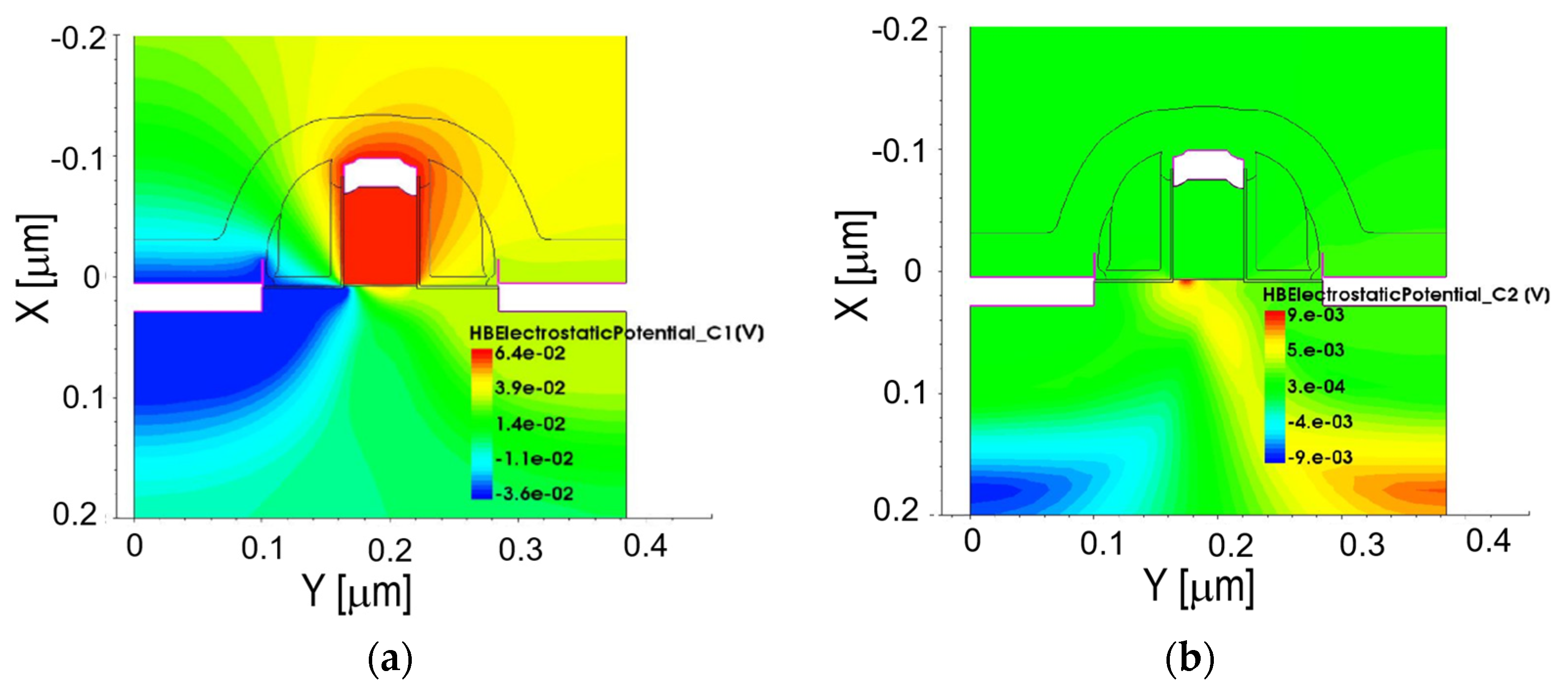
2.1. Electrostatic Potential

The predictions of the self-mixing model can be verified by studying the MOSFET response to the THz radiation by HB analysis, which allows the identification of the device regions where the nonlinear interactions responsible for the detection mechanism mainly occur. Figure 1a reports a color map of the simulated zeroth-order harmonic component of the electrostatic potential in the cross-section of an ST B55 Technology NGH MOS. The transistor is stimulated by a 0.7 THz RF signal of nominal amplitude of 100   m V , applied between the source and the gate. The source and gate–source bias of the transistor are V S = 0.5   V and V G = 0.6   V , respectively. The white areas, depicted in the color map, represent silicide high-conductivity regions not included in the simulation domain but taken into account by suitable boundary conditions. As is clearly visible in the figure, the electric field is maximum at the source oxide gate corner where the potential gradient undergoes the steepest variation. Figure 1b shows a 2D map of the second-order harmonic response of the electrostatic potential: the point in which the nonlinear interaction occurs is easily identifiable.

2.2. Self-Mixing Voltage

HB simulations can extract the rectified potential in the CMOS structure due to self-mixing. In particular, a procedure is required which subtracts the zeroth-order harmonic component from the equilibrium electrostatic potential. Figure 2 reports the 2D color maps of the self-mixing rectified potential (conventionally labeled as AA in the legends). Results refer to numerical simulations of the same structure, RF signal, and source bias as in Figure 1; panels (a), (b), and (c) correspond to V G =   0.5   V , 0.6   V , and 0.7   V , respectively.
Numerical results highlight a two-step spatial distribution of the self-mixing rectified potential: a first step occurs between the source and the channel, while a larger second step occurs between channel and drain. The origin of these distributions was explained in [31]. The first step is due to the self-mixing dipole, while the second one is due to the accumulation of electrons at the drain. As shown in Figure 2c, in the case of a higher gate voltage, when the transistor is in strong accumulation, the rectified voltage at the drain decreases. In this case, two concurring effects take place. First, the barrier between the channel and the drain regions decreases, so the potential at the drain necessary to compensate the self-mixing current also decreases. Second, the penetration of the RF potential is reduced due to the screening by the channel charge. The two effects lead to a reduction in the generated photovoltage.

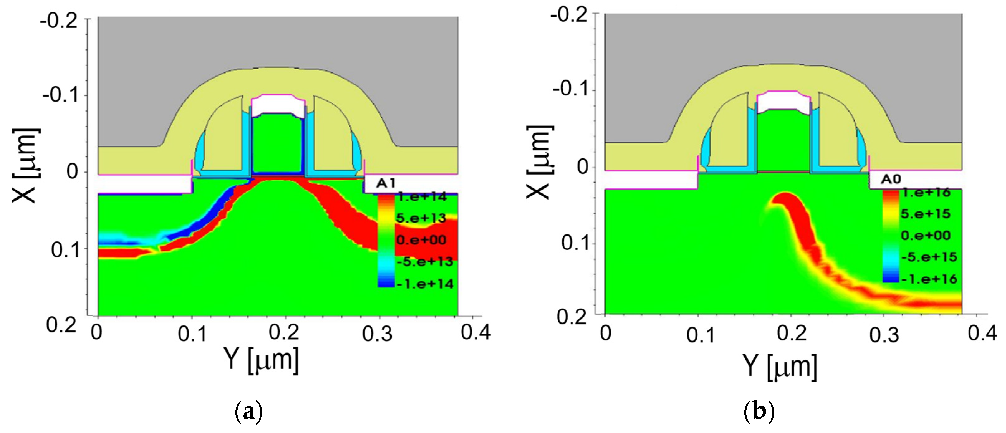
2.3. Displacements of Carriers

The carrier density variations induced by the self-mixing effect were extracted by subtracting from the HB zeroth-order harmonic solution the carrier density profile “at rest”, i.e., the steady state carrier density profile in the absence of the RF signal. Figure 3 shows the numerical results of the same structure described in Figure 1 and Figure 2. The electron density profile (conventionally labeled as A1) is mapped in Figure 3a. An intuitive representation of the physics underlying the rectification mechanism can be extracted from this figure. A variation in electron density takes place all along the junction between the doped source zone and the substrate. Nevertheless the electron density variation propagates exclusively along the channel spreading into the drain zone. At the source barrier, a dipole is generated by the self-mixing mechanism, where positive and negative variations are evident, whereas in regions close to the drain, where no RF signal is present, only a positive variation occurs. Figure 3b reports a 2D color map of the self-mixing variation of the hole density (conventionally labeled as A0) for the same structure and bias as in Figure 3a. The accumulation of holes is driven by the electron flux along the channel that charges the drain capacitance.

3. Receiver Design

The present work stems out of a collaboration with the STMicroelectronics company, in particular with the Semiconductor Technology Development group, based in Grenoble, involved in the development of a THz receiver based on the B55 technology. The B55 ST technology is particularly suitable for the realization of high-frequency transmission systems since it features an extensive series of metal layers specifically aimed at the realization of high frequency electromagnetic structures. Our design involves the use of the nMOS General Purpose High-Vt 0.060 μm transistor (referred to as NGH_0.060).
The design and optimization of an integrated MOS-based THz receiver involves the analysis of the complex interplay between the characteristics of its main components, i.e., the antenna, the detecting rectifier transistor (TR), and the Low-Noise Amplifier (LNA) transistor. A 3D schematic representation of the receiver is shown in Figure 4a. The antenna terminals are connected to the source and gate by vias passing through the circuit layers. The drain contact of the detector is connected to the gate of the first LNA transistor. In the figure, the red arrows indicate the width H and W of the gates of the TR and LNA, respectively. Figure 4b shows the receiver circuit block diagram, with the connections between the antenna, the rectifier, and the LNA, whose input capacitance is highlighted.
Accurate numerical simulations were carried out to suitably model the receiver building blocks and their coupling interactions. Then, the study focused on identifying the key degrees of freedom of the system to obtain the optimal geometry of the overall architecture. The optimization of the receiver must be pursued by a suitable choice of the value of its main free parameters, in particular H and W , which affect the value of the output resistance of the parasitic capacitances and of the noise power. The analysis, detailed in Section 2, has also shown a strong dependence on the gate–source bias V G S _ T R of the detecting transistor, which determines the electron buildup in the channel. We notice that the gate–source voltage V G S _ L N A of the LNA transistor corresponds also to the polarization potential between the detector channel and the substrate since the detecting transistor must operate at zero DC current condition. Thus, this potential also contributes to determine the electron density in the detector transistor channel due the body effect. Therefore, these two parameters must also be considered in the optimization.

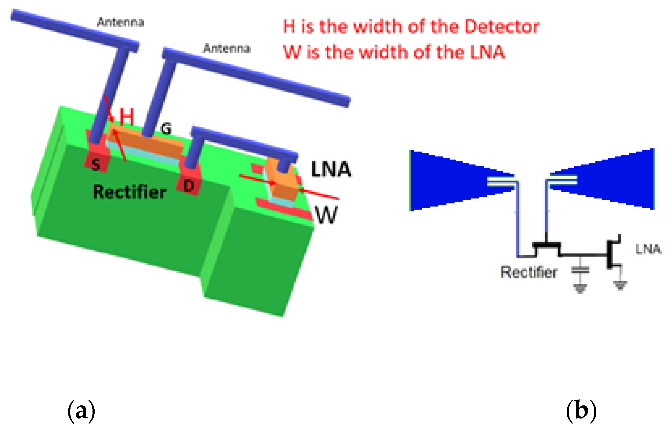
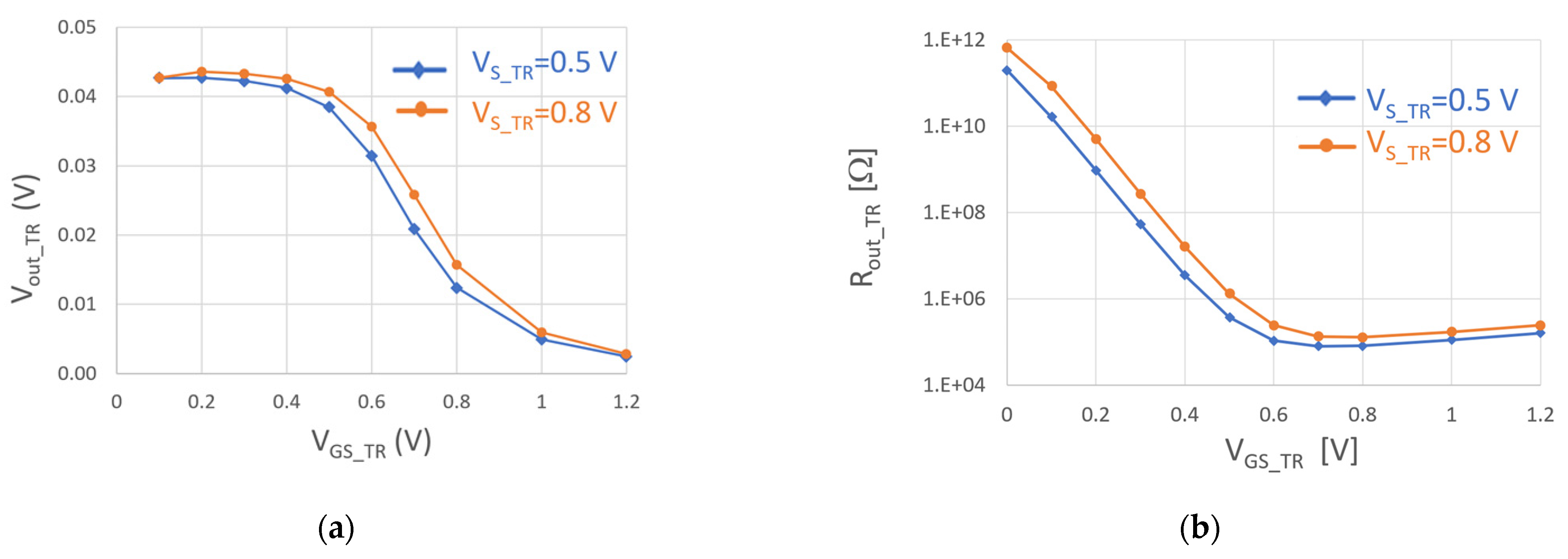
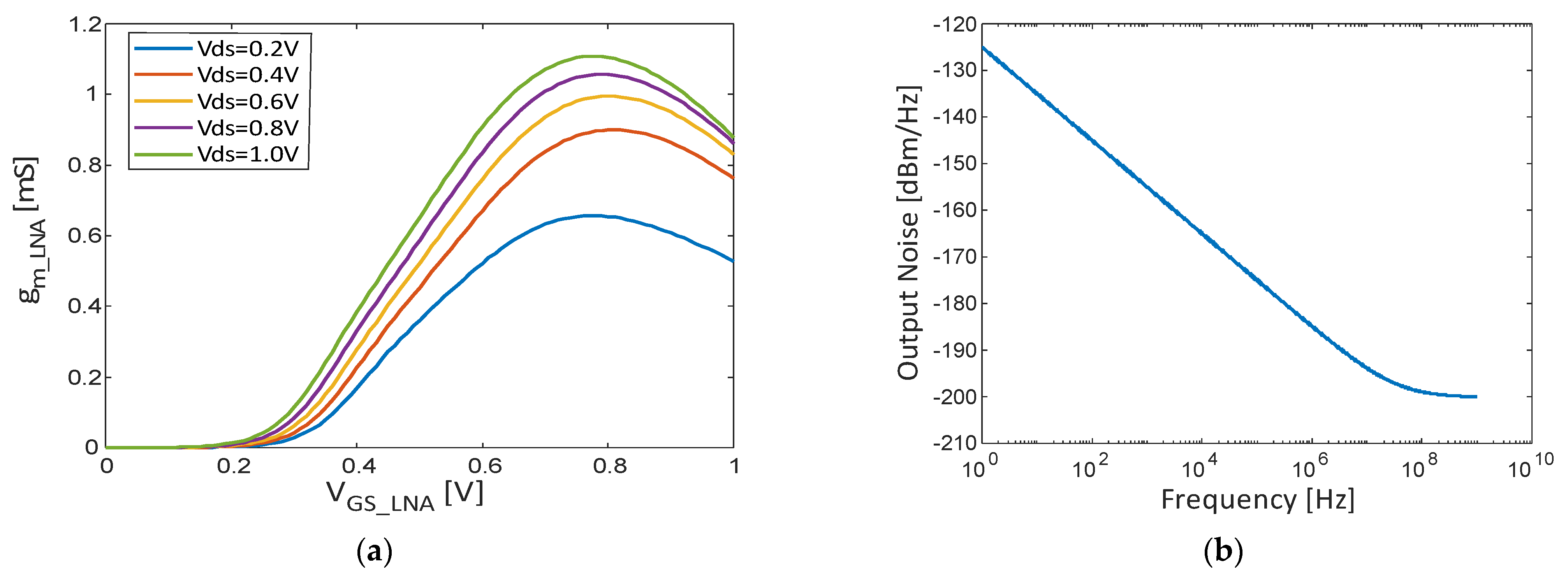
3.1. Analysis of the Detector/LNA Coupling

The values of the gate–source bias and of the geometrical width, H , of the detector transistor directly influence its high frequency impedance. A suboptimal choice of these parameters would not ensure impedance matching with the antenna inductance at resonance and would fail to grant the desired reception efficiency. Furthermore, the driving capability of the input capacitance of the LNA would be degraded.
Careful consideration must also be given to the choice of the detector source bias since it coincides with the gate–source bias of the LNA input transistor.
A suitable modeling of both the TR rectifier and LNA allows for the optimization of the width of the LNA transistor W and the evaluation of the signal to noise ratio (SNR) of the receiver. Figure 5 indicates schematically the dependence of the equivalent circuit elements on the two main optimization parameters: H and W , the widths of the TR and LNA transistors, respectively.
Figure 5a depicts the Thevenin equivalent circuit of the rectifier, where V o u t _ T R , R o u t _ T R , and C G S _ L N A denote the output voltage of the rectifier, its output resistance, and the input parasitic capacitance of the LNA, respectively. After the optimization, the TR transistor works in moderate inversion. The relatively resistive channel introduces a noise source, en_TR, which strongly contributes to the reduction in the signal-to-noise ratio. We notice that this contribution scales with the dimension of the transistor as H . The overall functional dependence on parameters H and W is highlighted in Figure 5.
In the circuit shown in Figure 5b, both the transconductance current generator and the drain noise current generator of the LNA transistor, respectively, g m _ L N A , and i n d , are represented. In particular, g m _ L N A depends linearly on W , while i n d depends on W . The larger W is, the more the LNA will contribute to increasing the signal-to-noise ratio.
The peculiarities of the specifications of the receiver and the mutual relationship between H and W influence the design. Particularly, we notice that the spectral extension of the base-band signal imposes a minimum cut-off frequency, f H . It follows that W cannot be chosen arbitrarily large since C G S _ L N A W , and thus, it contributes to limit the cut-off frequency of the receiver, f H = 1 2 π   R o u t T R C G S L N A , which must be larger than the maximum frequency of the base-band signal. This high-pass frequency comes in general from the antenna parameter and the technology of the transistor. In the case study we are presenting here, we designed a specific receiver for a system with a limited bandwidth, 100 MHz, imposed by the bandwidth of the generator available in the final experiment. We chose intentionally to reduce the bandwidth in order to reduce the overall noise. With the antenna parameters reported in the next section, and with the adopted 60 nm technology, this frequency can reach 3 GHz without a substantial limitation of the spectral distribution of the short-circuit current measured after the LNA transistor.
On the other hand, R o u t _ T R 1 / H : it can be decreased by increasing the size of the detecting transistor, though this reduces the level of the signal delivered from the antenna to the detector (as indicated by Equation (1) reported in the next Section 3.3). A suitable tradeoff must therefore be sought by jointly adjusting the values of W and H .

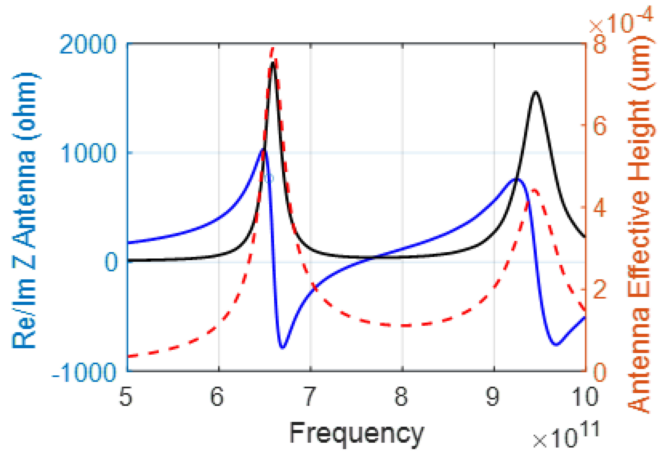
3.2. The Antenna Design

The antenna represents the most crucial component within the THz transceiver system. Typically, off-chip antennas like horn antennas [32] and mirror reflector antennas are employed. However, this approach tends to hinder the system integration, thus slowing down the commercialization process of THz technology.
This challenge has spurred significant research into on-chip antennas. Actually, CMOS technology holds the potential to enable the integration of the entire THz system onto a single chip in a cost-effective way. Recently, efforts have been made in this direction [33].
Modeling of the electromagnetic behavior of the integrated antenna and optimization of its geometrical layout has been carried out by using full-wave numerical simulations based on the Finite Integration Technique (FIT) available in the commercial software CST Studio Suite [34].
The antenna’s conductive elements are implemented in the topmost ultra-thick metallization of the eighth metal layer, available in ST B55X technology. Connections of the antenna terminals to the source and gate of the MOS TR detector are made by a suitable stacking of metal vias running through the layers of the integrated circuit back-end.
After a preliminary exploration of the parameter space of the stand-alone antenna in terms of gain, bandwidth, and impedance, its design was optimized by taking into account the constraints due to the technology design rules. The constraints related to the overall metal density of the integrated circuit, the metal densities of the single layers, and the number, distance, and thickness of the vias were evaluated by inserting dummy metal tiles and by avoiding isolated vias. This resulted in a degradation of the stand-alone antenna performance.
Figure 6 reports the parameters of one of the antennas developed during the optimization phase of the receiver. In particular, it shows the frequency behavior of the antenna-equivalent circuit, including the contribution of the vias employed to connect the antenna to the rectification device located beneath it. The black curve identifies the real part and the blue one the imaginary part of the input impedance, while the dotted red line represents the effective height of the antenna. The circle indicates the optimum working point calculated following the procedure illustrated in Section 3.4.
At the resonance frequency, the imaginary parts of the impedance of the optimized antenna and of the detector must be compensated reciprocally. The resulting resistive divider defines the reception efficiency.

3.3. Analysis of the Antenna–Rectifier Coupling

The numerical modeling of the MOS detector allows the evaluation of its high frequency (HF) response to the exciting RF signal and the assessment of the antenna–rectifier coupling. Figure 7 shows the detector impedance obtained by simulating its high-frequency response to a 0.7 THz RF signal with an amplitude equal to 100 mV. While the simulation of the antenna provides the imaginary and real part of the antenna impedance, TCAD simulations give the imaginary and real part of the TR detector. In Figure 7a,b, the detector resistance ( R s e r i e s _ T R ) and reactance ( X s e r i e s _ T R ), simulated for a 1   μ m wide TR transistor, are plotted versus the detector gate–source bias V G _ T R , assuming two different values of detector source bias V S _ T R . The latter quantity, which coincides with the gate–source bias of the LNA input transistor, is shown to moderately influence the impedance value.
At the resonance frequency, the following condition must be satisfied:
I m Z A N T + X s e r i e s _ T R H = 0
where Z A N T is the antenna series impedance and H is expressed in μm. Due to the limited range of values spanned by the imaginary part of the antenna impedance, the condition cannot be met for any value of H . The optimization has to be conditioned. The amplitude of the voltage applied at the detector is
V T R = V A N T R e Z A N T + R s e r i e s _ T R H R _ ( s e r i e s _ T R ) + j X _ ( s e r i e s _ T R ) H
where V A N T is the THz voltage, as given by the antenna effective height for a nominal incident power of 1 W/m2. The rectified potential depends on the squared amplitude of the THz voltage reaching the detector, V T R . The parameter H is thus essential to determine the ratio in Equation (1), and in turn, all the optimization process.

3.4. The Receiver Optimization

The optimization process presented in this article is a typical procedure for optimizing the signal/noise ratio of a THz receiver currently available in the literature and represents an essential step with any communication protocol.
The LNA transistor takes as input the voltage rectified by the TR transistor and performs a first amplification. The main design goal is the maximization of the signal-to-noise ratio at the LNA output. The main parameter available for this optimization is the width of the LNA input transistor, W .
The simulated output voltage V o u t _ T R and resistance R o u t _ T R of the rectifier are reported in Figure 8a and Figure 8b, respectively. The results refer to a voltage with frequency equal to 0.7 THz and amplitude equal to 100 mV applied between the gate and the source of the transistor. Furthermore, the width of the detector transistor is assumed equal to 1 μm. V o u t _ T R is assumed independent of H , while R o u t _ T R scales as 1 / H .
The gate–source capacitance of the LNA, C G S _ L N A , acts as the load of the rectifier. Its value was evaluated by Cadence simulations using the technology Process Design Kit [35]. In this case, the frequency of evaluation depends on the band of the signal in the base band. In the data reported in Figure 8, f H = 150   M H z .
The transconductance of the LNA transistor g m _ L N A as a function of the gate–source and drain–source voltages and the drain noise current i n d were also extracted from Cadence simulations. The results are reported in Figure 9a, where the transconductance g m _ L N A , is plotted versus the gate–source bias V G S _ L N A for different values of the drain–source bias V D S _ L N A . The transconductance exhibits a maximum value at V G S _ L N A 700 800   m V . The maximum value increases with V D S _ L N A . A typical value for V G S _ L N A = V D S _ L N A = 500   m V is 490   μ S .
In Figure 9b, the LNA output noise spectral density at V G S _ L N A = V D S _ L N A = 500   m V is plotted versus the signal frequency. A noise corner frequency of approximately 45   M H z is noticeable, which must be considered in the design of the receiver. It is assumed that the base-band signal spectrum extends between f L = 45 MHz and f H = 150 MHz, which corresponds to a bandwidth of approximately 100 MHz. The white noise level at a frequency of 100   M H z is 199   d B m / H z .
In addition to the considerations developed in Section 3.2, here we notice that, as shown in Figure 9b, R o u t _ T R depends on the polarization applied between the gate and source of the TR, V G _ T R . The same polarization determines the rectified voltage, V o u t _ T R . From Figure 8a, one can also note that V o u t _ T R is reduced as V G _ T R increases. There is not a univocal dependence of the detector sensitivity on the polarization, and an optimization process must be carried out, including also this parameter.
Overall, one can see how the parameters are strictly interconnected, influencing both the THz potential at the detector and the amplitude of the base-band signal.
Figure 10 reports an example of the parameter optimizations, showing the frequency dependence of the minimum power density of a plane wave impinging on the structure, as used in CST simulation, for different values of the parameter H.
The overall optimization process is quite complex and requires iterative use of different tools. We simulate by TCAD the rectifier transistor for different frequencies, values of gate–source voltage, and values of source–body voltage. The optimizer uses interpolation between the simulated points. From Cadence and from the PDK of the technology, we obtain noise values at the drain and the values of drain parasitic capacitance of the TR transistor, stored in look-up tables. The parameters of the LNA, noise, transconductance, and parasitic capacitance are also obtained from Cadence and from the B55-X technology PDK and are stored in a look-up table. Again, the optimizer uses interpolation between the simulated points. A Montecarlo procedure explores all the required values of the parameters.
The antenna is independently simulated by CST using a layout generated by Cadence.
The authors note that the method reported in this paper is the only procedure for optimizing the signal/noise ratio of a THz receiver currently present in the literature to the best of our knowledge. This optimization starts from the study of the self-mixing process in the real structure of the transistor in the chosen technology and combines these results with the technology parameters measured at low frequency and available with the PDK. The new procedure is therefore essential to optimize the receiver with any chosen antenna, MOS transistor technology, and communication protocol.

4. Conclusions

The design steps necessary to realize the CMOS THz receiver to be implemented in the B55 technology of the STMicroelectronics company have been presented and analyzed in detail. The performed investigations have highlighted that the optimization of the complete MOS-based THz receiver involves the analysis of the complex interplay between its components. Accordingly, the modeling and optimization processes require different simulation approaches. To this end, a semi-classical device simulator was used to model the nonlinear interaction of the electromagnetic field with an NGH MOSFET structure, while a compact model-based circuit simulator was adopted to model the LNA input stage. The antenna was modeled using the full-wave Finite Integration Technique (FIT). The role of the main design parameters and the tradeoffs to be handled were clearly identified and useful guidelines towards a design optimization strategy were provided. The proposed study can provide useful insights to researchers and designers of future signal receiver systems operating the THz frequencies.

Author Contributions

Conceptualization, F.P.; Methodology, F.P., R.C. and O.T.; Software, D.L. and F.C.; Resources, P.C., F.M. and A.T.; Writing—review & editing, C.S.; Funding acquisition, A.d. All authors have read and agreed to the published version of the manuscript.

Funding

This work was partially supported by the European Union under the Italian National Recovery and Resilience Plan (NRRP) of the Next Generation EU partnership on “Telecommunications of the Future” (PE00000001—program “RESTART”). This work was also partially supported by the Commission of the European Union under the HORIZON-KDT-JU grant SHIFT “Sustainable tecHnologies enablIng Future Telecommunication applications” no. 101096256.

Data Availability Statement

All data underlying the results are available as part of the article, and no additional source data are required.

Conflicts of Interest

The authors declare no conflicts of interest.

References

  1. Guerboukha, H.; Nallappan, K.; Skorobogatiy, M. Toward real-time terahertz imaging. Adv. Opt. Photonics 2018, 10, 843–938. [Google Scholar] [CrossRef]
  2. Islam, M.S.; Cordeiro, C.M.; Franco, M.A.; Sultana, J.; Cruz, A.L.; Abbott, D. Terahertz optical fibers. Opt. Express 2019, 28, 16089–16117. [Google Scholar] [CrossRef]
  3. Zaytsev, K.I.; Dolganova, I.N.; Chernomyrdin, N.V.; Katyba, G.M.; Gavdush, A.A.; Cherkasova, O.P.; Reshetov, I.V. The progress and perspectives of terahertz technology for diagnosis of neoplasms: A review. J. Opt. 2019, 22, 013001. [Google Scholar] [CrossRef]
  4. Smolyanskaya, O.A.; Chernomyrdin, N.V.; Konovko, A.A.; Zaytsev, K.I.; Ozheredov, I.A.; Cherkasova, O.P.; Coutaz, J.L. Terahertz biophotonics as a tool for studies of dielectric and spectral properties of biological tissues and liquids. Prog. Quantum Electron. 2018, 62, 1–77. [Google Scholar] [CrossRef]
  5. Yachmenev, A.E.; Lavrukhin, D.V.; Glinskiy, I.A.; Zenchenko, N.V.; Goncharov, Y.G.; Spektor, I.E.; Ponomarev, D.S. Metallic and dielectric metasurfaces in photoconductive terahertz devices: A review. Opt. Eng. 2019, 59, 061608. [Google Scholar] [CrossRef]
  6. Yachmenev, A.E.; Pushkarev, S.S.; Reznik, R.R.; Khabibullin, R.A.; Ponomarev, D.S. Arsenides-and related III-V materials-based multilayered structures for terahertz applications: Various designs and growth technology. Prog. Cryst. Growth Charact. Mater. 2020, 66, 100485. [Google Scholar] [CrossRef]
  7. Lepeshov, S.; Gorodetsky, A.; Krasnok, A.; Rafailov, E.; Belov, P. Enhancement of terahertz photoconductive antenna operation by optical nanoantennas. Laser Photonics Rev. 2017, 11, 1600199. [Google Scholar] [CrossRef]
  8. Pfeiffer, U.R.; Kutaish, A. Terahertz Light-Field Imaging with Silicon Technologies. IEEE Open J. Solid-State Circuits Soc. 2024, 4, 1–11. [Google Scholar] [CrossRef]
  9. Zatta, R.; Jagtap, V.S.; Grzyb, J.; Pfeiffer, U.R. Broadband Lens-Integrated CMOS Camera-Type THz Compact Antenna Test Range. IEEE Trans. Terahertz Sci. Technol. 2021, 11, 527–537. [Google Scholar] [CrossRef]
  10. Zhu, K.; Ding, Q.; Mao, T.; Tang, X.; Xiao, Y.; Qin, H.; Sun, H. Experimental Realization of 16-Pixel Terahertz Receiver Front-End Based on Bulk Silicon MEMS Power Divider and AlGaN/GaN HEMT Linear Detector Array. Electronics 2022, 11, 2305. [Google Scholar] [CrossRef]
  11. Boppel, S.; Lisauskas, A.; Mundt, M.; Seliuta, D.; Minkevicius, L.; Kasalynas, I.; Roskos, H.G. CMOS Integrated Antenna-Coupled Field-Effect Transistors for the Detection of Radiation From 0.2 to 4.3 THz. IEEE Trans. Microw. Theory Tech. 2012, 60, 3834–3843. [Google Scholar] [CrossRef]
  12. Ikamas, K.; Čibiraitė, D.; Lisauskas, A.; Bauer, M.; Krozer, V.; Roskos, H.G. Broadband Terahertz Power Detectors Based on 90-nm Silicon CMOS Transistors with Flat Responsivity Up to 2.2 THz. IEEE Electron Device Lett. 2018, 39, 1413–1416. [Google Scholar] [CrossRef]
  13. Shur, M.S.; Liu, X.; Ytterdal, T. Editors’ Choice—Thin Film Transistor Response in the THz Range. ECS J. Solid State Sci. Technol. 2023, 12, 035008. [Google Scholar] [CrossRef]
  14. Liu, Z.Y.; Liu, L.Y.; Yang, J.; Wu, N.J.Z. A CMOS Fully Integrated 860-GHz Terahertz Sensor. IEEE Trans. Terahertz Sci. Technol. 2017, 7, 455–465. [Google Scholar] [CrossRef]
  15. Seok, E.; Shim, D.; Mao, C.; Han, R.; Sankaran, S.; Cao, C.; Knap, W. Progress and Challenges Towards Terahertz CMOS Integrated Circuits. IEEE J. Solid-State Circuits 2010, 45, 1554–1564. [Google Scholar] [CrossRef]
  16. Marczewski, J.; Coquillat, D.; Knap, W.; Kolacinski, C.; Kopyt, P.; Kucharski, K.; Palka, N. THz detectors based on Si-CMOS technology field effect transistors–advantages, limitations and perspectives for THz imaging and spectroscopy. Opto-Electron. Rev. 2018, 26, 261–269. [Google Scholar] [CrossRef]
  17. Nahar, S.; Shafee, M.; Blin, S.; Pénarier, A.; Nouvel, P.; Coquillat, D.; Hella, M.M. Wide modulation bandwidth terahertz detection in 130 nm CMOS technology. Eur. Phys. J. Appl. Phys. 2016, 76, 20101. [Google Scholar] [CrossRef]
  18. Dyakonov, M.; Shur, M. Detection, mixing, and frequency multiplication of terahertz radiation by two-dimensional electronic fluid. IEEE Trans. Electron Devices 1996, 43, 380–387. [Google Scholar] [CrossRef]
  19. Al Hadi, R.; Sherry, H.; Grzyb, J.; Baktash, N.; Zhao, Y.; Öjefors, E.; Pfeiffer, U. A broadband 0.6 to 1 THz CMOS imaging detector with an integrated lens. In Proceedings of the IEEE MTT-S International Microwave Symposium, Baltimore, MD, USA, 5–10 June 2011; pp. 1–4. [Google Scholar]
  20. Lisauskas, A.; Pfeiffer, U.; Öjefors, E.; Bolìvar, P.H.; Glaab, D.; Roskos, H.G. Rational design of high-responsivity detectors of terahertz radiation based on distributed self-mixing in silicon field-effect transistors. J. Appl. Phys. 2009, 105, 114511. [Google Scholar] [CrossRef]
  21. Palma, F. Self-Mixing Model of Terahertz Rectification in a Metal Oxide Semiconductor Capacitance. Electronics 2020, 9, 479. [Google Scholar] [CrossRef]
  22. Synopsys®. Sentaurus™ Sentaurus Device User Manual, Version Y-2006.06. 2006. Available online: https://www.scribd.com/document/377498693/Utilities-Ug (accessed on 5 February 2024).
  23. Meng, Q.; Lin, Q.; Jing, W.; Han, F.; Zhao, M.; Jiang, Z. TCAD Simulation foe Nonresonant Terahertz Detector Based on Double-Channel GaN/AlGaN High-Electron-Mobility Transistor. IEEE Trans. Electron Devices 2018, 65, 4807–4813. [Google Scholar] [CrossRef]
  24. Hwang, H.C.; Park, K.; Park, W.; Kim, K.R. Design and Characterization of Plasmonic Terahertz Wave Detectors Based on Silicon Field-Effect Transistors. Jpn. J. Appl. Phys. 2012, 51, 06FE17. [Google Scholar] [CrossRef]
  25. Delgado Notario, J.A.; Menziani, Y.M.; Velasquez-Perez, J.E. TCAD study of sub-THz photovoltaic response of strained-Si MODFET. J. Phys. Conf. Ser. 2015, 647, 012041. [Google Scholar] [CrossRef]
  26. Velazquez, J.E.; Fobelets, K.; Gaspari, V. Study of current fluctuations in deep-submicron Si/SiGe n-channel MOSFET: Impact of relevant technological parameters on the thermal noise performance. Semicond. Sci. Technol. 2004, 19, S191–S194. [Google Scholar] [CrossRef]
  27. Cicchetti, R.; Petrarca, M.; Perticaroli, S.; Testa, O.; Palma, F. A Novel THz CMOS Chip Composed of 64 Antenna-Detectors Array toward 6G Applications. In Proceedings of the 61st FITCE International Congress Future, Rome, Italy, 29–30 September 2022; pp. 1–4. [Google Scholar]
  28. Palma, F.; Cicchetti, R.; Perticaroli, S.; Testa, O. 6G communications Push for Effective THz Sensing Technology: MOSFET Rectification Model Needs to be Refounded. In Proceedings of the 48th International Conference on Infrared, Millimeter and Terahertz Waves (IRMMW-THz), Montreal, QC, Canada, 17–22 September 2023; pp. 1–2. [Google Scholar]
  29. Kundert, K.S.; White, J.K.; Sangiovanni-Vincentelli, A.L. Steady-State Methods for Simulating Analog and Microwave Circuits; Springer Science and Business Media: New York, NY, USA, 2013; Volume 94. [Google Scholar]
  30. Palma, F. Theoretical Analysis of the Time Transient of the THz Self-Mixing Rectification Voltage in a Semiconductor Barrier. Electronics 2023, 12, 1264. [Google Scholar] [CrossRef]
  31. Palma, F. Physical Insights into THz Rectification in Metal–Oxide–Semiconductor Transistors. Electronics 2024, 13, 1192. [Google Scholar] [CrossRef]
  32. Standaert, A.; Brancato, L.; Lips, B.; Ceyssens, F.; Puers, R.; Reynaert, P. Three techniques for the fabrication of high precision, mm-sized metal components based on two-photon lithography, applied for manufacturing horn antennas for THz transceivers. J. Micromech. Microeng. 2018, 28, 035008. [Google Scholar] [CrossRef]
  33. Xu, L.-J.; Zhao, X.-K.; Bai, X. Design of on-chip antennas for THz detector and source in CMOS. IET Microw. Antennas Propag. 2023, 17, 454–466. [Google Scholar] [CrossRef]
  34. SIMULIA CST Studio Suite(R) 2019, Dassault Systèmes, Vélizy-Villacoublay, France. Available online: https://www.3ds.com/products/simulia/cst-studio-suite (accessed on 5 February 2024).
  35. Gauthier, A.; Brezza, E.; Montagné, A.; Guitard, N.; Goncalves, J.A.; Buczko, M.; Chevalier, P. Low-Noise Si/SiGe HBT for LEO Satellite User Terminals in Ku-Ka Bands. In Proceedings of the IEEE BiCMOS and Compound Semiconductor Integrated Circuits and Technology Symposium (BCICTS), Monterey, CA, USA, 16–17 October 2023; pp. 187–190. [Google Scholar]
Figure 1. (a) Two-dimensional color map of the simulated zeroth-order harmonic component of the electrostatic potential in a ST B55 Technology NGH MOS induced by a 0.7 THz signal of nominal amplitude 100   m V , applied between source and gate. The source and gate-source bias are V S = 0.5   V and V G = 0.6   V , respectively. (b) Two-dimensional color map of the simulated 2nd-order harmonic response of the electrostatic potential.
Electronics 13 03122 g001
Figure 2. Two-dimensional map of the self-mixing rectified potential for the same structure and physical parameters as in Figure 1. The three maps refer to different values of gate-source bias V G : 0.5   V (a), 0.6   V (b), 0.7   V (c). The increase in the magnitude of the potential between channel and drain is due to the different penetration of THz electric field toward the substrate depletion barrier. The penetration of the THz potential toward the substrate reduces at higher gate voltages (panel (c)) due to the screening by the channel charge.
Electronics 13 03122 g002
Figure 3. (a) Two-dimensional color map of the self-mixing-induced variation of electron density (red color: increase; blue color: decrease). (b) Two-dimensional color map of the self-mixing variation in hole density for the same structure and physical parameters as in Figure 1 and Figure 2.
Electronics 13 03122 g003
Figure 4. (a) Three-dimensional representation of the receiver providing a depiction of the antenna terminals connected to the source and gate contacts of the MOS rectifier. The drain contact of the detector is connected to the gate of the first transistor of the LNA. The width H and W of the gates, respectively, of the TR and of the LNA input transistor are highlighted. (b) Receiver circuit diagram. The parasitic capacitance at the LNA input is highlighted.
Electronics 13 03122 g004
Figure 5. (a) Thevenin equivalent circuit or the rectifier highlighting the dependence from parameter W of the parasitic capacitance C G S _ L N A of the LNA input transistor; (b) Norton equivalent current sources of the LNA, highlighting the functional dependence on W of the LNA signal, of the transconductance g m _ L N A , and the functional dependence W of the equivalent noise current source i n d .
Electronics 13 03122 g005
Figure 6. Equivalent antenna parameters vs. frequency. Real (black) and imaginary (blue) parts of the antenna input impedance and (red dashed) antenna effective height. The circle indicates the optimum working point.
Electronics 13 03122 g006
Figure 7. Simulated resistance (a) and reactance (b) of the MOS receiver versus values of its gate–source bias, V G _ T R , for two different values of the receiver source bias, V S _ T R = 0.5   V and V S _ T R = 0.8   V . Simulations refer to the high-frequency response of the receiver to a 0.7 THz.
Electronics 13 03122 g007
Figure 8. Rectifier output voltage V o u t _ T R (a) and output resistance R o u t _ T R . (b) V G _ T R for two different values of V S _ T R .
Electronics 13 03122 g008
Figure 9. (a) LNA transconductance g m _ L N A versus the LNA gate-source bias V G S _ L N A for different values of the LNA drain-source bias V D S _ L N A . (b) LNA output noise spectral density versus the signal frequency. The noise corner frequency of 45   M H z is noticeable.
Electronics 13 03122 g009
Figure 10. Minimum power density of a plane wave impinging on the structure vs. frequency for different values of the parameter H.
Electronics 13 03122 g010
Disclaimer/Publisher’s Note: The statements, opinions and data contained in all publications are solely those of the individual author(s) and contributor(s) and not of MDPI and/or the editor(s). MDPI and/or the editor(s) disclaim responsibility for any injury to people or property resulting from any ideas, methods, instructions or products referred to in the content.

