Abstract
In this paper, the operational verification of the stacked transistor configuration is provided, focusing on the use of GaN transistors. The methodology is based on simulated and laboratory experiments. The stacked transistor configuration appears to be a promising solution to increase the voltage-blocking capability of GaN technology for high-voltage operations. Currently available GaN transistors are manufactured for 650 V of blocking voltage. Devices with a higher voltage-blocking capability are not currently available. Therefore, the stacked module was verified, while the main focus was on the driving circuit design, verification, and testing. For this purpose, two alternatives of GaN transistor technology have been compared. The main goal was to reach 800 V of blocking voltage with acceptable voltage deviation for nominal power of a power semiconductor converter.
1. Introduction
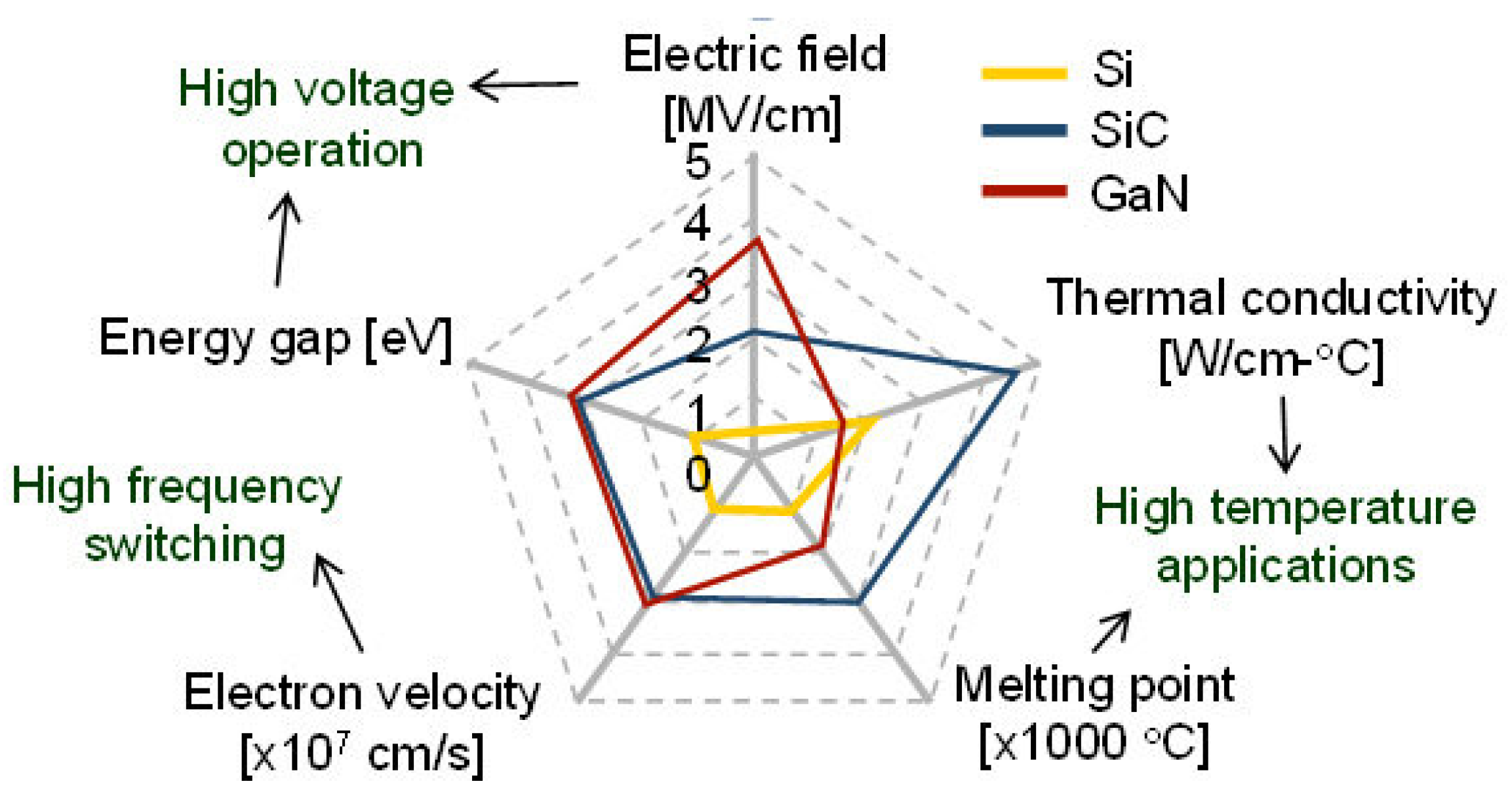
The WBG (wide bandgap) structure compared to the classical one is characterized by the width of the bandgap. This is significantly larger than one electron volt (eV). Materials with a wide bandgap compared to Si-based semiconductor wafers with a “narrow” band have several characteristics that make them attractive for use in switched mode power supplies. In principle, a comparison of the operational properties can be seen in Figure 1, provided as a simple summarization, while key performance factors are as follows:
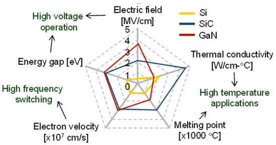
Figure 1.
Summary of the key material properties of semiconductors: Si, SiC, and GaN.
- Energy gap;
- Electric field;
- Thermal conductivity;
- Melting point;
- Electron velocity.
These differences in key parameters allow WBG elements to operate at much higher voltages than Si, switching frequencies and temperatures [1,2,3,4,5].
The basic parameters that favor SiC over Si are as follows: thermal conductivity, the size of the electric field, and the wide width of the restricted zone. The low anisotropic compatibility of 4H-SiC electrons is the main reason for the higher popularity of 4H-SiC. The high value of the width of the energy gap and the low intrinsic concentration of carriers allow SiC to operate at a very high temperature. The intrinsic concentration of carriers is directly proportional to the Nc (concentration of carriers) and Nv (concentration of holes) that occur in the conductivity and valence bands. However, as a result of the thermal expansion of the grid and of the fasteners (so-called quasi-particles propagating vibrational quantum waves in the crystal grid), this concentration has an exponential temperature characteristic (as well as the width of the prohibited energy band).
The concentration of intrinsic carriers is therefore an important parameter of a semiconductor, because the leakage current in semiconductors is directly proportional to these numbers. SiC has only a negligible amount of intrinsic carrier concentration in a given temperature range, so the conductivity is influenced by impurities. As the temperature increases, the intrinsic carrier concentration increases exponentially. The leakage current increases inadequately at high temperatures when the conductivity becomes uncontrollable, which is manifested by the excess of the doped impurity by its own charge carriers. Depending on the design of the specific component of the internal concentration of silicon carriers, the operation of the SiC semiconductor junction is limited to less than 300 °C. A much smaller intrinsic concentration of SiC carriers would enable operation at extreme transition temperatures, theoretically exceeding 800 °C, while the experimentally verified temperature was 600 °C [6,7,8]. Currently, it is impossible to operate the transistor at such temperatures due to the technological limitations of the package technology. Polymer cases and soldering methods are intended only for “low” temperatures. LTCC (Low-Temperature Co-fired Ceramic) cases are considered promising components for storing SiC chips. However, LTCC cases can drastically degrade driving capabilities compared to current parts. Applications for very high temperatures will therefore have to wait until suitable housings are developed [9,10,11,12,13,14,15].
The high breakdown electric field and high thermal conductivity of SiC, together with high operating temperatures, enables semiconductors to operate with extremely high energy density. If we compare the high breakdown voltage of SiC with Si, then at the same reverse blocking voltage, the SiC part will be about 10 times thinner and 10 times more doped. This fact is reflected within about a 100-fold reduction in the resistance of the blocking region, and a 100-fold reduction in the chip’s length. The high breakdown voltage and the width of SiC’s energy bandgap enable the production of extremely fast power components. Therefore, power converters using SiC-based components can work in areas of high switching frequencies with simultaneously higher efficiency (smaller switching losses). The use of high switching frequencies in converters is very desirable because it allows the use of smaller values of capacitances, inductances, and transformers, which ultimately reduce the overall dimensions and weight of the equipment [16,17,18].
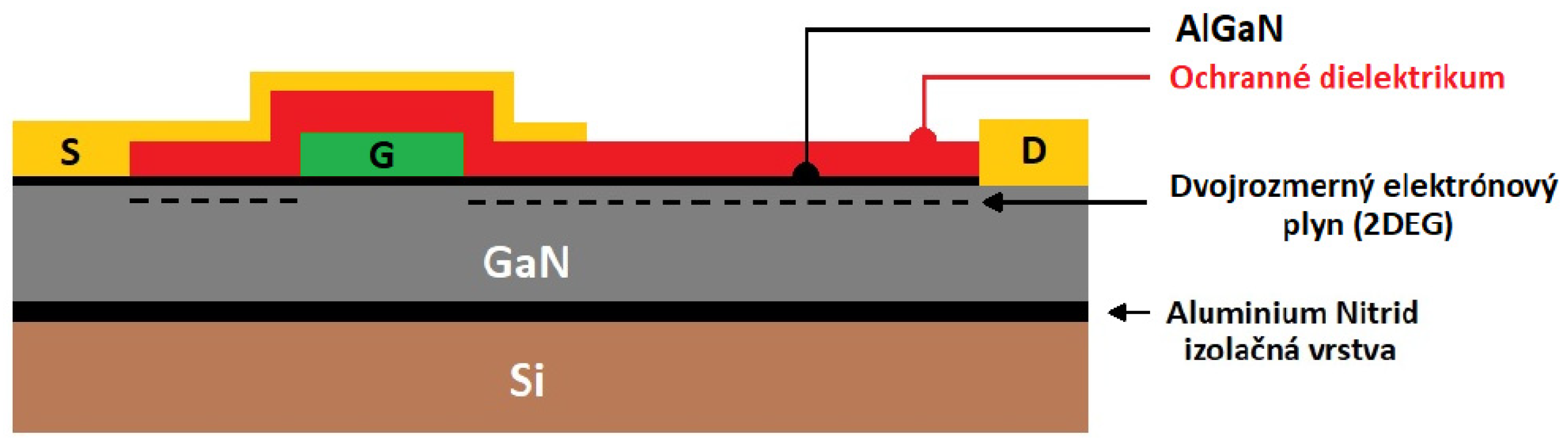
Under nominal operating conditions, GaN transistors are characterized by a very high velocity of charge carriers. Also, compared to silicon transistors, they have lower values of input capacitance CISS, output capacitance COSS, and Miller capacitance CRSS. GaN-based transistors are particularly advantageous due to the low value of resistance RDS(on), the possibility to work with high switching frequencies ranging up to units of MHz, and the reduction in switching losses, thus guaranteeing a higher overall system efficiency. The basis for production is the substrate, which can be made of silicon (Si) or silicon carbide (SiC) material. It is the thickest layer, which ensures better heat spread and heat dissipation, and mechanical support of the structure itself. In most cases, an insulating layer made of aluminum nitride (AlN) is used to insulate the structure of the device and the substrate. The GaN layer, which has a high resistivity, follows upward. The transistor´s conductivity is based on the piezoelectric phenomenon, because AlGaN is applied to the GaN layer, which creates a physical voltage. Because of the fact that GaN is a piezoelectric material, the voltage attracts electrons to the interface formed by the GaN and AlGaN layers. This concentration of electrons that have high mobility and conductivity is called a two-dimensional electron gas (2DEG). At the end, gate, drain, and source electrodes are added by various processes [2]. Different structures divide GaN transistors into two groups. In the first group, GaN transistors work in depletion mode, where their basic structure is shown in Figure 2, and the second group operates at the so-called enhancement mode, as shown in Figure 3.
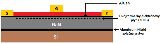
Figure 2.
Internal structure of a GaN transistor operating in depletion mode.

Figure 3.
Internal structure of a GaN transistor operating in enhancement mode.
GaN transistors are widely used in many applications, whether they are low-voltage applications up to 100 V or medium-voltage applications up to 650 V. This voltage level is a limit, meaning there is a lack of GaN power transistors suitable for applications where the nominal operating voltage is 800 V and higher (new e-mobility automotive standards on traction systems or photovoltaics applications). Until today, manufacturers have not yet been able to technologically modify the structure in such a way that it can reliably block the required voltage without affecting its excellent properties. The 800 V applications are associated with the use of higher voltages for certain electrical systems and technologies. Here are some examples where 800 V is expected to be standardized:
- Electromobility: 800 V is often used in electric cars of the latest generation. This higher voltage enables the faster charging of batteries and increases the performance of electric motors. Electric cars with a voltage of 800 V tend to achieve higher efficiency and performance, which ensures longer ranges and shorter charging times.
- High-power electric drive systems: 800 V applications are also used in high-power electric drive systems such as electric racing cars, high-speed trains, and so on. This voltage provides enough energy to drive these powerful vehicles.
- Alternative energy sources: Some alternative energy sources, such as solar and wind power plants, can also use 800 V. This higher voltage allows for more efficient transmission and distribution of the produced current into the electrical networks.
- High-performance server farms: 800 V is used in some cases in the field of IT and data centers. This higher voltage allows for increased efficiency and lower energy losses when operating powerful server systems and devices.
- Experimental and research applications: In some experimental and research areas, 800 V can be used to explore new technologies, perform tests, and verify concepts in the field of electricity and energy.
This paper focuses on the research of the possibilities to design a GaN power transistor suitable for operation at voltages exceeding the value of 650 V. One of the ways to achieve this aim is to use a series connection of transistors (stacked configuration), thus achieving a higher blocking voltage (2 × 650 V = 1300 V). For this purpose, it is very important to select suitable types of GaN transistor-aiming parameters for this application. Since the market is still “young” within this area, it was decided that two different transistors with different internal structures would be selected. As will be seen, another important facet is the configuration of the driving circuit, so research work was also focused on the circuit configuration of the driving circuit, aiming for the optimal operational conditions.
2. Selection of GaN Power Transistor Technology
We paid attention to applications with a higher operational voltage (800 V) and therefore, for testing purposes, it was necessary to consider transistors with a blocking voltage value higher than 1000 V (considering a 20% safety margin). Once SiC technology was considered, it was not a problem to choose from available transistors on the market that had components with the required blocking voltage. However, it was already a challenge to find transistors with an appropriate GaN structure, because there is not yet a GaN transistor with a blocking capability more than 1000 V on the market. Commercially produced devices are characterized with a maximum of 650 V.
The first choice of device is from GaN Systems, which is only engaged in the production and sale of GaN transistors with their own special improved e-HEMT (high-electron mobility transistor) structure. Their portfolio includes transistors with blocking voltages from 100 V/38 A, 90 A up to 650 V/4 A–150 A. They have patented Island Technology® and GaNPX® housing (Figure 4). The GANPX® package is carefully designed, exhibiting an extremely low inductance of the source electrode, which makes it possible to fully utilize the potential of the GaN e-HEMT transistor, even at very high switching frequencies. The GANPX® housing allows the transistor to be operated in the high frequency region with minimal oscillations and EMI interference [6].
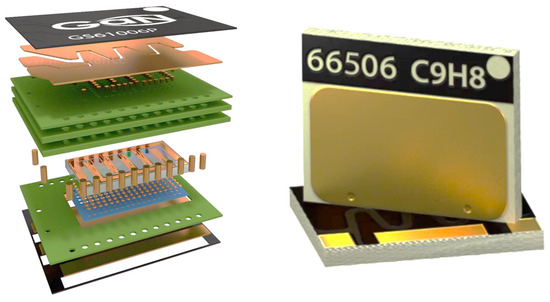
Figure 4.
(Left) Individual layers of the internal structure of the GaN Systems transistor, (Right) GANPX package.
Another advantage of GANPX® is that it allows us to use different methods for thermal management. For example, with the so-called “TOP COOLING” (cooling from the top side of the component) method, it is possible to use a low-profile heatsink, which ultimately reduces the size of the system and its cost. The second method is “BOTTOM COOLING” (cooling from the bottom side of the component), where the device is cooled through the thermal management of the printed circuit board.
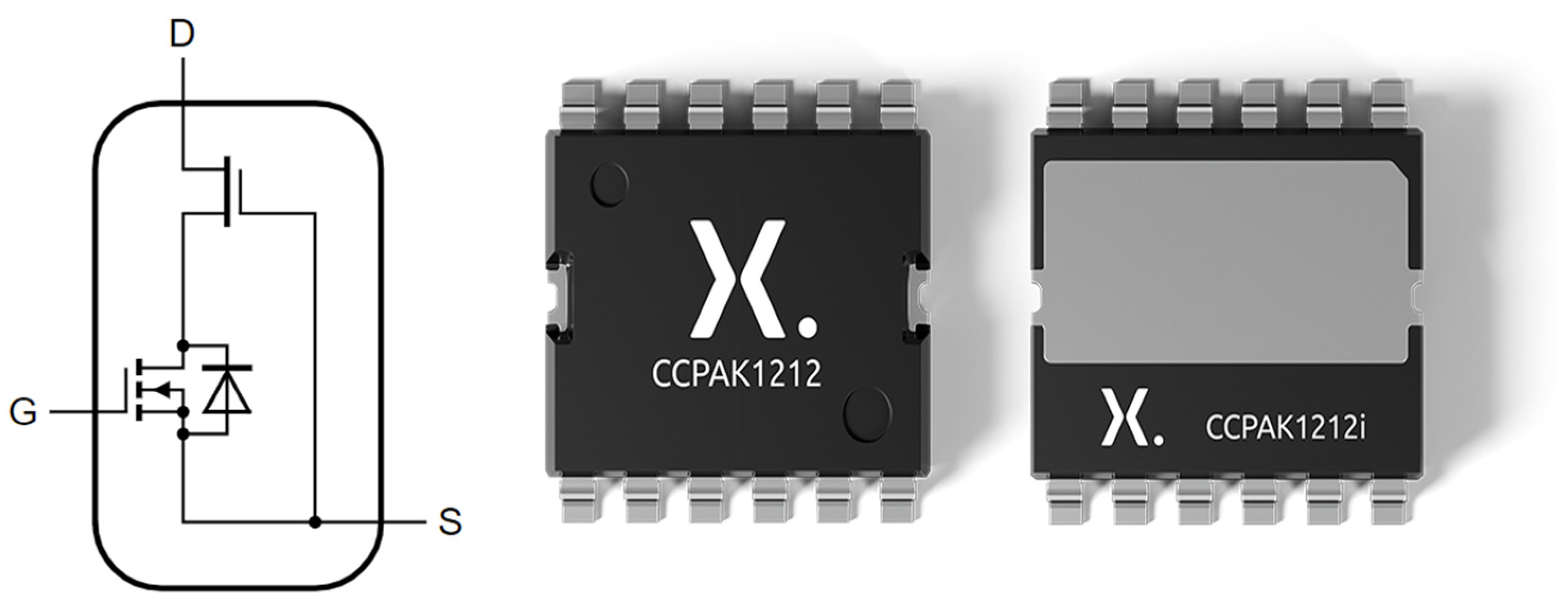
The second GaN transistor alternative has a cascode internal structure and is made by NeXperia. The GAN039-650NBB transistor consists of two transistors—the gate formed by a MOSFET structure (Si MOSFET with a low RDS(on)) and the drain–source power part formed by a GaN structure (Figure 5). As in the case of previous transistors, the manufacturer offers various methods for thermal management design.
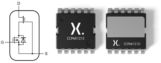
Figure 5.
GaN transistor from NeXperia in CCPAK package.
3. Investigation of the Driving Configuration Properties: Simulation Analyses
As mentioned earlier, commercially available GaN transistors do not meet a blocking voltage capability above 650 V [19,20,21]. Therefore, a high voltage GaN module was designed (Figure 6). The main goal was to benefit from the excellent properties of GaN technology, which are as follows:
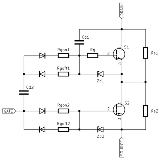
Figure 6.
Stacked configuration of the investigated high-voltage GaN module.
- Low losses;
- High efficiency;
- The possibility of operation at high switching frequencies.
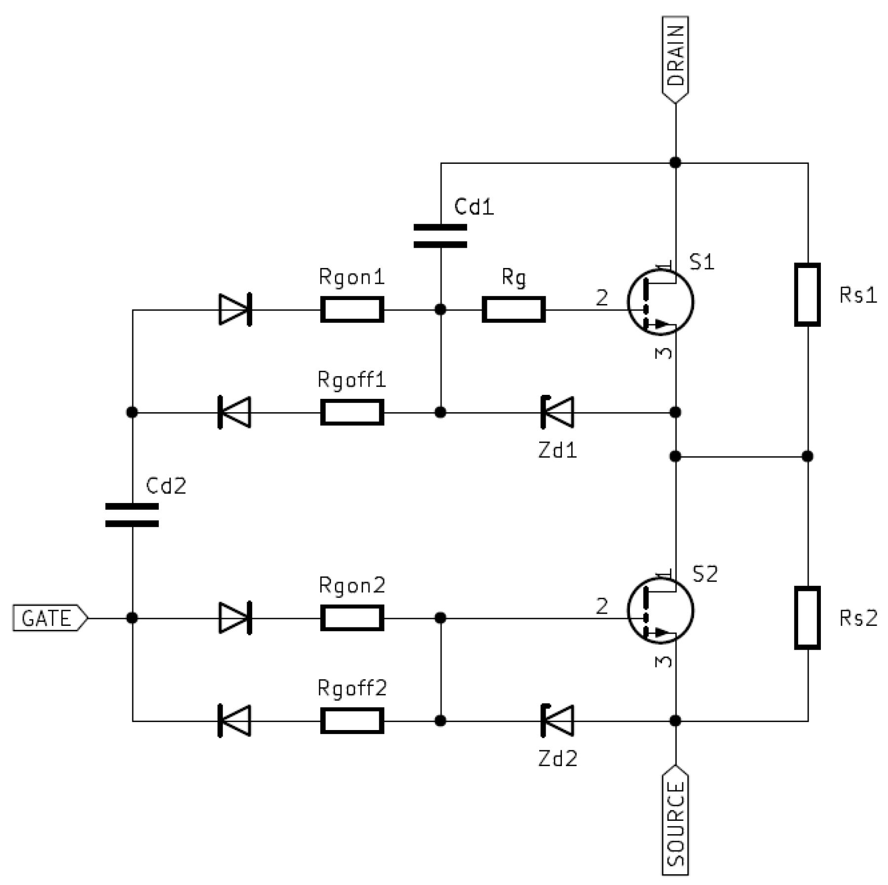
The module consists of two series-connected GaN transistors and a SSD drive circuit (Figure 6). An external drive signal was applied to the gate, which directly drove the lower transistor, while the integrated auxiliary serial drive circuit (SSD) was responsible for driving the upper transistor. The configuration of the driving circuit components was already presented and analyzed in detail in [22,23]; however, during the experimental investigation, it was found that the driving circuit can be reconfigured to provide better operational characteristics (voltage deviation on the transistors). This issue will be discussed within this paper in more detail.
3.1. Simulation of the Functionality of the HV Stacked GaN Transistor Module
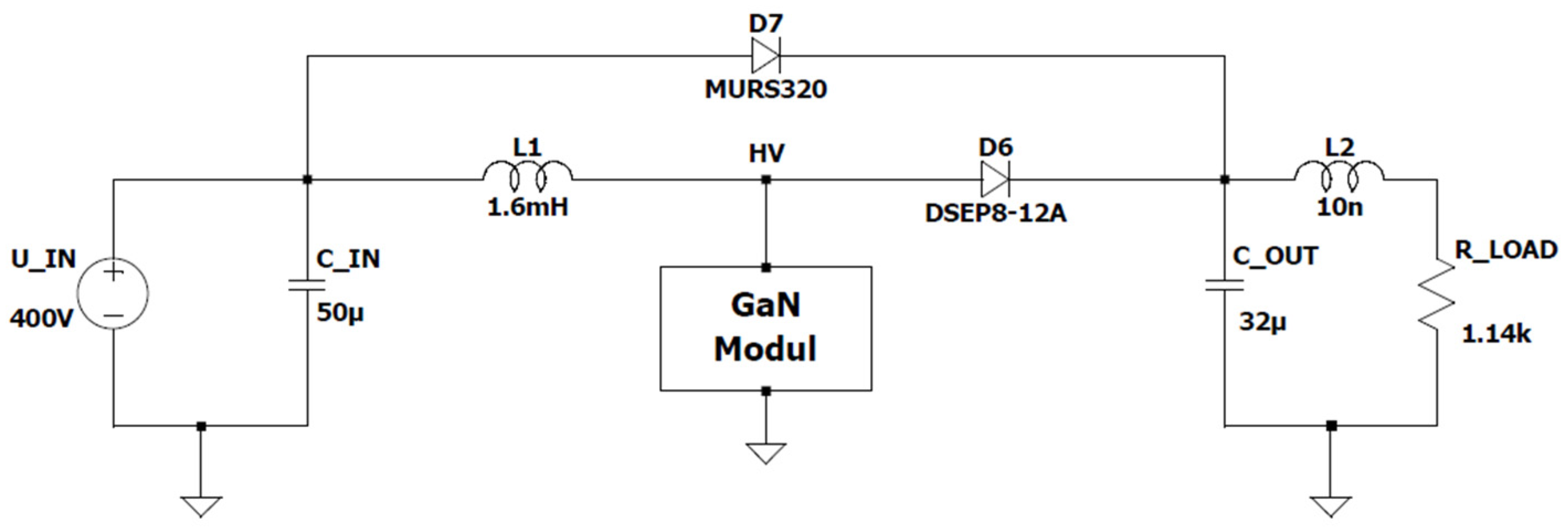
When connecting transistors in series, it is necessary to pay attention to the driving circuit design following the voltage distribution across both transistors during the blocking interval. The transistors must be driven at the same time and without significant delays so that there is no phenomenon when one of the transistors begins to block higher voltage VDS. The simulation analysis of the driving configuration of the GaN module was performed using the power circuit configuration shown in Figure 7. It represents the topology of the boost converter. Parameters of the simulation circuit are as follows:
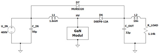
Figure 7.
Power circuit for simulation analysis of the driving configuration performance.
- Input voltage: 100 V–400 V;
- Output voltage: 200 V–800 V;
- Output power: max 600 W (the load was constantly set to RLoad = 1.14 kΩ);
- Switching frequency: 100 kHz;
- Duty cycle: D = 0.5.
In this part, attention was paid to the analysis and synthesis of different configurations of the driving circuit. The analyses were supported by simulation experiments using LTSpice software. For the evaluation of the functional behavior, a simulation model of GaN transistor GS66506 was utilized.
3.1.1. Simulation of Unipolar Driving Functionality (0 V/5 V): GaN Module Driving_v1
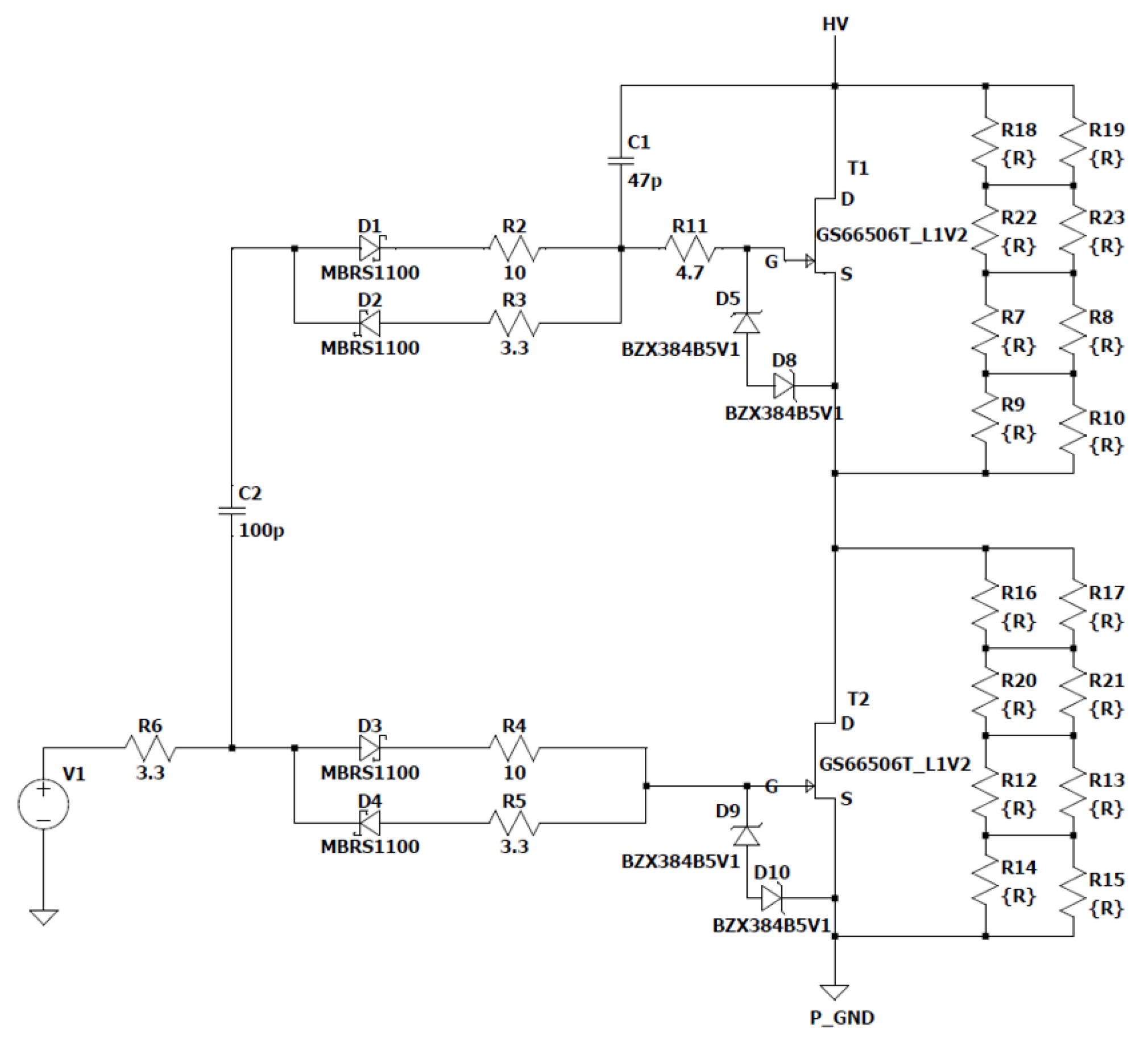
The first configuration of the driving circuit was based on the unipolar driving function. The maximum recommended gate voltage for the selected transistor was within the range −10 V ÷ 7 V. For this case, the following values were utilized: 5 V for turning on and 0 V for turning off the transistor.
In Figure 8, you can see the simulation circuit of the GaN module driving_v1, where the source V1 represents the gate signal generator, and C2 and C1 are the driving capacitors which secure the driving of the upper transistor T1. Also, for an optimal turn-on and -off process, turn-on resistances R2 and R4, and turn-off resistances R3 and R5 were added to improve the dynamics and stability of the commutation processes. Zener diodes (D5, D8, D9, D10) were used to protect the gates of the transistors.
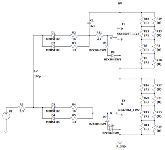
Figure 8.
Simulation model of the unipolar driving of stacked configuration GaN module.
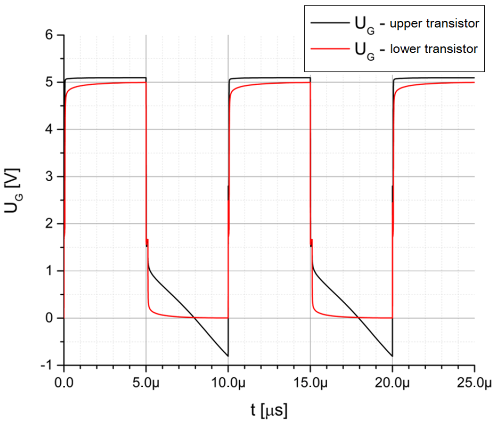
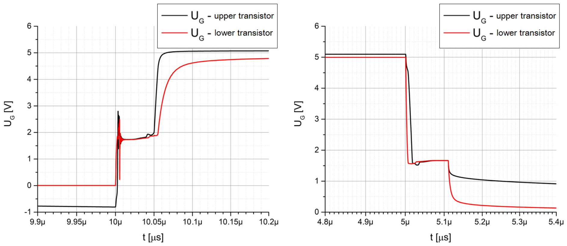
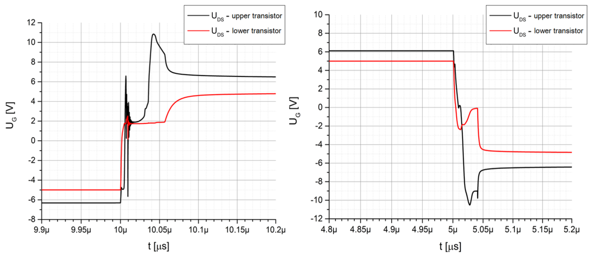
In Figure 9, you can see the simulation result, where the waveforms represent the driving signals on the gates of the transistors. The red curve represents the signal at the input to the gate of the lower transistor with a voltage level of 0 V to 5 V. However, as can be seen, the waveform of the gate signal for the upper transistor drops to −0.7 V during the turn-off sequence, which is the consequence of the voltage drop of the Zener diode.
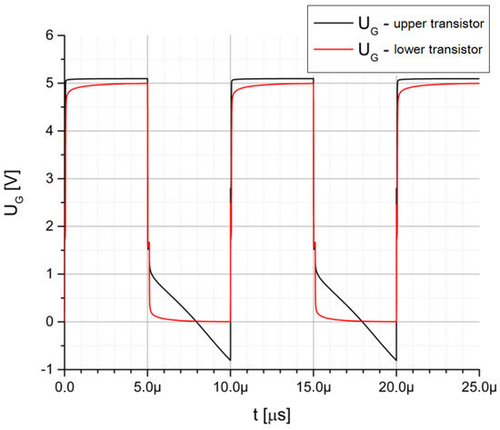
Figure 9.
Simulation results for GaN module driving_v1—waveforms of gate–source voltage.
Figure 10 presents a detailed view of the waveforms of the gate–source voltage during the turn-on and turn-off process. The total time for the turn-on process to reach a steady voltage value takes 100 ns. It is seen that once the value of Uth is reached (1.5 V–Miller plateau), the Miller capacitor starts to charge within 10 ns. At this time, the transistor is in a conductive state and begins to conduct current. During the turn-off process, it is seen again that once the value of Uth is reached, it takes another 100 ns until all the charge is removed from the gate so that the transistor goes into the closed state.

Figure 10.
Simulation results for GaN module driving_v1—details of the gate–source voltage during turn-on (left) and turn-off (right) process.
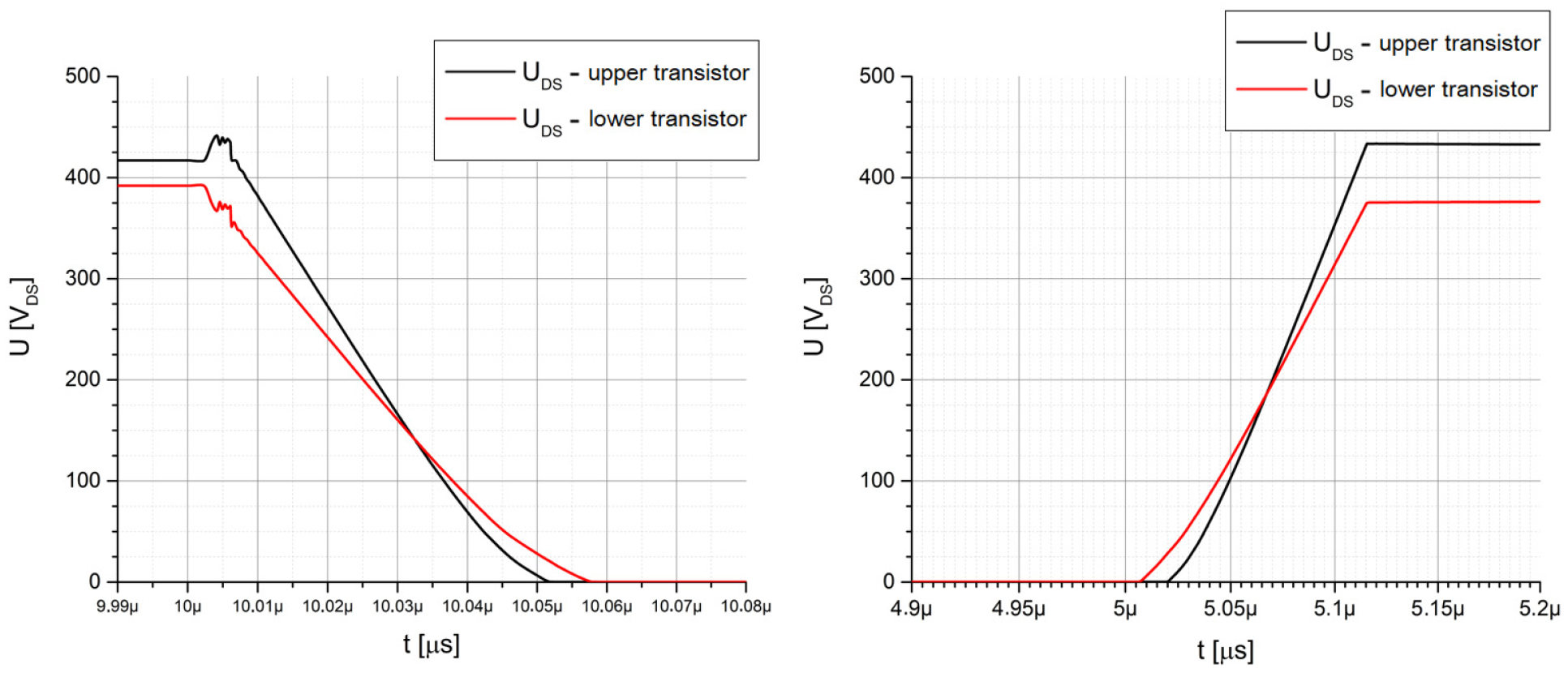
Figure 11 shows the details of the turn-on and turn-off process with the plotted waveforms of the drain–source voltage. The drain–source voltage (UDSlow) of the lower transistor starts to drop. However, the commutation process is not yet completed, which means that the entire DC voltage of the intermediate circuit is redistributed between the GaN module transistors (UDS = UDShigh + UDSlow). It is seen in Figure 11 (left) that the decrease of UDS2 leads to an increase in the voltage of UDShigh. In addition, this decrease will also cause an increase in the UG of the upper transistor during this interval (Figure 10).
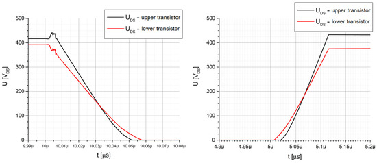
Figure 11.
Simulation results GaN module driving_v1—details of the drain–source voltage during turn-on (left) and turn-off (right) process.
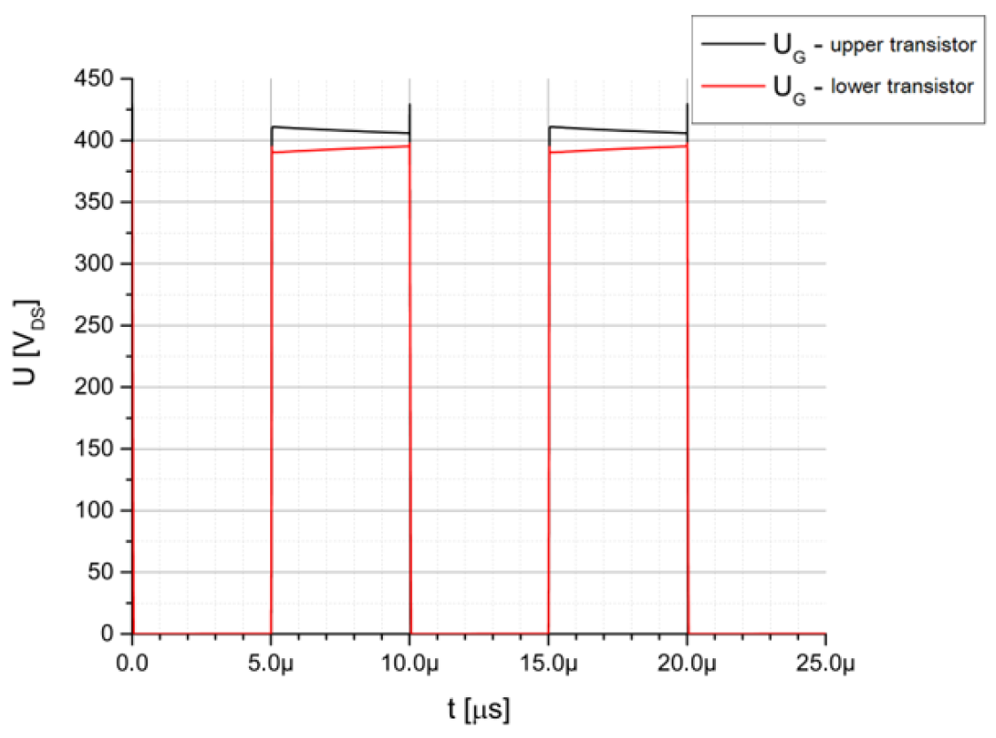
According to the optimal switching conditions, it is required that both voltages (upper and lower transistor) on the drain–source electrodes reach their maximal value almost at the same time. Another requirement considering the optimal switching conditions is that the upper transistor should have a faster turn-off process in comparison to the lower transistor. This may provide a more even distribution of the DC-link voltage within the GaN module. In Figure 12, the simulation result is referring to the time waveforms of the drain–source voltages of both transistors in the stacked configuration GaN module.
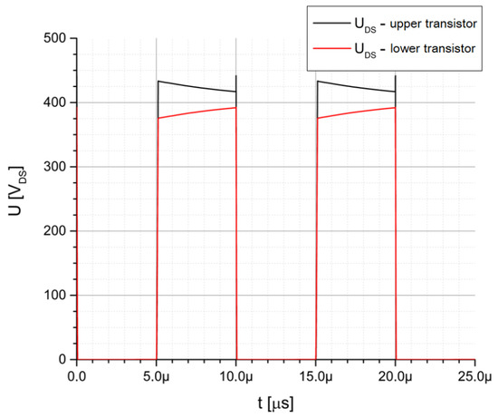
Figure 12.
Simulation results for GaN module driving_v1—waveforms of drain–source voltage during switching sequence.
By analyzing these waveforms, it was found that the redistribution of DC-link voltage between individual transistors is at the level of 15%. Summarizing these results, it can be expertly assessed that under the given operational conditions, the adverse condition of uneven voltage redistribution of the power circuit will not apply, which will not cause damage to the GaN module using the v_1 configuration of the driving circuit.
3.1.2. Simulation of Low-Side Driving (−5 V/+5 V): GaN Module_v2
Like the previous case, a simulation of another possibility of driving of the stacked GaN module was provided. Here, it is considered with a negative voltage applied to the gate of the transistor during the turn-off process. In this way, it is expected that the dynamics when the transistor is turned off should be improved. Parameters of the simulation circuit are similar to the previous case (Section 3.1), while the only change was reflected withing the driving voltage, which was set to −5 V (turning off) to +5 V (turning on). The simulation circuit is therefore the same as shown in Figure 8.
In Figure 13, the waveforms of the gate signals of the transistors are interpreted. The red waveform represents the gate signal of the lower transistor, and the waveform is exactly within the −5 V/5 V range. The black waveform represents the voltage signal on the gate of the upper transistor, which is within the limits of −6 V/6 V. This is a consequence of the voltage drop of the Zener diodes.

Figure 13.
Simulation results for GaN module driving_v2—waveforms of gate–source voltage.
The waveforms in Figure 14 present detailed switching transitions during the turn-on (left) and turn-off process (right). The waveforms are very similar in nature to the previous case (driving_v1), but with the difference that they have higher switching dynamics. A significant difference in the switching dynamics is that this type of driving manifests itself during switching off. In the previous case (Figure 11), the component is brought to the turn-off state (UG < Uth) at time 5.2 µs. In the case of driving the GaN using the driving_v2 configuration, the turn-off is significantly faster (at 5.01 µs, the transistor is turned off). Such acceleration is a consequence of the negative driving voltage application.
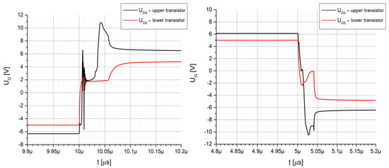
Figure 14.
Simulation results for GaN module driving_v2—details of the gate–source voltage during turn-on (left) and turn-off (right) process.
Figure 15 presents voltage waveforms between drain–source terminals. The same switching theory applies here as in the previous case. However, it can be seen that the turn-off process is faster in comparison to driving_v1. Regarding dynamics resulting in the reduction in the stitching losses, the result is appreciated. On the other hand, the demands related to protections against interference and unwanted switching of transistors are required, since in this case, a high dv/dt will be achieved.
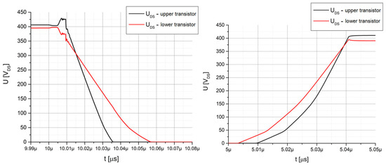
Figure 15.
Simulation results for GaN module driving_v2—details of the drain–source voltage during turn-on (left) and turn-off (right) process.
Figure 16 shows the switching sequence for GaN module driving_v2 with the drain–source voltage of the module. From the results, it is seen that the redistribution of DC-link voltage between the individual transistors is lower compared to the results obtained from the driving_v1 configuration (Figure 12). It is therefore expected that symmetrical bipolar driving signals would provide better performance during the operation of the stacked GaN module.
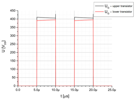
Figure 16.
Simulation results for GaN module driving_v2—waveforms of drain–source voltage during switching sequence.
3.1.3. Simulation of Pulsed Transformer Driver: GaN Module_v3
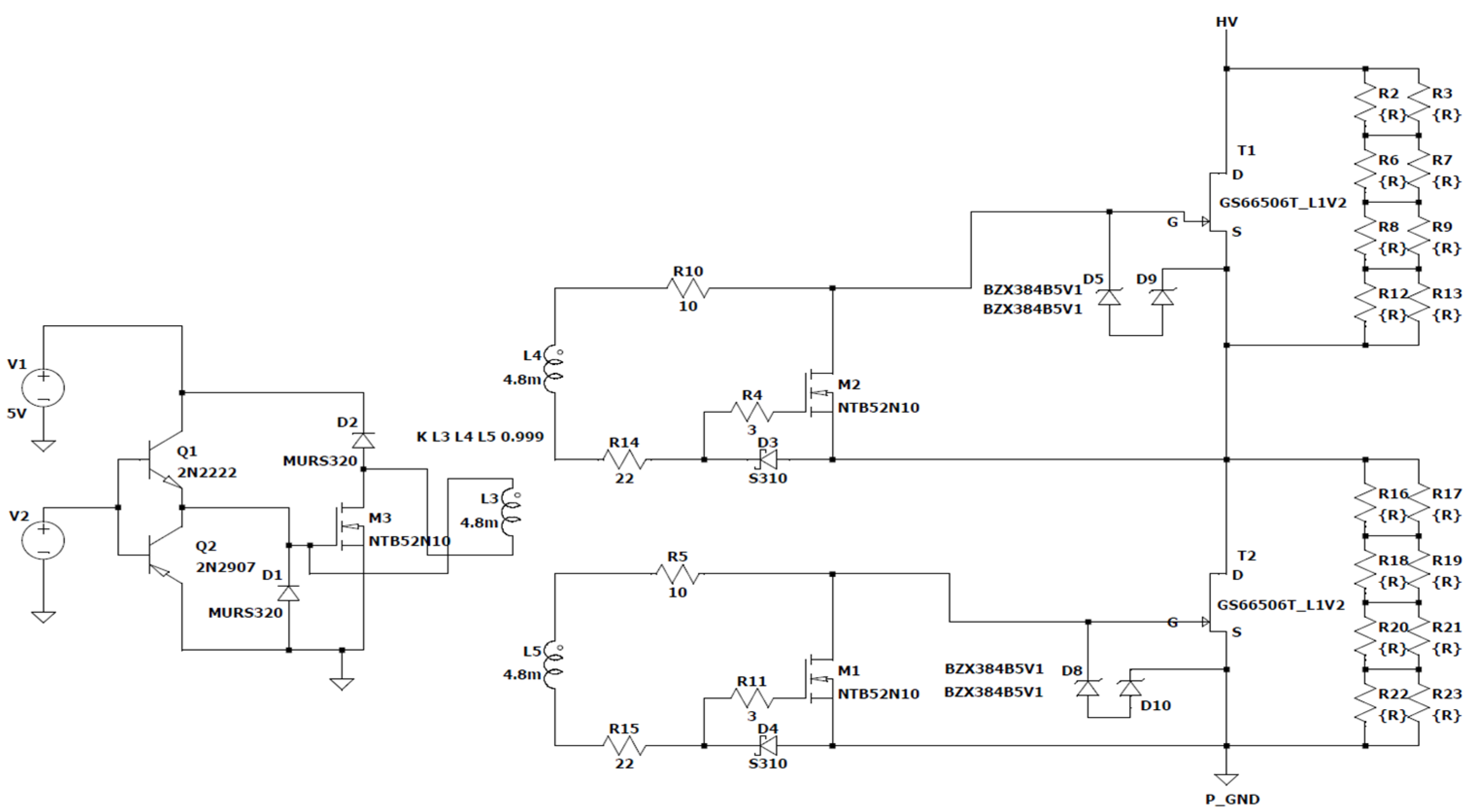
Another option for driving circuit design is a pulsed transformer driving circuit, which ensures the isolation of driving signals to both transistors at the same time. In Figure 17, the circuit diagram is shown, where the primary side represents the driving circuit of the transformer, which consists of the “totem-pole” transistor configuration (Q1-NPN and Q2-PNP transistors) and the demagnetization circuit of the transformer (D4, D6, and M3). On the secondary side, a circuit composed of N-channel MOSFET transistors (M1, M2) and diodes (D3, D4) is visible. Circuit parameters are the same as described in Section 3.1. The driving voltage in this situation ranges from 0 V to 5 V.
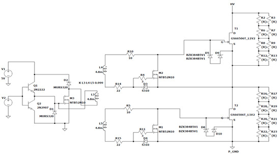
Figure 17.
Simulation model of the pulsed transformer driving of stacked configuration of GaN module.
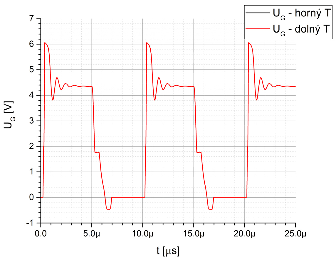
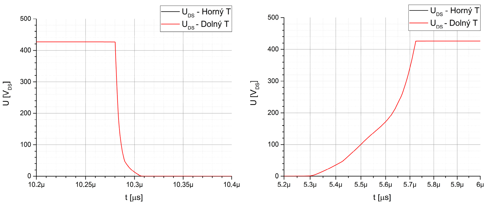
In Figure 18, the waveforms of gate–source voltages are shown. It is seen that these waveforms overlap one another, and this condition represents an ideal situation according to the stacked configuration driving. In this way, it is expected that none of the power transistors in the stacked configuration will sustain the full DC-link voltage, not even for a short period.

Figure 18.
Simulation results for GaN module driving_v3—waveforms of gate–source voltage.
Figure 19 shows the details of the turn-on and turn-off process according to the gate–source voltages. Comparing to the previous methods of driver design, the transition of these intervals is 10 nanoseconds slower. On the other hand, the pros of this fact includes the dv/dt reduction, which represents a critical parameter during transistor switching. This is reflected within the waveform of the UDS (Figure 19), while the rise/fall is significantly slower compared to Figure 16. As for the gate–source voltage waveforms, drain–source waveforms are overlapped (Figure 20); thus, the timing of the transistors switching is simultaneous. From this type of driving circuit configuration, a certain amount of noise is presented at the gate–source voltage, which is a result of the transformer leakage. However, at this scale, it is acceptable as it does not negatively affect transistor operation. The disadvantage of this configuration is its limited operation at higher switching frequencies due to the material properties of the transformer core.
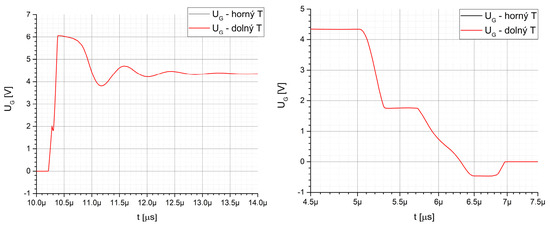
Figure 19.
Simulation results for GaN module driving_v3—details of the gate–source voltage during turn-on (left) and turn-off (right) process.
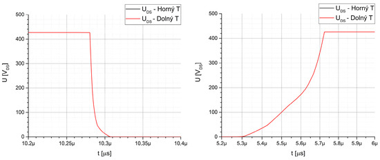
Figure 20.
Simulation results for GaN module driving_v3—details of the drain–source voltage during turn-on (left) and turn-off (right) process.
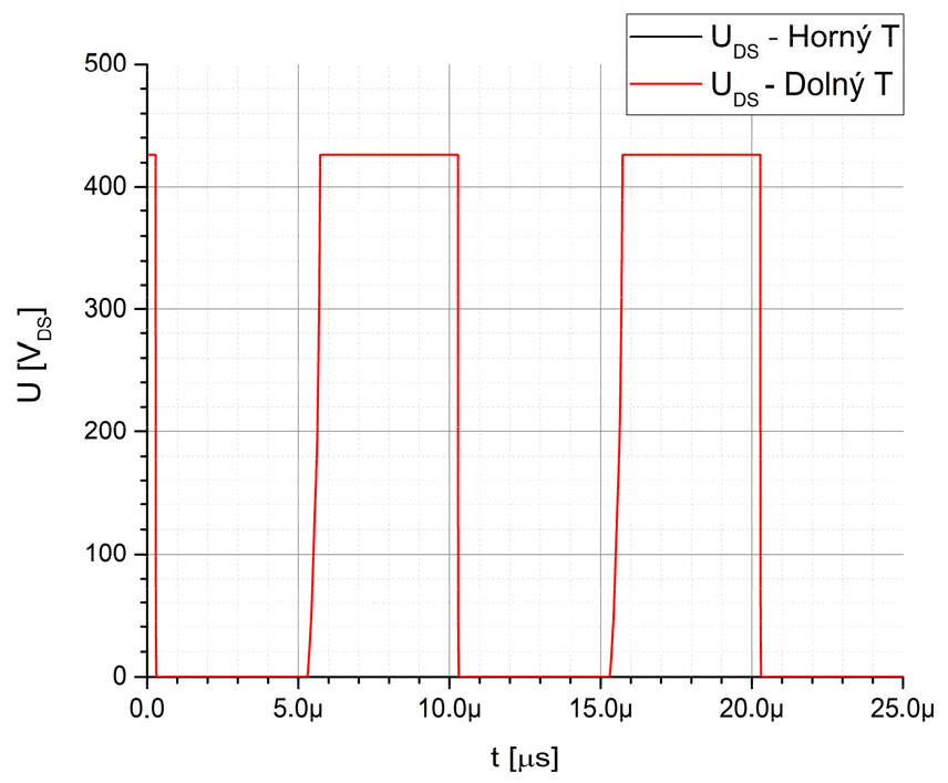
The drain–source voltages during the switching sequence are seen in Figure 21. It is seen that the voltage redistribution within the transistors of the stacked GaN module is in an ideal state. So, under the given conditions and based on the simulation, this configuration is the most suitable for application use. Due to this fact, the experimental testing of the GaN transistor stacked module was performed for the selected types of power transistors considering driving configuration with the pulsed transformer.
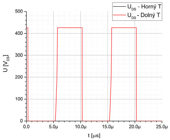
Figure 21.
Simulation results for GaN module driving_v3—waveforms of drain–source voltage during switching sequence.
4. Experimental Analysis of Selected Driving Technique
As was previously mentioned, driving configuration v_3 performed the best according to the voltage redistribution and turn-on/turn-off timing of driving signals. The experimental testing was realized in laboratory conditions, while the circuit parameters and circuit configuration (Figure 7) during testing are the same as the first simulation:
- Input voltage: 100 V–400 V;
- Output voltage: 200 V–800 V;
- Output power: max 600 W (the load was constantly set to RLoad = 1.14 kΩ);
- Switching frequency: 100 kHz;
- Duty cycle: D = 0.5;
- Driving voltage range 0 V ÷ 5 V.
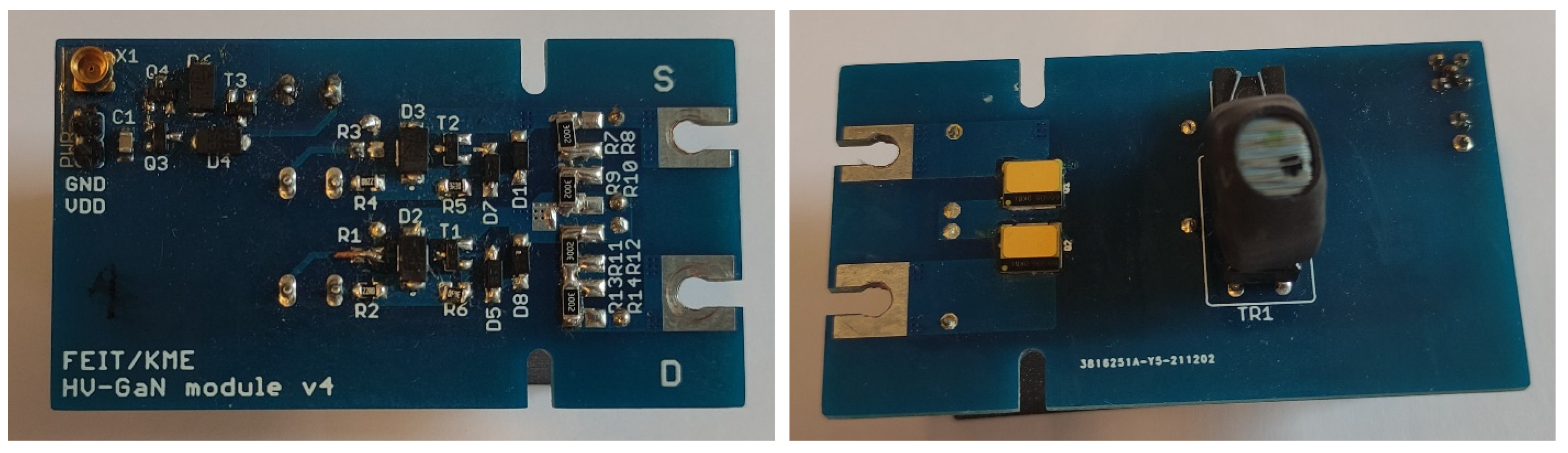
The aim of the experimental verification is to test whether the driving configuration of the GaN-stacked transistor is able to meet high voltage operation (above 650 V), as such GaN transistors are not available on the market as a single transistor device. Figure 22 shows circuit schematics of the experimental sample. The primary side represents the driving circuit of the pulsed transformer, which is formed by a totem-pole configuration (NPN and PNP transistors) and the demagnetization circuit of the transformer (D4, D6, and T3). On the secondary side, there is a driving circuit composed of an N-channel MOSFET and diodes (D2, D3, T1, and T2). The task of this circuit is to ensure that the transistors are excited at the same time while remaining isolated from each other. To reduce the parasites, professional printed circuit boards (Figure 23) were realized for both types of the tested transistors (GaN Systems and Nexperia).
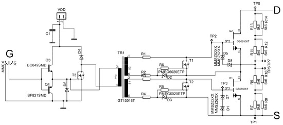
Figure 22.
Circuit schematic of GaN module for v3 configuration of driving circuit.

Figure 23.
Experimental sample of stacked GaN module using GaN Systems transistors and pulsed transformer driving configuration.
4.1. GaN Systems Stacked Module
Figure 23 represents the experimental sample for the case of the GaN Systems transistor testing. On the left side (top view) you can see the elements of the driver circuit and its passive components. On the right (bottom view) you can see the transistors connected in series (stacked configuration) and the pulse transformer. As was mentioned at the beginning of this section, the measurements were performed under the same conditions as the simulation experiments. The results are therefore compared to the results obtained from the simulation analysis. The initial values are listed in Table 1 and Table 2, while later the main variables, which indicate the performance of the module, are reported using graphs (Figure 24).

Table 1.
Values of variables for performance evaluation of GaN Systems module_v3_simulation results.
Table 2.
Values of variables for performance evaluation of GaN Systems module_v3_experimental measurements.
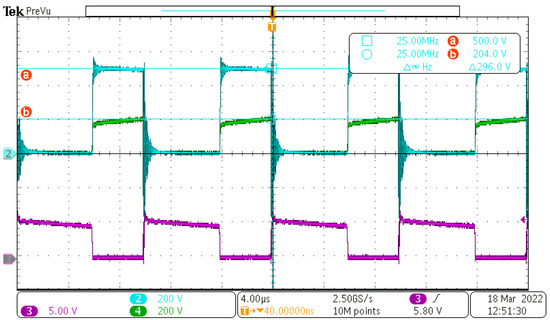
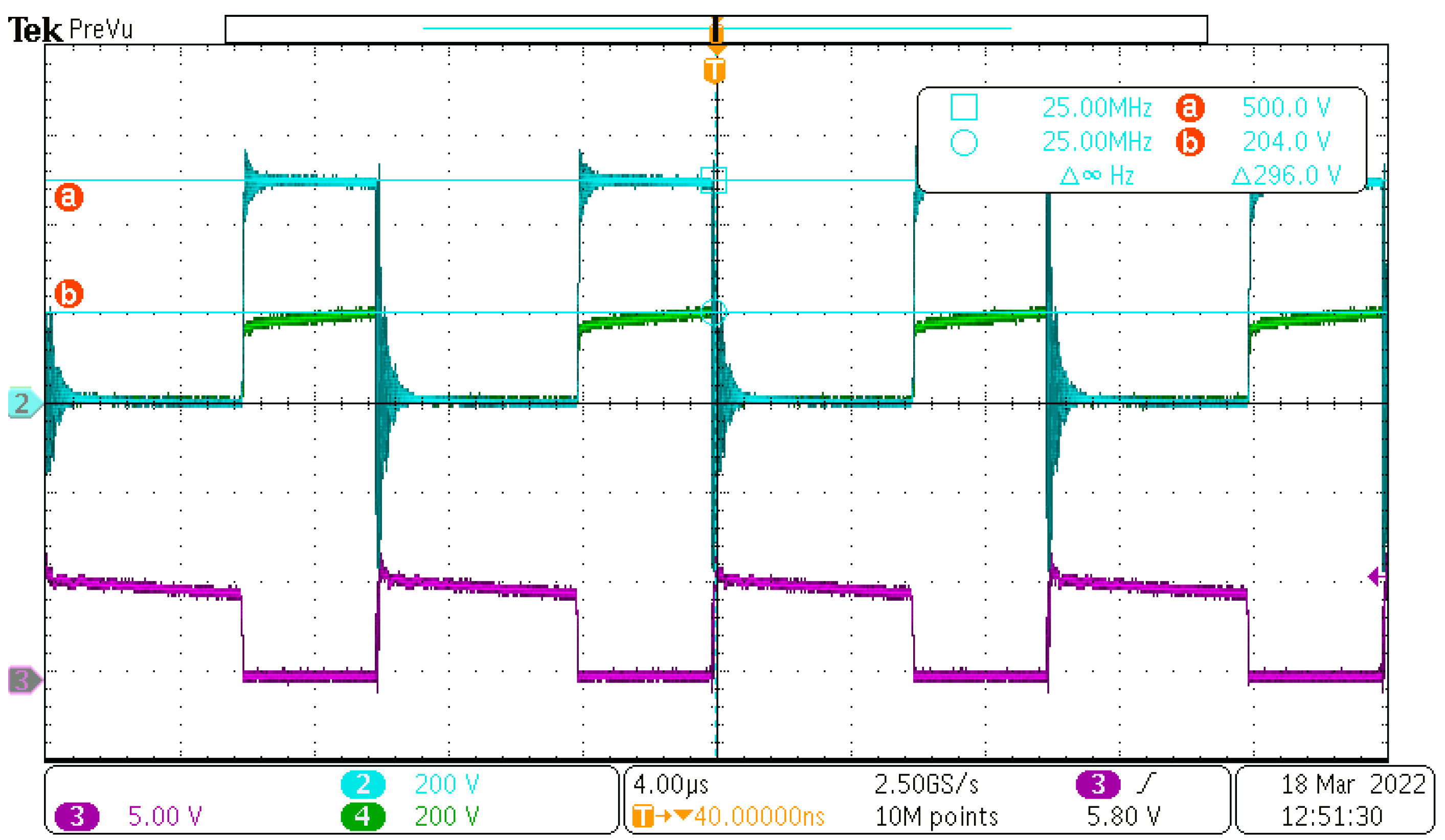
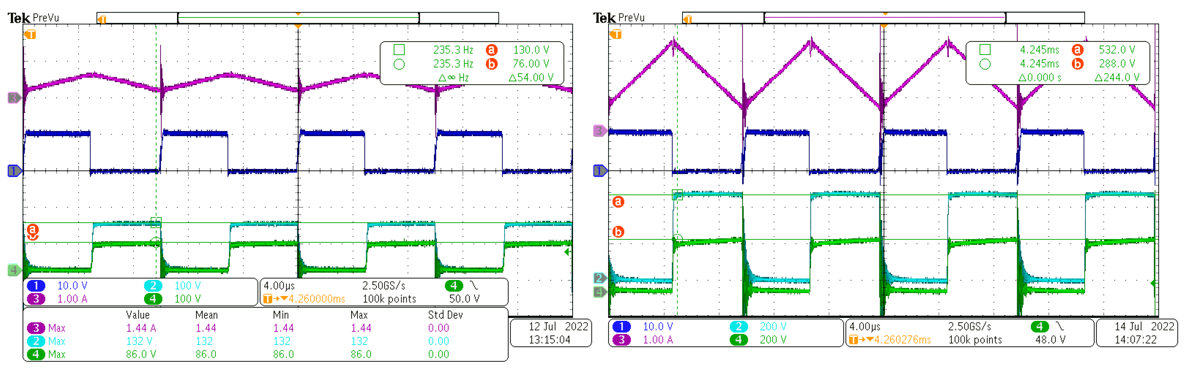
Figure 24.
Time waveforms of top transistor drain–source voltage (light blue), bottom transistor drain–source voltage (green) and gate–source voltage of GaN module situation for 350 V of input voltage.
From the tables it is seen that the coefficient “k” is evaluated as well. This parameter refers to the percentage deviation of the voltage between the top and bottom transistor in the GaN-stacked module. Once the ideal situation occurs (the results from the simulation), then UDS_TOP = UDS_BOTTOM. The calculation of this coefficient is as follows:
where UDS_TOP is the drain–source voltage of the top transistor and UDS_BOTTOM is the drain–source voltage of the bottom transistor. From the results in Table 1 and Table 2, it is seen that in the experimental part, the deviation is at the level of 30%. This was not presented in the simulation experiments.
The main reason why this deviation applies to the experimental part is that there are more crucial side effects of the parasitic components within the driving and power circuit. The bottom waveform represents the gate–source voltage of the GaN-stacked module. This result is valid for the last measurement in Table 2, i.e., for 350 V of input voltage, the output voltage was 704 V, i.e., the blocking voltage of the GaN module.
In Figure 25, you can see a comparison of the measured and simulated efficiency of the high-voltage GaN module_v3. In this case, the experimental measurements took place at a reduced output power, but as you can see from the graph, the efficiency values are very similar in both cases and reach an average value of 97%. The nominal power operation was not realized because the voltage deviation was high, causing the destruction of the power transistor.
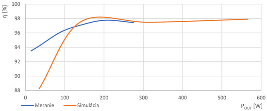
Figure 25.
Evaluation and comparison of the efficiency of the GaN system stacked module, equipped within a boost converter circuit (measured for 350 V of input voltage).
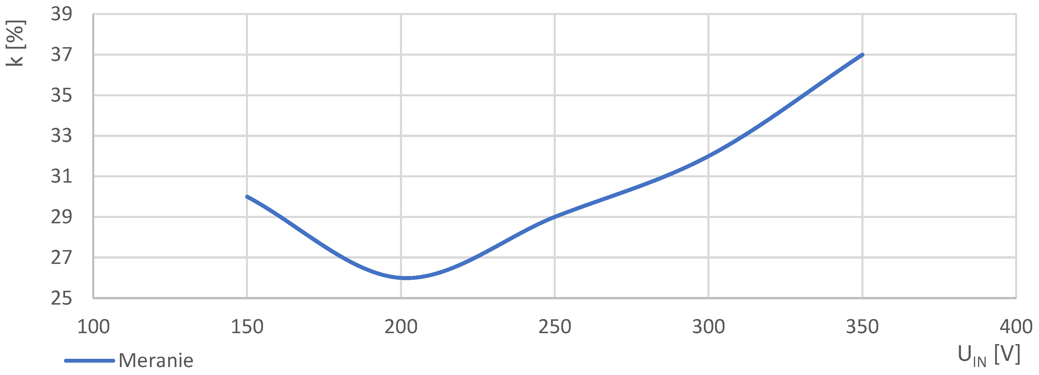
The percentage of the voltage deviation between the transistors of the stacked GaN module with GaN Systems transistors is plotted in Figure 26, while the dependency variable is the input voltage. From the simulations, it was expected that the ideal state will be achieved (zero deviation). However, mainly due to parasites and their nonlinear behavior, the experiments showed deviation ranging from 25% to 37%.
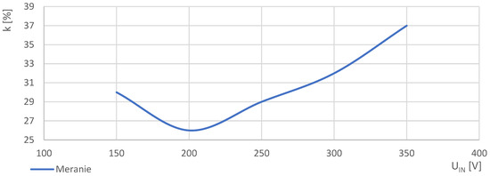
Figure 26.
Percentage UDS voltage deviation of the transistors in the GaN Systems stacked module.
The nonlinearities of the parasitic capacitances of the transistors play a crucial role during the commutation intervals. Their behavior cannot be modeled perfectly using simulation tools, so it is hard to observe during computer analyses. Their effect was applied within the laboratory prototypes of stacked modules. It is not possible to eliminate this behavior during the operation.
Based on the facts mentioned above, this high-voltage GaN module equipped with GaN Systems transistors is not suitable for the operation of the converter at high voltages, since the maximum voltage reached was 700 V and subsequently, one of the transistors broke down.
4.2. Nexperia Transistor Stacked Module
In the previous module configuration, it was not possible to reach the required blocking voltage value, so the same configuration with another type of GaN transistor from a different manufacturer was realized. In this case, Nexperia’s GAN039-650NBB transistors were used. The principle of operation is the same as in the previous case, with the v3 driving circuit being utilized. This stacked GaN module is shown in Figure 27. Following the design, we moved on to testing the sample again.
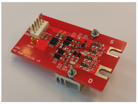
Figure 27.
Experimental sample of stacked GaN module using NeXperia transistors and pulsed transformer driving configuration.
Table 3 presents the measured results. From the table, it is seen that the blocking voltage of the module reached 775V at the maximum value of the input voltage (400 V) without damaging the module. At the given voltage, an efficiency of 95% was achieved, while the nominal power operation was achieved as well. The simulation results are not presented here in either table or graph form because NeXperia does not provide the relevant simulation model of the device.
Table 3.
Values of variables for performance evaluation of NeXperia module_v3_experimental measurements.
The next figure (Figure 28) shows the time waveforms from experiments. Here, the inductor current is shown, together with the voltages on the module–driving voltage UG (blue course) and the drain–source voltage UDS on the transistors (light blue course—upper transistor, green course—lower transistor).
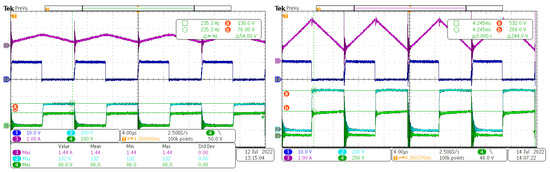
Figure 28.
Time waveforms of inductor current (violet) top transistor drain–source voltage (light blue), bottom transistor drain–source voltage (green), and gate–source voltage of GaN module.
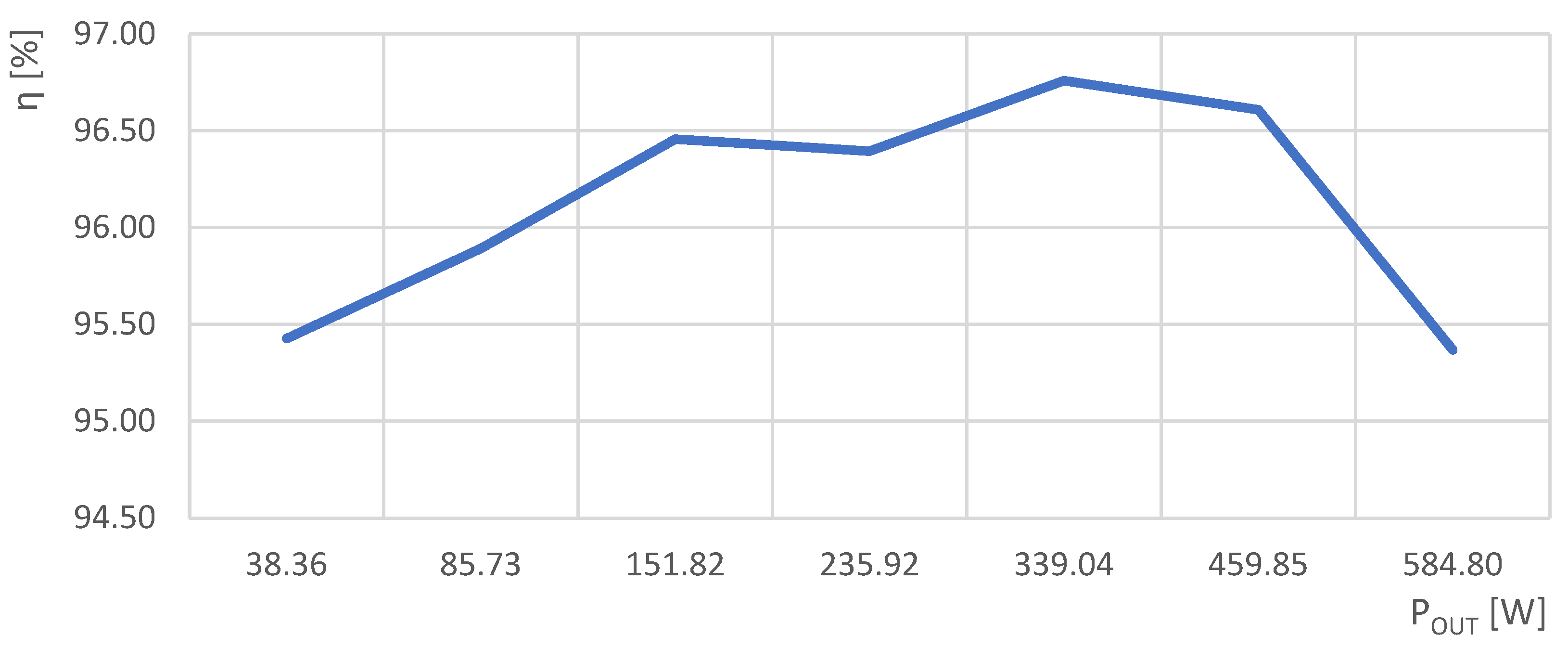
The graphical interpretation of the efficiency of dependency on power is shown in Figure 29. This efficiency was evaluated for the maximal value of the input voltage (400 V). The maximum value was 96.6%, while for the nominal power application, 95.5% was achieved. In comparison to the GaN Systems stacked module, the efficiency is lower (due to the technology of the device); however, in this case nominal power and nominal voltage operation were achieved reliably.
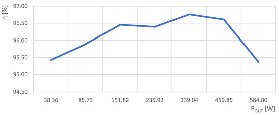
Figure 29.
Evaluation and comparison of the efficiency of NeXperia GaN module equipped within a boost converter circuit (input voltage = 400 V).
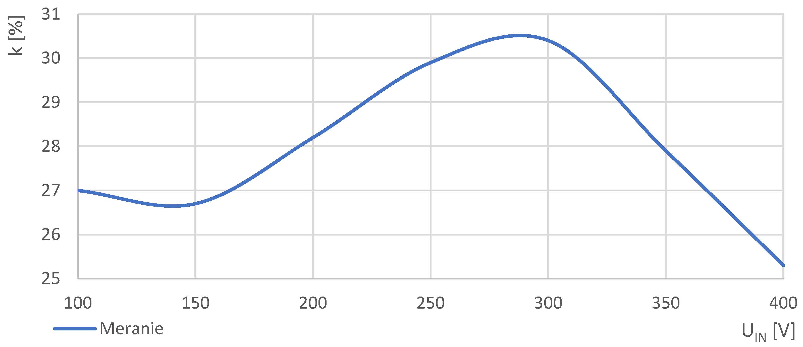
In Figure 30, a graphical interpretation of the k-parameter is reported. For this situation, the deviation was lower than in the previous cases, and it did not affect the operation of the converter.
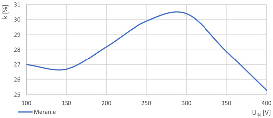
Figure 30.
Percentage UDS voltage deviation of the transistors in the NeXperia stacked module.
In terms of the main requirement for stacked configuration evaluation, a blocking voltage of the DC link of 800 V was achieved, which unlike the previous version with transistors from GaN Systems, was not possible. The main reason should be a more robust structure of NeXPeria components (cascode connection and internal excitation using an N-channel MOSFET). This enables a higher threshold voltage and higher values of driving signals; thus, they are more resistant to interference.
5. Conclusions
The development of high-power electronics has been a significant focus in recent years, driven by the increasing demand for efficient and reliable power conversion systems. The design of high-voltage stacked GaN modules requires careful consideration of various factors, including device integration and reliability. Device integration is a critical aspect, as the high-voltage stacked configuration requires the careful integration of multiple GaN devices to achieve the desired voltage and current ratings.
In this paper, the main focus was given to the design considerations of the stacked GaN module, while the driving circuit of this module was the main aspect under investigation. Initially, two technologically indifferent GaN power transistors were introduced as options for the module design. Later, three different alternatives for the driving circuits were presented. Firstly, those variants were evaluated through simulation experiments, while one of the GaN transistor alternatives was used. The focus was given to the timing and dynamics of the driving signals, and on the drain–source voltage deviation of individual transistors forming the stacked configuration. Based on the simulation analyses, the driving technique utilizing a pulsed transformer was selected as the best alternative for practical use. Therefore, experimental samples of stacked modules equipped with selected GaN transistors and the driving circuit were designed.
Laboratory experiments were conducted under a boost converter circuit configuration, with the operational parameters being the same as in the simulations. Firstly, the GaN Systems stacked module was examined. It was found that the results were different than those achieved by the simulation. The main difference was evident within the drain–source voltage deviation of the individual transistors forming the stacked module. The value of this parameter approached more than 35% for a certain value of the input voltage. The expectations to meet the value of blocking voltage at the level of 800 V were not satisfied, and the stacked module was damaged due to the fact that the voltage-blocking capability of the one of transistors from the stacked module was exceeded. On the other hand, the results of the simulation and experimental measurement have been identified as the same. Secondly, the experimental sample of a stacked module equipped by NeXperia transistors and the selected alternative of the driving circuit exhibited satisfactory results. The requirement of the 800 V voltage-blocking capability was met for the nominal input voltage. Simultaneously, the nominal power was also capable of being delivered, while the stable operation within the whole power range was observed. The voltage deviation was reduced to 25% compared to the first sample.
Based on these results, it was found that the configuration of the driving circuit has a very significant influence on the operational behavior of stacked module configurations. Also, the technology of the power semiconductor device affects the operational characteristics of the configuration. Future work will be addressed to verify operations for higher switching frequencies and later, make comparisons to SiC power transistor performances.
Author Contributions
Conceptualization, methodology, formal analysis, and writing, M.F.; validation and data curation, R.Z.; supervision and review, P.S. All authors have read and agreed to the published version of the manuscript.
Funding
This research was funded by the National Grant Agency VEGA for the project Nr 1/0274/24.
Data Availability Statement
No new data were created or analyzed in this study. Data sharing is not applicable to this article. The original contributions presented in the study are included in the article.
Acknowledgments
The authors would like to thank the National Grant Agency APVV for the project funding APVV-21-0462 and to the National Grant Agency Vega for project funding 1/0274/24.
Conflicts of Interest
The authors declare no conflicts of interest.
References
- Juncheng, L.; Di Maso, P. GaN Enables Efficient, Cost-Effective 800V EV Traction, EDN—Electronics Community for Engineers. 22 May 2020. Available online: https://www.edn.com/gan-enables-efficient-cost-effective-800v-ev-traction-inverters/ (accessed on 15 March 2023).
- McDonald, T.; Butler, S.W. Progress and Current Topics of JEDEC JC-70.1 Power GaN Device Quality and Reliability Standards Activity: Or: What is the Avalanche capability of your GaN Transistor? In Proceedings of the 2021 IEEE International Reliability Physics Symposium (IRPS), Monterey, CA, USA, 21–25 March 2021; pp. 1–6. [Google Scholar] [CrossRef]
- Koscelnik, J.; Prazenica, M.; Frivaldsky, M.; Ondirko, S. Design and Simulation of Multi-element Resonant LCTLC Converter with HF Transformer. In Proceedings of the ELEKTRO 10th International Conference, Rajecke Teplice, Slovakia, 19–20 May 2014. [Google Scholar]
- Custer, J.; Formicone, G.; Walker, J.L.B. Recent advances in kW-level pulsed GaN transistors with very high efficiency. In Proceedings of the 2016 21st International Conference on Microwave, Radar and Wireless Communications (MIKON), Krakow, Poland, 9–11 May 2016; pp. 1–4. [Google Scholar] [CrossRef]
- GCantone; Pulvirenti, F. Integrated solutions and related technologies for gate drivers of GaN transistors. In Proceedings of the 2020 AEIT International Annual Conference (AEIT), Catania, Italy, 23–25 September 2020; pp. 1–6. [Google Scholar] [CrossRef]
- Dobrucky, B.; Kascak, S.; Prazenica, M.; Jarabicova, M. Improving Efficiency of Hybrid Electric Vehicle Using Matrix Converters. Elektron. Elektrotechnika 2019, 25, 29–35. [Google Scholar] [CrossRef]
- Briz, P.; Sarnago, H.; Burdío, J.M.; Lucía, O. High-Voltage Nanosecond Pulse Generator Using Series-Stacked Enhancement-Mode GaN Transistors. In Proceedings of the 2024 IEEE Applied Power Electronics Conference and Exposition (APEC), Long Beach, CA, USA, 25–29 February 2024; pp. 3179–3183. [Google Scholar] [CrossRef]
- Kascak, S.; Prazenica, M.; Jarabicova, M.; Paskala, M. Interleaved DC/DC Boost Converter with Coupled Inductors. Adv. Electr. Electron. Eng. 2018, 16, 147–154. [Google Scholar] [CrossRef]
- Ho, C.-Y.; Liang, T.-J.; Chen, K.-H.; Liao, K.-F. Design and Implementation of Cascoded Dual-Half-Bridge Resonant Converter with GaN E-HEMT for High Input Voltage Applications. In Proceedings of the 2024 IEEE Applied Power Electronics Conference and Exposition (APEC), Long Beach, CA, USA, 16–20 March 2024; pp. 114–121. [Google Scholar] [CrossRef]
- Shojaie, M.; Elsayad, N.; Mohammed, O.A. Design of an all-GaN bidirectional DC-DC converter for medium voltage DC ship power systems using series-stacked GaN modules. In Proceedings of the 2018 IEEE Applied Power Electronics Conference and Exposition (APEC), San Antonio, TX, USA, 4–8 March 2018; pp. 2155–2161. [Google Scholar]
- GN008: GaN Switching Loss Simulation Using LTSpice 05/2018. Available online: https://gansystems.com/ (accessed on 16 June 2023).
- Spanik, P.; Dobrucky, B.; Frivaldsky, M.; Drgoňa, P.; Kurytnik, I. Measurement of swtitching losses in power transistor structure. Elektron. Elektrotechnika 2008, 82, 75–78. [Google Scholar]
- Frivaldský, I.M.; Drgoňa, P.; Spanik, P. Experimental analysis and optimization of key parameters of ZVS mode and its application in the proposed LLC converter designed for distributed power system application. Int. J. Electr. Power Energy Syst. 2013, 47, 448–456. [Google Scholar] [CrossRef]
- Frivaldský, M.; Dobrucky, B.; Prazenica, M.; Koscelnik, J. Multi-tank resonant topologies as key design factors for reliability improvement of power converter for power energy applications. Electr. Eng. 2015, 97, 287–302. [Google Scholar] [CrossRef]
- Kandrac, J.; Frivaldsky, M.; Prazenica, M.; Simonova, A. Design and Verification of proposed Operation Modes of LLC Converter. Elektron. Elektrotechnika 2012, 18, 27–30. [Google Scholar] [CrossRef]
- Augutis, V.; Gailius, D.; Styra, D.; Dumčius, A. Transistor Control with Additional Charge Pumping Circuit. Elektron. Elektrotechnika 2007, 78, 79–82. [Google Scholar]
- Kascak, S.; Laskody, T.; Prazenica, M.; Konarik, R. Current control contribution to a single-phase induction motor fed by single-leg voltage source inverter. In Proceedings of the 2016 ELEKTRO, Strbske Pleso, Slovakia, 16–18 May 2016; pp. 172–175. [Google Scholar] [CrossRef]
- Hruska, K.; Kindl, V.; Pechanek, R. Design of a high-speed permanent magnet synchronous motor for electric kart. Electr. Eng. 2017, 99, 1141–1150. [Google Scholar] [CrossRef]
- Varecha, P.; Makys, P.; Pacha, M.; Zossak, S. Effect of MOSFET lifetime on reliability of low-side MOSFET current sensing technique. In Proceedings of the 2020 ELEKTRO, Taormina, Italy, 25–28 May 2020; pp. 1–6. [Google Scholar] [CrossRef]
- Hsia, C.; Li, C.-Y.; Lu, D.-F.; Chen, T.-Y. Integrated All-GaN Driver for High-voltage DC-DC Power Converters. In Proceedings of the 2023 20th International SoC Design Conference (ISOCC), Jeju, Republic of Korea, 28–28 October 2023; pp. 175–176. [Google Scholar] [CrossRef]
- Otsu, S.; Ujita, S.; Tanaka, K.; Maede, M.; Niimi, H.; Ochi, S. A 2 × 2 paralleling GaN half-bridge power module for high-density 500kHz 3.3kW CLLC converter. In Proceedings of the 2023 IEEE Applied Power Electronics Conference and Exposition (APEC), Orlando, FL, USA, 19–23 March 2023; pp. 1627–1632. [Google Scholar] [CrossRef]
- Zelnik, R.; Pipiska, M. Simulation analysis of switching performance of GaN power transistors in a high-voltage configuration. In Proceedings of the 2020 21st International Scientific Conference on Electric Power Engineering (EPE), Prague, Czech Republic, 19–21 October 2020; pp. 1–6. [Google Scholar] [CrossRef]
- Shojaie, M.; Elsayad, N.; Moradisizkoohi, H.; Mohammed, O.A. Design and Experimental Verification of a High-Voltage Series-Stacked GaN eHEMT Module for Electric Vehicle Applications. IEEE Trans. Transp. Electrif. 2019, 5, 31–47. [Google Scholar] [CrossRef]


Disclaimer/Publisher’s Note: The statements, opinions and data contained in all publications are solely those of the individual author(s) and contributor(s) and not of MDPI and/or the editor(s). MDPI and/or the editor(s) disclaim responsibility for any injury to people or property resulting from any ideas, methods, instructions or products referred to in the content. |
© 2024 by the authors. Licensee MDPI, Basel, Switzerland. This article is an open access article distributed under the terms and conditions of the Creative Commons Attribution (CC BY) license (https://creativecommons.org/licenses/by/4.0/).