Article

Design and Simulation of Low-Orbit Satellite Broadcast Signal Receiving and Processing Terminal

Radar Technology Research Institute, School of Information and Electronics, Beijing Institute of Technology, Ministry of Education, Beijing 100081, China
*
Author to whom correspondence should be addressed.
Electronics 2024, 13(16), 3270; https://doi.org/10.3390/electronics13163270
Submission received: 20 June 2024 / Revised: 8 August 2024 / Accepted: 14 August 2024 / Published: 17 August 2024
(This article belongs to the Section Circuit and Signal Processing)

Abstract

:
As an important space-based intelligence acquisition and combat command receiving component, the low-orbit satellite broadcast signal receiving terminal is an important guarantee for realizing the full-dimensional joint operations of our military’s multi-services. This design is based on the SoC platform. Compared to the traditional low-orbit reconnaissance satellite reception and processing terminal business process, a narrowband anti-interference module is added and the interference-to-signal ratio reaches 57 dB and 47 dB when resisting interference from a single frequency band and three frequency bands, respectively. Digital beamforming is used for signal processing and beamforming gain of the whole machine reaches 14–15 dBic; compared to traditional capture and tracking modules, this terminal uses a time domain parallel frequency domain FFT fast acquisition method and a bit synchronization loop is added to the tracking loop to aiming at the problem that the frequency signal acquisition speed is not fast enough and addressing the issue that information symbol rate is not an integer multiple of the pseudo-code, thus complete bit synchronization within 60 ms, with a bit error rate of 0; the coding gain can reach 7 dB. Combined with the solution of decoding and positioning solution algorithms, this scheme used the JFM7K325T chip to complete the design simulation of the complete receiving and processing terminal.

1. Introduction

In recent years, with the rapid development of science and technology, satellite communication has gradually become one of the most promising research directions in the current communication industry. Satellite communication is a form of communication that is not restricted by natural conditions such as terrain, landform, and climate, nor is it interfered with by human factors such as national boundaries, politics, and economy, and can achieve information transmission between any two points. Satellite broadcasting signal reception is an important part of the satellite communication process, so research on the reception and processing of satellite broadcasting signals has important theoretical and practical significance [1,2,3].
In today’s satellite communication field, low-orbit satellites have gradually attracted attention and favor in the world’s satellite navigation field with their unique advantages in constellations and signals. The US Iridium system and the GPS jointly developed and launched a new satellite timing and positioning service (STL) based on low-orbit satellites, which has become a backup or supplement to the GPS system; the European Galileo system technical team is also actively promoting the research on the Kepler system, through a low-orbit constellation composed of 4–6 low-orbit satellites, and through inter-satellite links to monitor and measure medium and high-orbit satellites with high precision, so as to greatly improve the orbit determination accuracy of the Galileo constellation. China’s low-orbit satellite technology is also developing in full swing. Low-orbit satellite constellations such as Hongyan, Integrated Space-Earth Network, and MicrocentiSpace have carried out in-orbit tests of experimental satellites [1,3,4,5,6].
For military uses, the low-orbit satellite broadcast signal receiving terminal is an important space-based intelligence acquisition and combat command receiving component for the realization of the military’s multi-service full-dimensional joint operations. In actual military applications, low-orbit reconnaissance satellites will detect enemy targets, process the reconnaissance results on the satellite, and report the results to other satellites or distribute them to the receiving terminals of our detection unit. Finally, the reconnaissance unit will process the results [1,3,7,8].
Low-orbit satellites can provide low-latency, high-speed, and high-reliability mobile communication services. In low-orbit satellite communication scenarios, the movement of the satellite carrier will cause the receiver to have a large Doppler frequency shift and rate of change during the transmission process, requiring high-performance signal capture, tracking, and anti-interference technology to achieve signal synchronization [2,4,5,6]. This article mainly studies how to achieve the reception and processing of low-orbit satellite broadcast signals in the current complex electromagnetic interference environment.
Digital beamforming uses digital phase shifting to compensate for the phase difference caused by the path difference caused by the inconsistent RF channel delay and the spatial distance difference for the incident signal in a certain direction, so as to achieve in-phase superposition, thereby achieving the maximum energy reception in that direction and completing the beamforming in that direction to receive the useful desired signal. By changing the beam weight value, the beam is pointed in different directions to achieve beam scanning. Through multi-channel parallel processing, beams in multiple directions are formed at the same time [9]. You can also select a suitable window function to reduce the intensity of the sidelobe level. Beamforming ensures the consistency of the multi-channel phase by correcting the signal phase, and then directly accumulates the multi-channel data to increase the signal power. The antenna using digital beamforming has good self-correction and low sidelobe performance. These advantages of digital beamforming are not available in modular beamforming and have a far-reaching impact on improving the performance of the receiver [10]. Although digital beamforming has been widely valued in the field of military radar due to its unique functions and advantages, its application is restricted by the accuracy and gain of beamforming. Therefore, as digital beamforming technology develops, how to improve its accuracy and gain has also received widespread attention at home and abroad [9,10,11,12].
Narrowband interference refers to interference with a signal bandwidth much smaller than the RF signal bandwidth, including single-tone interference, multi-tone interference, narrowband random processes, and low-rate digital signals. Narrowband interference is usually defined as an interference signal with an interference frequency band no greater than one-tenth of the signal frequency band. Therefore, for any satellite signal, narrowband interference signals are widespread. Each navigation satellite transmits carrier radio signals at two L frequencies (i.e., L1 and L2) [6]. In communication confrontation scenarios, since narrowband interference (NBI) is easy to generate, the power spectrum density can be very high, and a few narrowband interferences can cover a certain width. Compared with broadband suppression interference, it is more conducive to interfering with the opponent’s system and ensuring the normal operation of one’s own system. Therefore, narrowband interference is very common, and the effective means of implementing anti-narrowband interference is one of the issues worthy of key research in the current field of satellite signal reception and processing [2].
The purpose of spread spectrum signal capture is to obtain a rough estimate of the carrier frequency and code phase of all visible satellites, which is the premise for the receiver tracking loop to successfully track GPS satellite signals. At present, many scholars at home and abroad have designed and used different capture methods for various scenarios, but any method has its own trade-offs between computational complexity, hardware cost, and limitations in the scope of application. Even the most commonly used PMF-FFT method in the current communication confrontation field can effectively combine matched filtering with frequency domain parallel capture methods, compensate for their respective disadvantages while taking into consideration the advantages of both, and greatly reduce the number of FFT operation points and complexity when using filters. It can stably capture signals in weak signal and high dynamic scenarios, but it still needs to align the symbol rate with the spread spectrum code [5]. In order to solve this problem, it is necessary to generate a spread spectrum code period interrupt and perform incoherent operations, which will cause a significant increase in the amount of calculation, making it difficult to meet the high real-time and high sensitivity requirements in the current communication confrontation scenario. How to solve the problem of aligning the symbol rate and spread spectrum code during capture under the requirements of high real-time and high sensitivity capture is of great research significance [8].
The issues studied in this paper are: (1) Aiming at the problem of determining the amplitude and phase weighting coefficients of the signals of each array element required in different directions, a digital beamforming technology is proposed while taking into account the low sidelobes and constant gain of the array beam; (2) Addressing the issue that time domain anti-interference method requires a large amount of prior information and that two transformations of frequency domain anti-interference method require a large amount of computing resources, an interference suppression technology that combines time and frequency domains is proposed [2,5]. Combining the advantages that frequency domain notching does not require prior information and frequency point estimation is more accurate, and the time domain notching can completely eliminate interference, then avoiding their respective shortcomings; (3) Aiming at the problem that the frequency signal acquisition speed is not fast enough and the problem led by information symbol rate is not an integer multiple of the pseudo-code rate while using the PMF-FFT algorithm [3,4], the three-loop tracking technology with the bit synchronization loop is introduced into the tracking loop to increase the acquisition speed, achieve a large doppler frequency shift, enough acquisition sensitivity and precise loop control [7,8]; (4) Combining data demodulation, RS decoding technology and positioning solution algorithm and based on the FPGA digital processing board, the JFM7K325T chip is used to design the FPGA, thereby realizing the complete design simulation of the low-orbit satellite broadcast signal processing terminal.

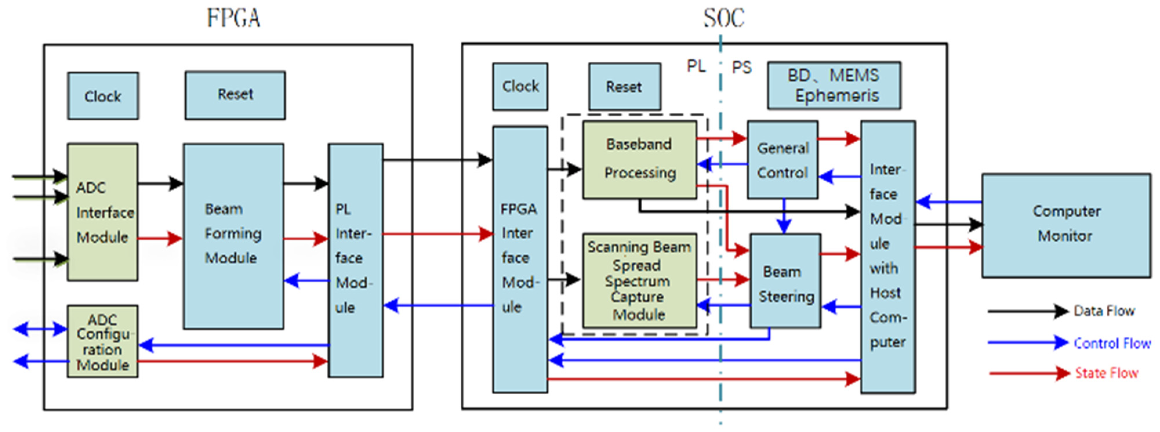
2. Overall System Design

The complete data processing flow chart of low-orbit satellite signals on the satellite and on the ground is shown in Figure 1. The core steps of the processing flow on the satellite include two frequency conversions, that is, the encoded I and Q channel data process directly spread spectrum (spread spectrum code rate 10.23 MHz, code length 1023) and spectrum shifting (QPSK modulation) to the radio frequency band of 2~3 GHz for transmission. The processing flow of the receiving terminal on the ground is the reverse process of the processing flow on the satellite [1,3].
Among them, the processing flow of the receiving terminal on the ground is shown in Figure 2. The receiving terminal achieves signal reception and processing in complex electromagnetic interference environments through signal processing such as radio frequency processing, ADC, narrowband anti-interference, digital beamforming, filter, extraction and truncation, and information processing such as capture, tracking, bit synchronization, frame synchronization, data demodulation, message decoding, and positioning operations.
According to the independence of functions of each part in the above-mentioned low-orbit satellite signal processing flow on the satellite and on the ground, the system can be divided into four blocks: antenna array, radio frequency unit, baseband processing board and application processing terminal [1,6], as shown in Figure 3. Among them, the antenna array filters and amplifies the signal and then transmits it to the radio frequency local oscillator board; the radio frequency unit is responsible for moving the radio frequency signal received by the antenna array to an intermediate frequency nearby, which facilitates the subsequent baseband board to perform beamforming, acquisition and tracking process; the baseband processing board is mainly responsible for the IF signal sent from the radio frequency module to process AD conversion, beamforming, acquisition, tracking, demodulation and decoding, etc., then the processed baseband signal is sent to the application processing terminal; the data processing terminal is mainly responsible for interacting with the receiver and presents the results to users.

3. Key Technologies

3.1. Digital Beamforming Technology

In the business process of traditional low-orbit reconnaissance satellite reception and processing terminals, satellite broadcast signals cannot meet the coverage requirements of high-gain multi-beams [10]. Based on this problem, this design proposes digital beamforming technology, taking low sidelobes and constant gain of array beams into account.
Digital beamforming uses digital phase shifting to compensate for the phase difference caused by the path difference caused by the inconsistent RF channel delay and the spatial distance difference for the incident signal in a certain direction, so as to achieve in-phase superposition, thereby achieving the maximum energy reception in that direction and completing the beamforming in that direction to receive the useful desired signal [9,11,12,13,14,15,16,17]. By changing the beam weight value, the beam is pointed in different directions to achieve beam scanning. Through multi-channel parallel processing, beams in multiple directions are formed at the same time. You can also select a suitable window function to reduce the intensity of the sidelobe level. Beamforming ensures the consistency of the multi-channel phase by correcting the signal phase, and then directly accumulates the multi-channel data to increase the signal power. Compared with analog beamforming, the antenna using DBF has better self-correction and low sidelobe performance, which has a far-reaching impact on improving the performance of the receiver [14].
Digital beamforming processes the array received signal in the digital domain and uses the digital beamforming algorithm to calculate the optimal adaptive weighting vector so that the main lobe of the antenna pattern points to the desired direction and the null is aligned with the interference direction, thereby achieving the purpose of spatial domain filtering [14,15]. Array signal processing in the digital domain can use advanced digital processing technology to make the processing process more flexible and controllable. When the array parameters and target parameters are accurately known, DBF can be used to obtain an approximate optimal output signal-to-interference-to-noise ratio, so that the array antenna can achieve better signal resolution and parameter estimation performance [12,18]. However, in practical applications, the existence of various errors and non-ideal factors will cause deviations in the steering vector of the desired signal, resulting in a decrease in the gain of the desired signal or even cancellation of the desired signal, which deteriorates the output performance. In addition, high computational complexity is also a problem faced by digital beamforming technology in engineering applications [17]. Therefore, efficient and robust beamforming algorithms have important research significance and practical value.
Before signal superposition, digital beamforming needs to adjust the phase between the data of each channel to ensure that the phase error is within a certain range so that the data of each channel can be superimposed to improve the received power and signal-to-noise ratio of the received signal. The digital beamforming software structure is divided into two aspects: beam control and beamforming. Among them, the role of beam control is to align the main beam of the antenna array with the direction of the useful signal, so that the subsequent beam synthesis can maximize the gain of the synthesized useful signal; the role of beam synthesis is to synthesize the useful signal. The control method in this scheme adopts a method based on prior information and spatial domain search. The beam direction is determined by logical control, and then the phase difference between the required superimposed signals is extracted. After compensating for the phase, the beam is superimposed to complete the beamforming [11,14,18]. The schematic diagram is shown in Figure 4.
Among them, the first stage of beam steering first works based on a priori information. The beam directions of different satellites are calculated based on the a priori information, the beam-forming parameters of the corresponding satellites are read through the look-up table, and the beam-forming parameters are assigned to different channels, ultimately verifying the effectiveness of beamforming. If it is invalid, determine whether the satellite has transited. If it has transited, stop the beam-forming process [12,15,17]; if it has not transited, jump to beamforming based on airspace search. Initially, complete the beam acquisition of different satellites according to the preset beam pointing parameters; then each satellite is searched within a certain angle range from the direction of the captured beam, and then spread spectrum tracking verification and power comparison are performed. The beam direction with the highest power is selected as the tracking result and assigned to the beam-forming channel of the corresponding satellite [17,18,19].
Considering that each communication time of low-orbit satellites is short and the beam changes quickly, the beamforming in the second stage mainly uses the look-up table method [12,18]. The weighting coefficients in different directions are calculated through simulation analysis and the coefficients are solidified in the memory. Then, extract the weighting coefficient according to the specific pointing parameter for beam synthesis. The advantages of this method are less calculation, fast running speed, and simple algorithm design [15,19].
In the scheme, each unit of the beam is optimized with amplitude weighting, such as Taylor distribution or Chebyshev distribution, to achieve low sidelobe characteristics of the array beam [17], while reducing the beam gain, taking both low sidelobe and constant gain performance into account.

3.2. Time–Frequency Domain Narrowband Anti-Interference Technology

Currently, commonly used methods to combat narrowband interference include time domain interference suppression technology and frequency domain interference suppression technology [2]. Time domain interference suppression technology mainly detects and filters the received signal by utilizing the spectrum characteristics of useful signal information and interference signals. Although it can suppress interference more thoroughly, it requires a large amount of a priori information and calculations, and the algorithm converges slowly, only applicable to slowly changing interference [2,5,20,21]. Frequency domain interference suppression technology does not require the use of a priori information, which greatly saves the amount of calculation and is more suitable for satellite measurement and control links [22,23]. However, some other components will be introduced due to transformation in the frequency domain, making the interference suppression not thorough enough, and twice transformation includes the time-to-frequency domain and the frequency-to-time domain requires a lot of computing resources [21,24,25,26,27,28].
In view of the respective shortcomings of time domain interference suppression technology and frequency domain interference suppression technology, this design will use a combination of time and frequency domain interference suppression technology, which combines the fact that frequency domain notch does not require a priori information, frequency point estimation is accurate, and time domain notch can completely eliminate interference, avoiding the shortcomings of spectrum leakage and data truncation, and the contradiction between stability and convergence in frequency domain notch, and use frequency domain transformation to estimate the interference frequency point, which can be used to configure the parameters of the notch filter [24,29,30,31], then eliminate the narrow-band interference. Instead of using IFFT to restore the signal, this method only uses FFT transform to find the frequency and bandwidth of narrowband interference and directly performs time domain notch on the interference frequency. This can not only avoid signal distortion caused by the IFFT transform but also reduce the amount of calculation of overlapping FFT transform and save FPGA computing resources [32]. Based on this idea, this paper adopts an interference suppression technology that combines time and frequency domains. The principal block diagram of the time–frequency domain anti-narrowband interference technology is shown in Figure 5. The AD sampled data are divided into two channels, one channel is sent to the time domain notch filter for time domain notch processing, and the other channel is sent to the interference detecting module to accurately detect the frequency band location of the interference and then configures the notch parameters, thereby combining the advantages of the time domain and frequency domain to achieve the purpose of removing interference [25,30,33,34,35,36,37].
The principal block diagram of the time–frequency domain anti-narrowband interference technology is shown in Figure 5. The AD sampled data are divided into two channels, one channel is sent to the time domain notch filter for time domain notch processing, and the other channel is sent to the interference detecting module to accurately detect the frequency band location of the interference and then configures the notch parameters, thereby combining the advantages of the time domain and frequency domain to achieve the purpose of removing interference [22,32,34,35,36].

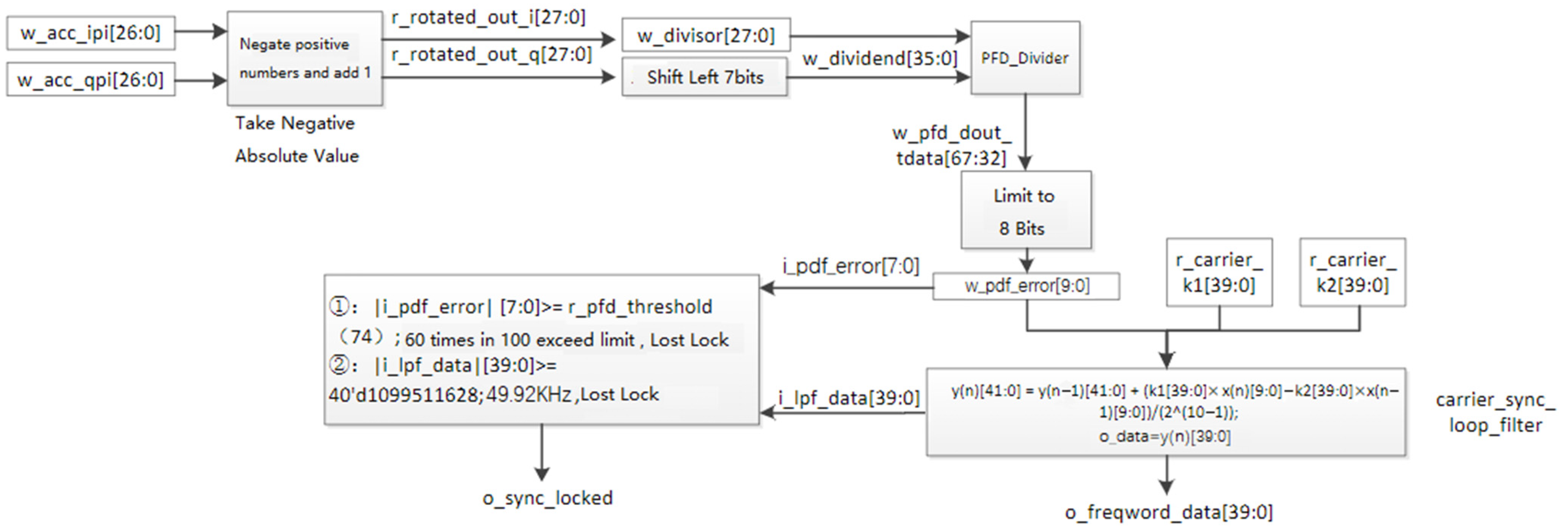
3.3. FFT Fast Acquisition Method Introducing Bit Synchronization Loop

The pseudo-code rate of Beidou B2a and B3I signals is 10.23 Mcps, and the pseudo-code period before scrambling is 1023, so one pseudo-code period is 100 μs. The symbol rate is variable from 2 K to 256 Kbps [7,8,38,39,40,41,42,43], which poses a huge problem for fast acquisition algorithms that information symbol rates must be an integral multiple of the pseudo-code rate. How to achieve high real-time and high sensitivity acquisition requirements and how to solve the problem of aligning the symbol rate and spreading code during acquisition is of great research significance. If the acquisition module of the front spreading code avoids the problem of misalignment between the symbol rate and the spreading code, in exchange for reducing the calculation time cost, this problem needs to be solved in the tracking module [44,45,46,47,48]. The time domain parallel frequency domain FFT fast acquisition method (hereinafter referred to as “FFT fast acquisition method”) can be implemented on the Xilinx corporation’s (San Jose, CA, USA) Zynq 7030 chip using only 40% of the logic resources. The simulation parameters are compared using the FFT frequency domain acquisition method and the FFT fast acquisition method when doing 256-point FFT. The results of the comparison and the simulation analysis are shown in Table 1 [8,42].
Based on the above analysis, this design proposes the FFT fast acquisition method that combines the time domain and frequency domain, which can achieve signal acquisition without aligning the symbol rate with the spreading code [47,48,49]. This design plans to use a Zynq 7030 chip as the basis of the signal capture module. With its low cost and small size, it can fully meet the resource implementation of fast acquisition algorithms [44,46,50].
The FPGA design diagram of the fast acquisition algorithm is shown in Figure 6. The beam-synthesized data are sent to the data buffer, then sent to 64 parallel correlators in parallel. The correlation results are sent to the buffer. The correlation length of each correlator is dynamically configurable and can support a minimum of 16 chip periods, thereby supporting a maximum symbol rate of 256 Kbps and a maximum Doppler frequency shift of 250 kHz. The length of the 64 buffers is 512, thus supporting coherent accumulation of four pseudo-code periods. Considering the spectrum leakage problem of FFT, it can obtain a gain of approximately 4.7 dB. After the correlation results are buffered, the FFT executes a 256-point complex FFT, performs a frequency domain search, calculates the SNR, and determines whether the threshold is reached. When the threshold is exceeded, the code phase and Doppler value at that moment are recorded and sent to the subsequent tracking module [51,52,53,54].
To complete the search for the entire code phase, more than 1023 × 2/64 = 32 operations are required. Each correlation time is four pseudo-code periods. Therefore, the search and acquisition time to complete one code period is 128 pseudo-code periods, which is approximately 12.8 ms. In order to speed up the calculation time of FFT, this solution uses two 256-point complex FFTs executed in parallel, and the actual capture time is measured to be 32.8 ms [47,48,49,54,55].
In order to solve the demodulation problem when the information symbol rate is not an integer multiple of the pseudo-code rate, the tracking module needs to introduce a third loop, named a bit synchronization loop, to achieve tracking and demodulation of signals containing large Doppler shift and pseudo-code asynchronous signals in satellite downlink signals [47,48]. In this scheme, the carrier loop uses the COSTAS loop, the pseudo-code loop uses the DDLL loop, and the bit synchronization loop uses the classic DTTL loop [56].
The detailed design of the three loops of the tracking module is shown in Figure 7, Figure 8 and Figure 9, respectively. It includes (1) three DDSs, which drive the carrier tracking loop, the pseudo-code tracking loop, and the bit synchronization tracking loop, respectively; (2) lead-lag timely correlators, of which there are four in parallel, which correlate different code phases to support RAKE reception; (3) pseudo-code phase error detection, carrier and phase error detection, SNR estimator, and data edge jump detector; (4) three LPF low-pass filters to track Doppler and Doppler acceleration.
The precise tracking of the code chip is divided into two steps: (1) First, the code chip tracking loop uses the non-coherent envelope correlation delay lock loop to perform a rough measurement of the code chip delay. Under the premise of ensuring the normal tracking of the code delay lock loop, the narrowest possible correlation interval is used, and the accuracy of the code chip delay estimation is limited to one code chip; (2) Then, the carrier-assisted technology is used to estimate the carrier phase through the detection algorithm, and the change value of this carrier phase in the code delay lock loop data update interval (also called differential phase) is fed back to the digital control oscillator of the code loop, and the code delay offset caused by the Doppler effect is corrected by fine-tuning the code NCO. On the basis of ensuring the reliable tracking of the code delay lock loop, a narrow loop bandwidth, and a smaller correlation interval are used to obtain the required accurate code chip delay estimation value.
This system uses carrier-assisted technology, that is, the carrier phase change is used to assist the code delay loop in tracking. Because the noise that causes carrier loop jitter is much smaller than the noise that causes code loop jitter, appropriate signal estimation technology can be used in highly dynamic environments. While the carrier tracking loop accurately tracks the carrier phase change, it can extract accurate chip delay correction to assist the code delay loop in tracking. If the chip delay change is continuous, the bandwidth of the DDLL loop can be made very narrow to suppress noise. The essence of this method is that the carrier tracking loop provides accurate chip delay changes, and the code tracking loop DDLL improves the measurement accuracy of chip delay by adopting a narrower loop bandwidth and a smaller correlation interval.
The state transition diagram of the capture and tracking module is shown in Figure 10.
After the signal is captured and tracked stably, the signal needs to be decoded, which requires steps such as (2, 1, 7) Viterbi decoding, differential decoding, parallel-to-serial conversion, frame header search, descrambling, deinterleaving to form four 255-byte data block, RS decoding, and uploading to the host computer [44]. The FPGA design of the decoding module is shown in Figure 11. Among them, the design of the VTB relay code, descrambling, and deinterleaving are all using IP cores.

3.4. Overall Machine Design

As introduced before, according to the independence of functions of each part in the low-orbit satellite signal on-board and ground data processing processes, the system can be divided into four parts: antenna array, radio frequency unit, baseband processing board, and application processing terminal.
Among them, the antenna array consists of 31 identical antenna elements. The antenna elements adopt a circular polarization method and support receiving left-hand circular polarization and right-hand circular polarization signals at the same time. The left-hand and right-hand circular polarization signals are filtered separately. After amplification, the combined signal is transmitted to the RF local oscillator board through the RF cable. The left-hand RF frequency point, which is 2860 MHz, has a close frequency with the right-hand RF frequency point, which is 2074 MHz, so the left-hand channel and the right-hand channel adopt the same design [57]. The left-handed signal is mixed in the form of LO-RF, and the right-handed signal is mixed in the form of RF-LO, which widens the frequency spacing of the left/right-hand local oscillators. The left-handed local oscillator frequency is designed to be 2860 MHz, and the corresponding left-handed intermediate frequency is 376~480 MHz, which is located in the second Nyquist zone of the ADC. The right-handed local oscillator frequency is designed to be 2074 MHz, and the corresponding right-handed intermediate frequency is 126~230 MHz, which is located in the first Nyquist zone of the ADC. Figure 12 shows the spectrum after mixing.
The left/right-handed local oscillator will leak, resulting in mutual modulation. The modulated signal is 786 MHz, which can be filtered out using a low-order low-pass filter. After the intermediate frequency signal obtained after mixing is sampled by the ADC, the spectrum of the second Nyquist zone will be moved to the first Nyquist zone. Figure 13 shows the spectrum after ADC sampling.
As can be seen from Figure 1, the sampled signal does not undergo aliasing, so it will not cause a loss in signal-to-noise ratio.
The RF unit mainly consists of three circuits, namely a down-conversion and intermediate frequency amplification circuit, a local oscillator generation circuit, and a power supply circuit [44]. There are 32 down-conversion channels, corresponding to 31 antenna array elements, and the remaining 1 down-conversion channel is reserved; the baseband processing board is mainly responsible for processing the 200 MHz bandwidth intermediate frequency signal transmitted from the down-conversion board, and after AD conversion, each signal is sent to the FPGA for beamforming separately and then sent to the subsequent SoC for signal demodulation and decoding, the SoC uses the Zynq 7030 chip. The schematic diagram of data flow is shown in Figure 14. The decoded baseband data are sent to the host computer through 1 Gigabit Ethernet. The data processing terminal, that is, the host computer, is mainly responsible for receiving target detection data, radar and communication data, image slices, vector data, digital elevation maps, and satellite real-time orbit data, in the meantime issuing control and management instructions to the receiver, and interact with receiver [44].
The SoC baseband board mainly implements digital beam synthesis, anti-interference processing, signal acquisition, tracking, and decoding, and uses a board-to-board high-speed connector to connect the baseband board and the multi-channel down-conversion board. The 32 channels of intermediate frequency signals are sent to the 32 channels of ADC for analog-to-digital conversion, and then the digital signals are sent to the beam steering FPGA. The beam steering FPGA uses Fudan Microelectronics’ JFM7K325T (K7 for short) chip which contains a large number of DSP units inside the chip. The DSP unit is mainly used for digital down-conversion and phase-shifting processes of multi-beams, narrow-band anti-interference, etc. [44]. The synthesized beams complete narrow-band anti-interference inside the FPGA. After processing, it is sent to the baseband processing FPGA. The chip contains a large number of logic resources, which is sufficient for multi-channel capture, tracking, and decoding processes. The schematic block diagram of the baseband processing board is shown in Figure 15.

4. Simulation Results

4.1. RF Link Simulation and Budgeting

This scheme uses ADS 2020 software to design the gain of the RF circuit and estimate the noise figure, InP1dB, and IIP3 values. Considering that if the received signal is required to have an anti-interference signal-to-interference ratio of >45 dB, the power range of the satellite signal reaching the ground is −127~−115 dBm, that is, the receiver can resist interference of −70 dBm (−115 dBm + 45 dB). In this case, the receiver is required not to be saturated due to the interference signal. The saturated input power of a typical high-speed ADC is about 2 dBm; the receiver’s in-band (200 MHz) thermal noise is about −90 dBm, and the amplified thermal noise is required to be greater than the quantization noise of the ADC. Based on the above two points, it is reasonable to set the receiver’s amplification factor to 55 dB. According to the above analysis, the simulation of the RF link is shown in Figure 16.
The link budget results are shown in Figure 17.
The budget result of the RF link shows that the link gain is approximately 56.7 dB. The noise coefficient of all LNAs in this RF link is usually between 1 dB and 2 dB. Assuming that all noise in the RF link is introduced by LNA, here we assume that the noise of the RF link is 1.5 dB. The RF circuit output thermal noise is approximately −37.2 dBm, the input 1 dB gain compression point is approximately −36.5 dBm, and the input third-order intermodulation cutoff point is about −20 dBm.

4.2. Digital Beamforming Simulation

This scheme uses HFSS 15.0 software to simulate the digital beamforming module. The Digital Beamforming system (hereinafter referred to as “DBF system”) generates variable beams by controlling the phase and amplitude of each element signal of the array antenna through data technology. Therefore, the beamforming problem is mainly to determine the amplitude and phase weighting coefficients of each element signal required in different directions. In engineering implementation, there are two main ways to generate weighting coefficients for beamforming: real-time calculation of weighting coefficients and look-up table calculation. The real-time calculation method is to use an adaptive algorithm to adjust the weighting coefficients based on certain decision criteria (such as detecting the signal power after beamforming). The advantage of this method is that it adjusts the weighting coefficients in real-time according to the characteristics of the synthesized signal, suppresses the sidelobes, and optimizes the received signal. It can adapt to different application environments in real-time. The disadvantage is that the calculation amount is large, and the hardware platform and algorithm optimization requirements are high. The look-up table method calculates the weighting coefficients of different directions through simulation analysis and solidifies the coefficients in the memory. The weighting coefficients of the corresponding direction are extracted according to the specific pointing parameters for beam synthesis. The advantages of this method are small calculation amounts, fast running speed, and simple algorithm design. The disadvantage is that the weighting coefficients cannot be adjusted in real time and the adaptability to interference signals is poor. Considering that the communication time of low-orbit satellites is short each time and the beam changes quickly, this scheme adopts the look-up table method.
In this scheme, Taylor distribution or Chebyshev distribution is used to optimize the amplitude weighting of each unit of the beam to achieve the low sidelobe characteristics of the array beam and at the same time reduce the beam gain, taking both low sidelobe and constant gain performance into account. Table 2 shows the gains and sidelobe levels of several typical directional beams after optimization. In these angles, the sidelobe level decreases by 1 to 8 dB. In the entire three-dimensional beam space, the gain is within 14 to 15 dBic, and the sidelobe levels are lower than −11 dB.
Figure 18 and Figure 19 show the beam characteristic diagrams of (θ, φ) = (0°, 0°) and (θ, φ) = (0°, 45°) before and after optimization, respectively. Due to space limitations, the beam characteristic diagrams of other angles before and after optimization are not listed here.
As can be seen from Figure 18, before optimization, at the desired signal direction φ = 0°, the mainboard signal strength is 15.3 dBic, and there is a sidelobe with a strength of 1 dBic at ±35° and ±80°, and nulls are formed in the remaining directions. Since the sidelobe sizes in the four directions are all greater than 0 dBic and the energy is strong, the beamforming effect is not so good; after using Taylor distribution to optimize the beamforming directivity diagram, the main lobe at the desired direction φ = 0° is slightly weakened, from the original 15.3 dBic to 15.0 dBic, but the sidelobes at ±35° are well suppressed to form nulls, and the sidelobes at ±80° are also well suppressed, with the strength reduced from 1 dBic to −5 dBic. It can be seen that the use of Taylor distribution can improve the beamforming directivity diagram to a certain extent.
Similarly, it can be seen from Figure 19 that before optimization, for the directivity diagram at the desired direction of φ = 45°, the signal strength in the main lobe direction is 13dBic, and there is a sidelobe with an intensity greater than 0dBic in the 0° and 90° directions, and no null is formed well in other directions, and the sidelobe energy is strong; after optimization using the Chebyshev distribution, although the main lobe is slightly weakened compared to before optimization, the energy drops from the original 13 dBic to 10 dBic, but nulls can be well-formed in other sidelobe directions, and the sidelobe energy is greatly weakened compared to before optimization. It can be seen that the use of Chebyshev distribution can improve the directivity diagram of beamforming to a certain extent.

4.3. Time–Frequency Domain Narrowband Anti-Interference Simulation

This scheme uses Matlab 2017 software to simulate the module of counteracting narrowband interference. Four array antennas were used to conduct an anti-narrowband interference simulation test on the BD2 B3 signal (operating frequency is 1268.52 MHz ± 10.23 MHz). The signal amplitude of the generated narrowband interference signal is -70dBm. The simulation results of anti-single-band narrowband interference and anti-three-band narrowband interference are shown in Figure 20. The test results show that when receiving the B3 frequency point, the receiver can resist up to three narrowband interferences at the same time; when resisting interference from a single frequency band and three frequency bands, the interference-to-signal ratio is ≥57 dB and ≥47 dB, respectively (signal level −133 dBm). Among them, the real-time performance of interference suppression is better than 1ms.

4.4. Capture and Tracking Module Simulation

This scheme uses Matlab 2017 software to simulate the module of capture and tracking. The simulation parameters of the capture and tracking module are shown in Table 3. The simulation result of the capture module is shown in Figure 21.
The simulation results of the carrier loop and code loop are shown in Figure 22.
The simulation results of the bit synchronization loop are shown in Figure 23 and Figure 24.
The simulation results show: (1) In a large dynamic scenario, the bit synchronization loop can complete bit synchronization within 60 ms, and the sampling point can be adjusted in real-time during operation. The loop works normally, the mean estimation error is <8.7, and the standard deviation of the estimation error is <7.5; (2) A signal with a carrier-to-noise ratio of 44 dBHz runs at a rate of 8 ksps for 100 s, and the bit error rate is 0.
The above simulation results verify the effectiveness and correctness of the algorithm. The algorithm consumes fewer resources compared to the traditional FFT frequency domain acquisition method and is easy to engineer by implementing software engineering through the JFM7K325T chip.

4.5. VTB Decoding Simulation

This scheme uses Matlab 2017 software to simulate the module of VTB decoding. The relationship curve between the Viterbi decoding bit error rate and the normalized signal-to-noise ratio is shown in Figure 25.
It can be concluded from the figure that when the bit error rate is 10−3, 10−5, and 10−7, respectively, the Eb/N0 and decision gain are as shown in Table 4.
It can be concluded from the reams of evidence above: (1) For (2, 1, 7) convolutional codes, when the free distance is 10, the upper bound of the coding gain is 7dB; (2) The coding gain increases as the bit error rate decreases, but it will not rise infinitely.

5. Conclusions and Future Work

This solution combines digital beamforming technology, time–frequency domain interference suppression technology, three-loop capture and tracking technology that introduces a bit synchronization loop, and RS decoding and other technologies based on FPGA digital processing board, using the JFM7K325T chip to design the FPGA, which is designed by Fudan Microelectronics and contains a large number of DSP units, which are mainly used for multi-beam digital down-conversion and phase shift processing, narrow-band anti-interference, etc. And use the JFM7K325T chip to perform simulation design of the whole low-orbit satellite broadcast signal receiving and processing terminal. The simulation results show that the beamforming gain of the whole machine reaches 14–15 dBic; the interference-to-signal ratio reaches 57 dB when resisting interference from a single frequency band, and the interference-to-signal ratio reaches 47 dB when resisting interference from three frequency bands; in large dynamic scenarios, the bit synchronization loop can complete bit synchronization within 60 ms, with a bit error rate of 0; the coding gain can reach 7 dB.
The low-orbit satellite broadcast signal processing terminal designed in this scheme still has room for improvement: 1. Currently, the three channels of a single frequency point have occupied about 85% of the FPGA logic resources, which is close to saturation. In the future, the process of capture, tracking, and decoding will be considered for transplanting to the ARM part. In this case, the SoC can replace the Z7030 chip with the Z7045 chip with larger logical resources to improve the computing speed and processing capabilities of the entire machine; 2. The algorithm of the bit synchronization loop can continue to be improved, reducing the time required for bit synchronization in large dynamic scenarios.

Author Contributions

Literature search: H.S. and J.L.; Theoretical methods: H.S. and J.L.; Software design: J.L. and Z.W.; Graph creation: H.S. and Z.W.; Data collection: J.L. and Z.W.; Data analysis: H.S. and Z.W.; Writing—original draft: H.S.; Writing—review & editing: J.L. and Z.W.; Supervision and guidance: J.L. All authors have read and agreed to the published version of the manuscript.

Funding

This work was funded by Shandong Provincial Natural Science Foundation (ZR2021MD127), research on multi-source information fusion and high-precision positioning technology in complex environments.

Data Availability Statement

Data is contained within the article.

Conflicts of Interest

The authors declare no conflict of interest.

References

  1. Zhou, J.; Sun, Z.; Zhang, R.; Lin, G.; Zhang, S.; Zhao, Y. A Cloud-Edge Collaboration CNN-Based Routing Method for ISAC in LEO Satellite Networks. In Proceedings of the 2nd Workshop on Integrated Sensing and Communications for Metaverse, Helsinki, Finland, 18 June 2023. [Google Scholar]
  2. Wang, C.; Wang, Z. Improved Acquisition Method of GPS Signal by Wavelet De-noising. In Proceedings of the International Conference on Industrial Technology and Management Science(ITMS 2015), Tianjin, China, 27–28 March 2015. [Google Scholar]
  3. Sun, Y.; Peng, M.; Zhang, S.; Lin, G.; Zhang, P. Integrated Satellite-Terristrial Networks: Architectures, Key Techniques, and Experimental Progress. IEEE Netw. 2022, 36, 191–198. [Google Scholar] [CrossRef]
  4. Cong, M. Research of Narrowband Anti-Interference Technologies in Satellite Navigation. Master’s Thesis, Beijing Institute of Technology, Beijing, China, 2016. [Google Scholar]
  5. Feng, H. Research on Estimation of ISAR Amplitude-Phase Error in Pulses and Narrow-Band Interference for Waveform Optimization Method. Master’s Thesis, Xidian University, Xi’an, China, 2022. [Google Scholar]
  6. Liu, J.; Du, X.; Cui, J.; Pan, M.; Wei, D. Task-Oriented Intelligent Networking Architecture for the Space-Air-Ground Aqua Integrated Network. IEEE Internet Things J. 2020, 7, 5345–5358. [Google Scholar] [CrossRef]
  7. Qian, Z. Complex Electromagnetic Signal Acquisition Technology Based on Radio Frequency Identification of Internet of Things. In Proceedings of the 2020 International Conference on Computer Information and Big Data Applications (CIBDA), Guiyang, China, 17–19 April 2020. [Google Scholar]
  8. Xu, W. Research on the Fast Acquisition Method of Beidou Satellite Signals. Master’s Thesis, Southeast University, Nanjing, China, 2022. [Google Scholar]
  9. Fenech, H.; Amo, S. The Role of Array Antennas in Commercial Telecommunication Satellites. In Proceedings of the 2016 10th European Conference on Antennas and Propagation (EuCAP), Davos, Switzerland, 10–15 April 2016; IEEE: New York, NY, USA, 2016. [Google Scholar]
  10. Gordana, B.; Marius, O.; Florin, A.; Ana, G. Digital Beamforming Techniques for Future Communications Systems. In Proceedings of the 2020 12th International Symposium on Communication Systems, Networks and Digital Signal Processing (CSNDSP), Porto, Portugal, 20–22 July 2020. [Google Scholar]
  11. Staileyand, J.E.; Hondl, K.D. Multifunction Phased Array Radar for Aircraft and Weather Surveillance. Proc. IEEE 2016, 104, 649–659. [Google Scholar] [CrossRef]
  12. Zhang, Q.; Feng, S.; Fu, L.; Wen, J.; Ge, J.; Ma, J. Design and Implementation of Adaptive Digital Beamforming Based on FPGA. In Proceedings of the 2023 4th China International SAR Symposium (CISS), Xi’an, China, 4–6 December 2023; IEEE: New York, NY, USA, 2023. [Google Scholar]
  13. Rui, C.; Xiaohui, T.; Lihui, J.; Zhang, J.; Peng, G.; Rong, D.; Xu, X.; Zhang, Y.; Xu, Y.; Yang, H. A Wideband Digital Beamforming System for Large Aperture Array Radio Telescope. In Proceedings of the 2022 Asia-Pacific Microwave Conference (APMC), Yokohama, Japan, 29 November–2 December 2022. [Google Scholar]
  14. Zhang, B.; Liu, H.; Zhai, G.; Meng, M. Comparative study on adaptive digital beamforming techniques. In Proceedings of the 2024 IEEE 6th Advanced Information Management, Communicates, Electronic and Automation Control Conference (IMCEC), Chongqing, China, 24–26 May 2024. [Google Scholar]
  15. Spoof, K.; Tenhunen, M.; Unnikrishnan, V.; Stadius, K.; Kosunen, M.; Ryynänen, J. True-Time-Delay Receiver IC With Reconfigurable Analog and Digital Beamforming. IEEE Access 2022, 10, 116375–116383. [Google Scholar] [CrossRef]
  16. Dusari, N.R.; Shipra, M.R. Digital Beamforming with Digital Predistortion using Xilinx RF SoC ZCU216. In Proceedings of the 2022 IEEE International Conference on Signal Processing and Communications (SPCOM), Bangalore, India, 11–15 July 2022. [Google Scholar]
  17. Li, Y.; He, S.; Ma, C.; Ma, S.; Li, C.; Yang, L. Channel Characteristic and Capacity Analysis of Millimeter Wave MIMO Beamforming System. In Proceedings of the 2016 IEEE 83rd Vehicular Technology Conference (VTC Spring), Nanjing, China, 15–18 May 2016. [Google Scholar]
  18. Subramaniyan, E.; Rajagopal, S. Wideband Beamforming using Digital Phase Only Compensation in Digital Array Radars. In Proceedings of the 2022 IEEE International Conference on Electronics, Computing and Communication Technologies (CONECCT), Bangalore, India, 8–10 July 2022. [Google Scholar]
  19. Liang, Y.; Xu, A.; Zhang, M.; Zhai, H.; Yuan, H. Research and Realization of Adaptive Digital Beamforming Technology Based on Spatial Spectrum Estimation. In Proceedings of the 2021 CIE International Conference on Radar (Radar), Haikou, China, 15–19 December 2021. [Google Scholar]
  20. Chen, Y.; Wang, D.; Liu, P.; Xu, Z.; Wei, C.; Dong, Q. An improved approach of SFAP algorithm for suppressing concurrent narrow and wide band interference. In Proceedings of the 7th Satellite Navigation Conference, Shanghai, China, 18–20 May 2016. [Google Scholar]
  21. Akho-Zahieh, M.M.; Abdellatif, N. Narrow-band Interference Suppression in Wavelet Packet Multirate Multicarrier CDMA System. In Proceedings of the 2nd International Conference on Communication Technology (ICCT 2015), Hangzhou, China, 18–20 October 2015. [Google Scholar]
  22. Lu, R.; Weston, C.; Weyer, D.; Buhler, F.; Lambalot, D.; Flynn, M.P. A 16-Element Fully Integrated 28-GHz Digital RX Beamforming Receiver. IEEE J. Solid State Circuits 2021, 56, 1374–1386. [Google Scholar] [CrossRef]
  23. Yao, R.; Chen, Y.; Li, G.; Feng, Z.; Wang, L. Iterative Threshold Algorithm for Narrow-band Interference Suppression. In Proceedings of the 2013 22nd Wireless and Optical Communication Conference, Chongqing, China, 16–18 May 2013. [Google Scholar]
  24. Cui, X.; Liu, Y.; Wei, W.; Liao, K.; Yu, D. An Improved Narrow-Band Interference Suppression Method for HINOC System. In Proceedings of the 2012 IEEE 11th International Conference on Solid-State and Integrated Circuit Technology(ICSICT-2012), Xi’an, China, 29 October–1 November 2012. [Google Scholar]
  25. Lyn, Q.S.; Qzin, H.L. A General Method to Mitigate the ContinuousWave Interference and Narrowband Interference for GNSS Receivers. IET Radar Sonar Navigation 2020, 14, 1430–1435. [Google Scholar]
  26. Huang, L.; Lu, Z.K.; Xiao, Z.; Ren, C.; Song, J.; Li, B. Suppression of Jammer Multipath in GNSS Antenna Array Receiver. Remote Sens. 2022, 14, 350. [Google Scholar] [CrossRef]
  27. Chen, C.; Zhuo, Y. A research on anti-jamming method based on compressive sensing for OFDM analogous system. In Proceedings of the 2017 IEEE 17th International Conference on Communication Technology (ICCT), Chengdu, China, 27–30 October 2017. [Google Scholar]
  28. Chen, Q.; Liang, J.; Zhang, F.; Bi, B. Research on Anti-jamming Algorithm of BDS Signal in WiFi6 Environment. In Proceedings of the 2020 IEEE 8th International Conference on Information, Communication and Networks (ICICN), Xi’an, China, 22–25 August 2020. [Google Scholar]
  29. Issam, S.M.; Adname, A.; Madiabdessalam, A. Anti-Jamming Techniques for Aviation GNSS-based Navigation systems: Survey. In Proceedings of the IEEE 2nd International Conference on Electronics, Control, Optimization and Computer Science, Kenitra, Morocco, 2–3 December 2020. [Google Scholar]
  30. Hao, Z.H.; Zhao, H.Z.; Shao, S.H.; Tang, Y. Suppression of Time-Varying Multi-Tone Interference Based on Frenquency Domain Interference Detection. Wirel. Pers. Commun. 2014, 75, 1051–1060. [Google Scholar] [CrossRef]
  31. Wei, D.; Cui, J.; Niu, L.; Zhang, R.; Hou, C. Research on Anti-interference Algorithm Based on FFT-Wavelet Threshold. In Proceedings of the 2020 7th International Forum on Electrical Engineering and Automation (IFEEA), Hefei, China, 25–27 September 2020. [Google Scholar]
  32. Han, Y.; Zhang, M.; Shen, L.; Wang, L. The Anti-Interference Algorithm of BPSK Spread Spectrum Signal Based on Generative Adversarial Networks. In Proceedings of the 2022 7th International Conference on Signal and Image Processing (ICSIP), Suzhou, China, 20–22 July 2022. [Google Scholar]
  33. Li, H.; Huo, Q.; Zheng, X.; Yan, S.; He, Y. High Dynamic GNSS Anti-Jamming Algorithms Based on Nuffling Widening and Depening. In Proceedings of the IEEE 4th Information Technology, Networking, Electronic and Automation Control Conference, Chongqing, China, 12–14 June 2020. [Google Scholar]
  34. Jianhua, C.; Naiping, C.; Panfeng, H. Adaptive anti jamming algorithm for GNSS software receiver. In Proceedings of the 2016 IEEE Information Technology, Networking, Electronic and Automation Control Conference, Chongqing, China, 20–22 May 2016. [Google Scholar]
  35. Zhong, W. Linear phase FIR Digital Filter Design Using Differential Evolution Algorithms. Master’s Thesis, University of Windsor, Windsor, ON, Canada, 2017. [Google Scholar]
  36. Guan, W.; Zheng, Z.; Chang, S.; Liu, Q.; Chen, X. A frequency-domain sparse multi-functional anti-jamming waveform design and processing method. In Proceedings of the IET International Radar Conference (IRC 2023), Chongqing, China, 3–5 December 2023. [Google Scholar]
  37. Ramanathan, R.; Soman, K.P.; Vidyapeetham, A. A Novel Methodology for Designing Linear Phase IIR Filters. Int. J. Recent Trends Eng. 2009, 1, 218. [Google Scholar]
  38. Kai, Z. Research on Fast Acquisition Method of High Dynamic Signals. Master’s Thesis, Xidian University, Xi’an, China, 2014. [Google Scholar]
  39. Cristallini, D.; Blazquez-Garcia, R.; Daniel, O’Hagan. K-space signal occupancy of Starlink signals and their applications in passive radar imaging. In Proceedings of the 2023 IEEE Radar Conference (RadarConf23), San Antonio, TX, USA, 1–5 May 2023. [Google Scholar]
  40. Jianjian, Y.; Ren, G.; Xuguo, Z. Frequency Domain Parallel Acquisition Algorithm Based on FFT. Comput. Eng. Appl. 2012, 48, 250–252. [Google Scholar]
  41. Jiao, X.; Wang, J.; Li, X. High Sensitivity GPS Acquisition Algorithm Based on Code Doppler Compensation. In Proceedings of the 2012 IEEE 11th International Conference on Signal Processing (ICSP 2012), Beijing, China, 21–25 October 2012. [Google Scholar]
  42. Zhou, C.; Wu, Z.; Cao, Y.; Xu, J.; Zhang, L.; Yang, L.; Guo, W. A novel unsupervised anti-intermittent sampling jamming method for intra-pulse and inter-pulse frequency agile radar. In Proceedings of the IET International Radar Conference (IRC 2023), Chongqing, China, 3–5 December 2023. [Google Scholar]
  43. Qiu, L.; Fan, Y. Smart Noise Jamming Suppression Method Based on Target Position Estimation. In Proceedings of the 2022 3rd International Conference on Computer Vision, Image and Deep Learning & International Conference on Computer Engineering and Applications (CVIDL & ICCEA), Changchun, China, 20–22 May 2022. [Google Scholar]
  44. Gang, X. Principles of GPS and Receiver Design; Publishing House of Electronics Industry: Beijing, China, 2009; p. 262. [Google Scholar]
  45. Yiming, F. A Survey on Low Earth Orbit Satellite Signal Acquisition and Tracking Technology. Radio Commun. Technol. 2023, 49, 816–825. [Google Scholar]
  46. Xunxiong, H. Research on Key Technologies of Beidou Third Generation Multifrequency Point Satellite Signal Acquisiton. Master’s Thesis, Guilin University of Electronic Technology, Guilin, China, 2022. [Google Scholar]
  47. Bhatt, H.S.; Garg, G. Comparative analysis of acquisition methods in digital forensics. In Proceedings of the 2021 Fourth International Conference on Computational Intelligence and Communication Technologies (CCICT), Sonepat, India, 3 July 2021. [Google Scholar]
  48. Kalita, S.; Kaushik, R.; Jajoo, M.; Sahu, P.P. Performance Enhancement of a Multichannel Uncoordinated Code Hopping DSSS Signaling Scheme Using Multipath Fading Compensator. J. Circuits Syst. Comput. 2016, 25, 1650145. [Google Scholar] [CrossRef]
  49. Cui, H.; Li, Z.; Dou, Z. Fast Acquisition Method of GPS Signal Based on FFT Cyclic Correlation. In Proceedings of the 13th International Conference on Wireless Communications, Networking and Mobile Computing (WiCOM 2017), Guilin, China, 21–23 August 2017. [Google Scholar]
  50. Guangyue, D.; Meili, L.; Feng’e, Y.; Xiaohong, W.; Xiaomeng, D.; Benlan, S. Study on synchronous method of multi-sensor data acquisition in space based on Single-bus digital temperature sensor. In Proceedings of the 2022 International Conference on Advanced Mechatronic Systems (ICAMechS), Toyama, Japan, 17–20 December 2022. [Google Scholar]
  51. Jiang, H.; Li, J.; Zhu, X.; Ou, G. Design and Validation of A Single Frequency GPS Software Receiver Acquisition and Tracking Method. In Proceedings of the 2017 IEEE 2nd Advanced Information Technology, Electronic and Automation Control Conference (IAEAC 2017), Chongqing, China, 25–26 March 2017. [Google Scholar]
  52. Zhang, S.; Wan, G.; Wang, S. 2017 IEEE 17th International Conference on Communication Technology (ICCT). In Proceedings of the 2023 3rd Asia-Pacific Conference on Communications Technology and Computer Science (ACCTCS), Shenyang, China, 25–27 February 2023. [Google Scholar]
  53. Lee, S.; Yoon, J.; Kang, S. Giga-sample Data Acquisition Method for High-speed DDR5 SDRAM. In Proceedings of the 2021 18th International SoC Design Conference (ISOCC), Jeju Island, Republic of Korea, 6–9 October 2021. [Google Scholar]
  54. Zhang, S.; Dai, Z.; He, H.; Zhang, W.; Liu, N.; Shi, C. A Study on One Fast Acquisition Method for DS/FH Hybrid Spread Spectrum Signal in Physical Layer of Aircraft Communication Network. In Proceedings of the 2022 International Symposium on Networks, Computers and Communications (ISNCC), Shenzhen, China, 19–22 July 2022. [Google Scholar]
  55. Pan, Y.; Zhang, T.; Zhang, G.; Luo, Z. A Novel Acquisition Algorithm Based on PMF-apFFT for BOC Modulated Signals. IEEE Access 2019, 7, 46686–46694. [Google Scholar] [CrossRef]
  56. Li, X.; Yingnan, C.; Bin, G. The Research on GPS Signal Acquisition Algorithm Based on Coherent Integration. In Proceedings of the 2020 39th Chinese Control Conference (CCC), Shenyang, China, 27–29 July 2020. [Google Scholar]
  57. Kai, C. RF and Microwave Wireless Systems; John Wiley & Sons: New York, NY, USA, 2004. [Google Scholar]
Figure 1. Complete data processing flow chart of low-orbit satellite signals on the satellite and on the ground.
Electronics 13 03270 g001
Figure 2. Processing flow chart of ground receiving terminal.
Electronics 13 03270 g002
Figure 3. Schematic diagram of sub-system relationships.
Electronics 13 03270 g003
Figure 4. Digital beamforming principal diagram.
Electronics 13 03270 g004
Figure 5. Implementation block diagram of time–frequency domain notch technology based on FFT.
Electronics 13 03270 g005
Figure 6. Fast acquisition algorithm FPGA design diagram.
Electronics 13 03270 g006
Figure 7. FPGA design of carrier tracking loop.
Electronics 13 03270 g007
Figure 8. FPGA design of code tracking loop.
Electronics 13 03270 g008
Figure 9. FPGA design of data tracking loop.
Electronics 13 03270 g009
Figure 10. Capture and tracking module state transition diagram.
Electronics 13 03270 g010
Figure 11. Decoding module flow chart.
Electronics 13 03270 g011
Figure 12. The spectrum after mixing.
Electronics 13 03270 g012
Figure 13. The spectrum after ADC sampling.
Electronics 13 03270 g013
Figure 14. Schematic diagram of data flow between FPGA and SoC on the baseband processing board.
Electronics 13 03270 g014
Figure 15. Principal block diagram of baseband processing board.
Electronics 13 03270 g015
Figure 16. Simulation link of RF channel.
Electronics 13 03270 g016
Figure 17. RF link budget results.
Electronics 13 03270 g017
Figure 18. The (θ, φ) = (0°, 0°) beam characteristics before and after optimization.
Electronics 13 03270 g018
Figure 19. The (θ, φ) = (0°, 45°) beam characteristics before and after optimization.
Electronics 13 03270 g019
Figure 20. (a) Schematic diagram of the interference-to-signal ratio of the received signal in anti-single-band narrowband interference test; (b) schematic diagram of the interference-to-signal ratio of the received signal with frequency in three-band narrowband interference test.
Electronics 13 03270 g020
Figure 21. Ratio of maximum and average values of coherence results.
Electronics 13 03270 g021
Figure 22. (a) PLL phase detector phase difference and PLL Doppler; (b) DLL phase detector phase difference and Doppler; (c) 1ms accumulator output; (d) tracking carrier-to-noise ratio.
Electronics 13 03270 g022aElectronics 13 03270 g022b
Figure 23. Bit synchronization ring operation results: (a) estimated data code position offset; (b) actual data code position offset; (c) data code position estimation error.
Electronics 13 03270 g023aElectronics 13 03270 g023b
Figure 24. Bit error rate changes over time.
Electronics 13 03270 g024
Figure 25. Relationship curve between bit error rate and normalized signal-to-noise ratio.
Electronics 13 03270 g025
Table 1. Comparison results between FFT fast acquisition method and traditional FFT frequency domain capture method.
Compared ItemsFFT Frequency Domain Acquisition MethodFFT Fast Acquisition Method
Symbol rateCan only be an integer multiple of the pseudocode periodArbitrary proportional relationship
Pseudocode and symbol alignmentNecessaryUnnecessary
Accumulation methodIncoherentCoherent
Cumulative lengthGenerally, 4 cycles4~8 cycles
Maximum value of Doppler frequency±100 kHz±250 kHz
Capture timeAbout 1 sAbout 60 ms
Table 2. Sidelobe level reduction and gain of several typical beam angles after optimization (G/T value is −9 dB/K).
Beam Pointing Angle (θ, φ)Sidelobe Level Reduction (dB)Gain (dBic)
(0°, 0°)515.00
(20°, 0°)814.60
(45°, 0°)314.89
(65°, 0°)314.97
(75°, 0°)714.63
(75°, 30°)4.514.30
(75°, 60°)114.57
(75°, 90°)2.514.73
(75°, 120°)214.71
(75°, 150°)214.94
(75°, 180°)114.92
Table 3. Capture and tracking module simulation parameters.
Simulation ParametersValue
Signal
Parameters
RF carrier frequency2.29745 GHz
IF carrier frequency286.75 MHz
Spreading code rate10.23 Mcps
Code length1023
Symbol rate8 ksps
ModulationBPSK
Carrier-to-noise ratio44 dBHz
Simulation time100 s
Dynamic
Parameters
Initial distance2400 km
Initial velocity5 km/s
Initial acceleration1.34 km/s2
Initial jerk98 m/s3
Table 4. EB/N0 and decision gain under several typical bit error rates.
Bit Error Rate PbSoft Verdict Coding Gain (dB)Hard Verdict Coding Gain (dB)
10−33.245.15
10−44.176.06
10−54.686.50
Upper bound5.007.00
Disclaimer/Publisher’s Note: The statements, opinions and data contained in all publications are solely those of the individual author(s) and contributor(s) and not of MDPI and/or the editor(s). MDPI and/or the editor(s) disclaim responsibility for any injury to people or property resulting from any ideas, methods, instructions or products referred to in the content.

