Article

Research on Characteristics Matching of Micro-LED Devices

1
Changchun Institute of Optics, Fine Mechanics and Physics, Chinese Academy of Sciences, Changchun 130033, China
2
University of Chinese Academy of Sciences, Beijing 100049, China
3
Changchun Cedar Electronics Technology Co., Ltd., Changchun 130103, China
4
College of Electronic Information Engineering, Changchun University of Science and Technology, Changchun 130013, China
*
Author to whom correspondence should be addressed.
Electronics 2024, 13(17), 3369; https://doi.org/10.3390/electronics13173369 (registering DOI)
Submission received: 8 July 2024 / Revised: 12 August 2024 / Accepted: 23 August 2024 / Published: 24 August 2024

Abstract

:
This paper presents the design of a 40 × 40 micro-light-emitting (micro-LED) test array based on a 20 mm × 20 mm substrate. A study of the relationship between luminous brightness, driving current, and driving voltage revealed that the data voltages of the red, green, and blue micro-LED array from 0 to 255 grey levels are 0.31 V, 0.29 V, and 0.30 V, respectively, under the condition that the target brightness of the white field is 1000 nits and the color temperature is 9300 K. The brightness range of the red micro-LED array is 64.8–101.2%, the brightness range of the green micro-LED array is 66.5–102.8%, and the brightness range of the blue micro-LED array is 53.5–129.2%. In order to overcome the luminance nonuniformity, a grey level depth of 12 -bit is required. A 10T3C pixel driver circuit based on low-temperature polysilicon (LTPS) with a depth of 12 bits greyscale is designed and fabricated into the micro-LED display. A brightness uniformity of 84.1–97.1% can be achieved by brightness correction combined with a 12-bit greyscale depth system for micro-LED display. This provides a valuable reference point for subsequent improvements in the quality of micro-LED displays.

1. Introduction

The micro-LED display represents a new generation of display technology, offering a range of advantageous characteristics. These include self-illumination, low power consumption, high contrast, high brightness, ultra-high resolution, high color saturation, high response speed, and long life [1,2,3]. Compared to organic light-emitting diodes (OLEDs), the micro-LED display, as an inorganic light-emitting device, has a longer operating life and can achieve higher display brightness. Compared to mini-light-emitting (mini-LED) technology, micro-LED displays can achieve pixel-level dimming and a thinner display [4,5]. In light of the aforementioned factors, micro-LED displays are regarded as a promising next-generation display technology [6]. The fabrication of micro-LED displays on printed circuit boards (PCBs) with passive matrix (PM) drivers renders the attainment of ultra-small pitch, high density, and low-cost manufacturing unfeasible. Furthermore, the utilization of silicon-based semiconductors for micro-LED displays precludes the possibility of large-area preparation [7]. The utilization of thin-film transistor (TFT) technology in the manufacture of micro-LED displays enables the realization of a number of key technical advantages, including the attainment of an ultra-small pixel size, an ultra-high display density, a low cost, and a large display size. Nevertheless, when the micro-LED display is operated exclusively via active matrix (AM) drive technology, the disparity in performance between TFT and LED can lead to an uneven adjustment of the red, green, and blue LEDs, resulting in an excessive and uneven greyscale and brightness. In order to achieve optimal uniformity and high-quality images on micro-LED displays, it is imperative to gain an understanding of the characteristics of micro-LED devices and to design a pixel circuit and driver architecture that can meet the requisite requirements.
In recent years, a number of research institutions in China and South Korea have initiated studies on micro-LED displays. These include Samsung in South Korea, the Institute of Microelectronics of the Chinese Academy of Sciences, the South China University of Technology, and the Ji Hua Laboratory [8,9,10,11,12,13,14]. Jin-Ho Kim proposed a combination of pulse-width modulation (PWM) and pulse-amplitude modulation (PAM) to solve the problem of chip wavelength drift [8]. Pei-An Zou devised a micro-LED pixel driver circuit with a compensation function based on an oxide TFT, thereby achieving a 16 × GGG × 29 LED array display. Compared with the uncompensated pixel circuit array, the display uniformity of the compensated pixel circuit array is improved from 74% to 88% [9]. Shuai Li designed a 10T3C TFT pixel driver circuit based on oxide and conducted simulations to verify that the circuit can realize the threshold voltage shift wavelength and thereby address the LED wavelength shift and other issues [10]. Juncheng Xiao designed a 11T4C pixel circuit, and the simulation and test results demonstrate that the circuit exhibits stable brightness under low greyscale. Furthermore, the circuit is capable of effectively compensating for the threshold voltage (Vth) drift that drives the TFT in both PAM and PWM modes [11]. However, these studies are for TFT analysis, not for micro-LED chip characteristics and control system matching research and analysis [12,13,14], and micro-LED characteristics analysis is often the basis of the entire micro-LED display. The photoelectric characteristics of microchips of varying dimensions exhibit inconsistencies. The findings indicate that as the size of the micro-LED diminishes, the current density distribution becomes increasingly uniform, the current density rises, and the current density attains a higher value when efficiency declines. Additionally, the peak optical power density is observed to increase [15,16]. Because of this problem, when designing micro-LED displays, it is necessary to study the optoelectronic characteristics of the chips used according to their size and then design the depth of greyscale to match them to ultimately achieve a high-quality display.
In this paper, the relationship between luminous intensity, driving current, and driving voltage is investigated. It is found that under the condition that the target brightness of the white field is 1000 nits and the color temperature is 9300 K, the data voltages of red, green, and blue micro-LED arrays in 0–255 grey order are 0.31 V, 0.29 V, and 0.30 V, respectively. The minimum grey voltage of the red, green, and blue micro-LED array is 310 255 mV/grey, 290 255 mV/grey, and 300 255 mV/grey, respectively. The minimum grey voltage of the micro-LED display can be obtained as 2 51 mV/grey. Since the blue data voltage is up to 0.31 V, the corresponding 13-bit micro-LED display depth is better able to overcome the excessive nonuniformity of the micro-LED greyscale. The relative brightness value of the red, green, and blue primary color micro-LED array was then recorded by the charge-coupled device (CCD) camera. It is found that the relative brightness difference of red, green, and blue array chips is large. The greyscale depths of the red, green, and blue micro-LED arrays are calculated to be at least 14 bits, 14 bits, and 13 bits, respectively, to overcome the luminance nonuniformity.

2. Methods

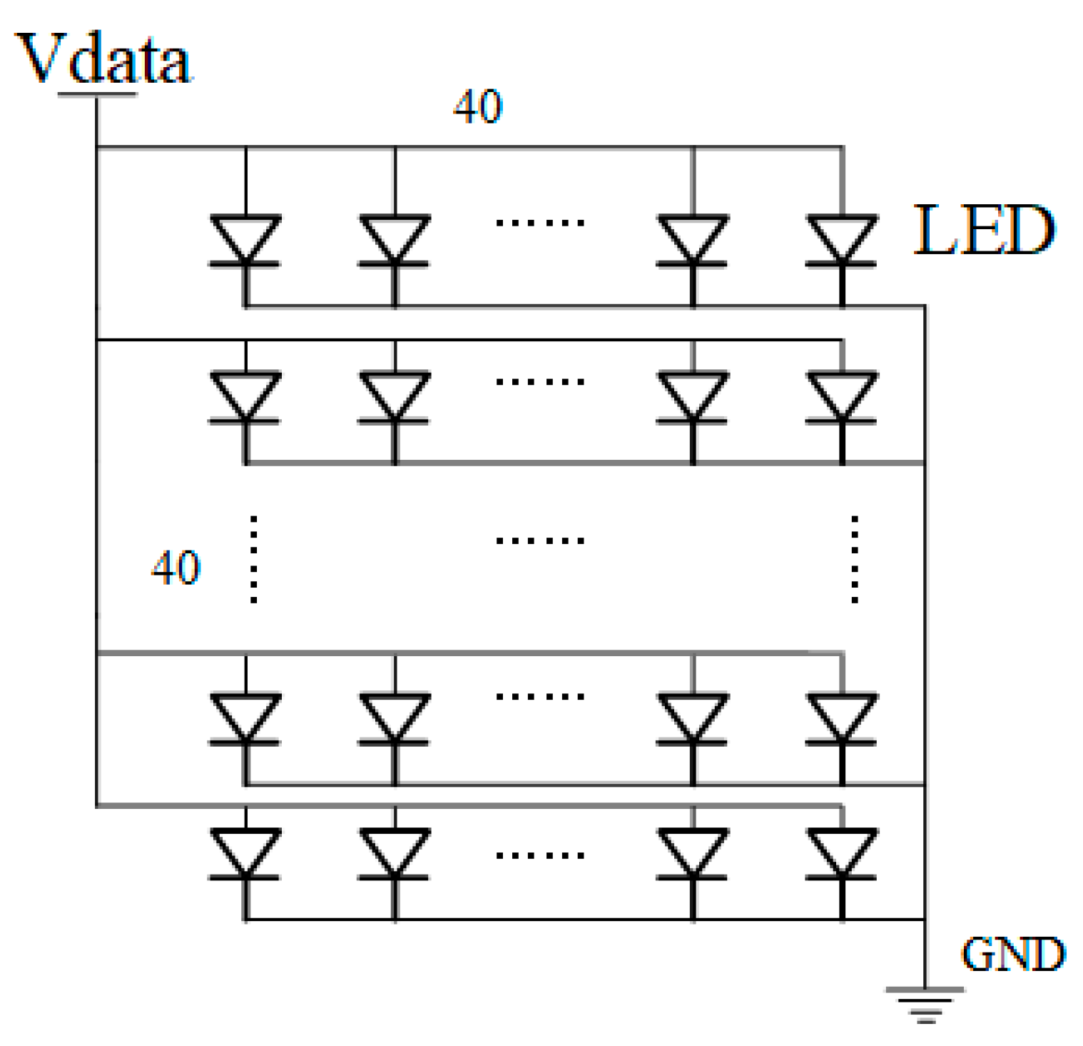
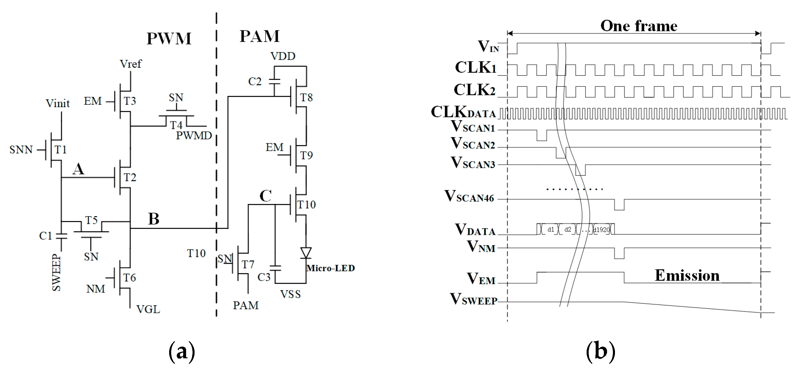
2.1. The Characteristics of Micro-LED

The production process of the blue and green micro-LED was as follows: Following the epitaxial growth process, the wafer was subjected to cleaning procedures, and inductively coupled plasma (ICP) dry etching was employed to etch the P-GaN layer and the active region of the multiple quantum well (MQW) until the N-GaN layer was exposed. Subsequently, indium tin oxide (ITO) was deposited on the P-type GaN layer as a transparent conductive layer. The epitaxial sheet was then rapidly thermally annealed in nitrogen in order to improve the ohmic contact between ITO and the GaN layer. A layer of chromium and gold was then deposited onto the sample in order to facilitate the formation of both the N and P contacts. The red micro-LED is different. Once the AlGaInP epitaxial wafer on the sapphire substrate has been obtained, the wafer is cleaned and then etched by ICP dry etching. The N-type AlGaInP layer and the active area of MQW are then passed through until the P-type AlGaInP layer is exposed. A layer of chromium and gold (Cr/Au) is deposited onto the sample in order to create a contact for the N and P contacts, respectively [15,16].
Then there is the design process for the 40 × 40 pixel array. Firstly, the PCB substrate is designed and prepared in accordance with the dimensions of the chip. Subsequently, the micro-LED chip is transferred to the PCB substrate by the method of solidification, thus completing the preparation of the array test module. The array is constructed with a 40 × 40 micro-LED connected in parallel within the array. This configuration ensures that the voltage source is driven directly outside, thus maintaining a consistent voltage load on each LED. The underlying principle is illustrated in Figure 1. Subsequently, the red, green, and blue LEDs are solidified on the substrate, resulting in the lamp board shown in Figure 2.
The configuration of the experimental apparatus is illustrated in Figure 3. The micro-LED array is positioned on the test bench of LED626. The power signal is directly loaded to the Vdata and GND on the carrier board. The brightness of the micro-LED is directly measured by LED626, and the resulting data are saved by the computer. In consideration of the prevailing experimental parameters, the solid crystal apparatus is capable of capturing LED chips with dimensions exceeding 152.4 μm × 88.9 μm. Consequently, the smallest feasible chip size was selected.
The target brightness and color temperature of the micro-LED display should be analogous to those of the mobile phone screen and car screen. Therefore, the maximum brightness of the target white field of the micro-LED was set at 1000 cd/cm², the minimum brightness at 0.010 cd/m², the color temperature at 9300 K, and the target brightness ratio of red, green, and blue at 3:6:1, as illustrated in Table 1.
Then the LED characteristics under the target brightness condition are measured. The complete experimental procedure is outlined below.
Step 1: The voltage source output mode should be set, commencing from 0 V and increasing by 0.01 V with each iteration, up to a maximum of 2.5 V. For each voltage increase, the brightness value should be recorded, along with the corresponding current value.
Step 2: In accordance with the first step, the maximum target brightness value and the corresponding voltage value of the red, green, and blue micro-LED arrays are extracted.
Step 3: In accordance with the methodology delineated in Step 1, the minimum target brightness value and the corresponding voltage value for the red, green, and blue micro-LED arrays are extracted.
Step 4: In accordance with the first step, the maximum target brightness value and the corresponding current value data for the red, green, and blue micro-LED arrays are extracted.
The results of the measurements of the three micro-LED arrays in red, green, and blue are presented in Table 2 and Table 3. The data indicate that when a voltage of 1.67 V is applied to the red micro-LED array, the brightness is 312 cd/m², whereas when a voltage of 1.36 V is applied, the brightness is 0.0030 cd/m². The application of a 2.08 V voltage to the green micro-LED array results in a brightness of 580 cd/m², whereas the application of a 1.79 V voltage to the same array yields a brightness of 0.0060 cd/m². The application of a voltage of 2.42 V to the blue micro-LED array results in a brightness of 97 cd/m², whereas the application of a voltage of 2.12 V to the same array results in a brightness of 0.0018 cd/m².
The data obtained in Step 4 indicate that the current required for a single red, green, and blue micro-LED chip to achieve the target maximum brightness of 1000 cd/m2 and color temperature of 9300 K are 8.7 μA, 1.8 μA, and 2.5 μA. This is shown in Table 4.
In order to achieve the uniformity of the whole screen of the micro-LED display, it is necessary to measure the brightness of each LED light-emitting chip in red, green, and blue, obtain the brightness difference of each chip, and then calculate the minimum grey level depth to eliminate the nonuniformity of the red, green, and blue chips. However, the brightness of each chip is not easily measured by the instrument, so a CCD camera is used to shoot the entire micro-LED array to extract the relative brightness value of each LED. The test process is shown in Figure 4.
The complete experimental procedure is outlined below.
Step 1: The output voltage source is 1.67 volts, and the red micro-LED array is illuminated.
Step 2: The CCD camera is used to capture the relative brightness of the red micro-LED array to the red light.
Step 3: In accordance with the values presented in Table 4, the voltage values of the green micro-LED array and the blue micro-LED array should be set to 2.08 V and 2.42 V, respectively, and Steps 1 and 2 should be repeated.

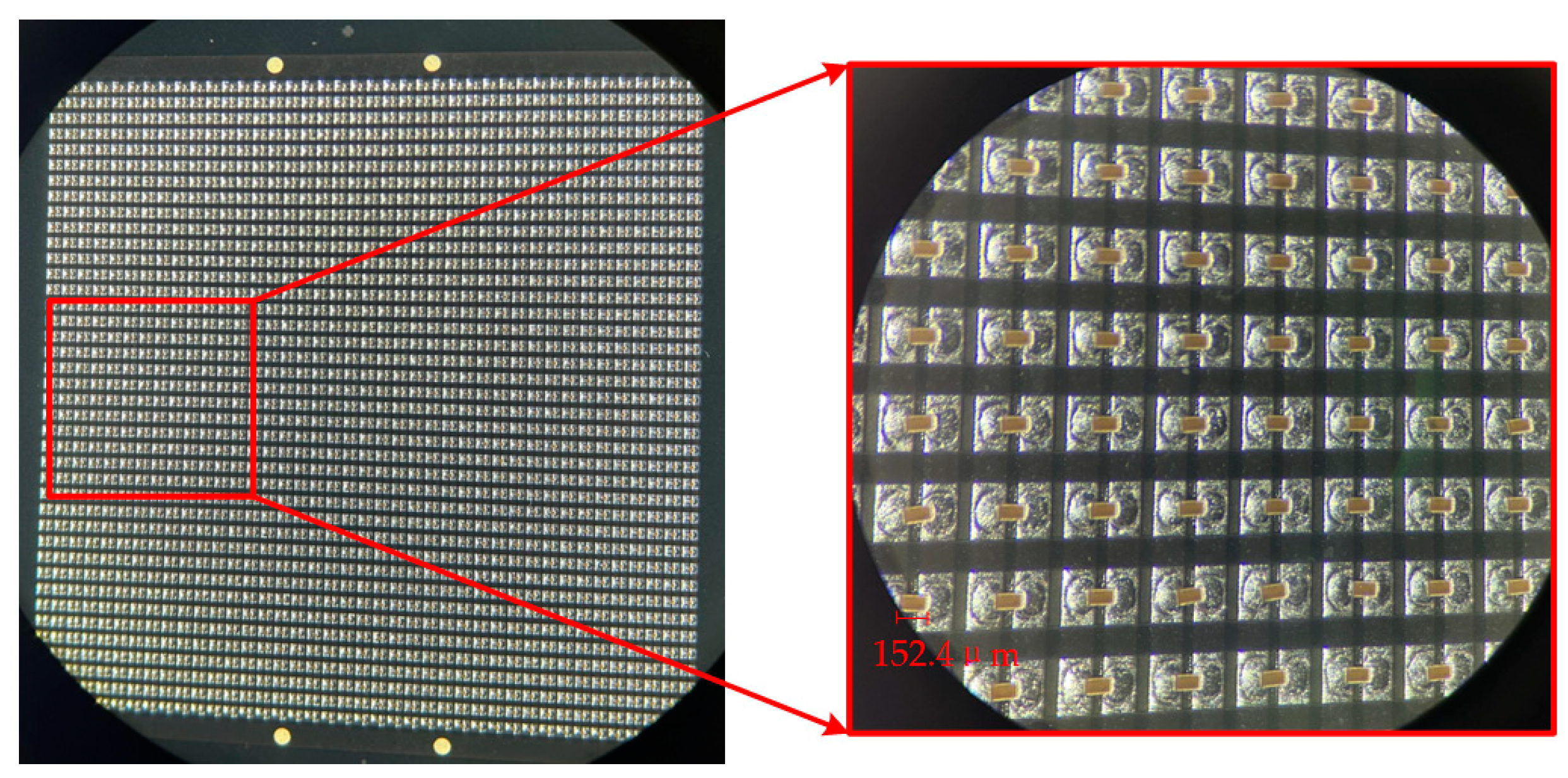
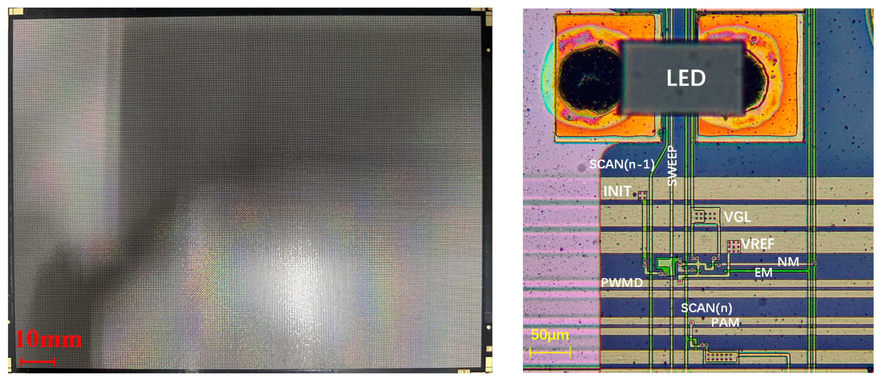
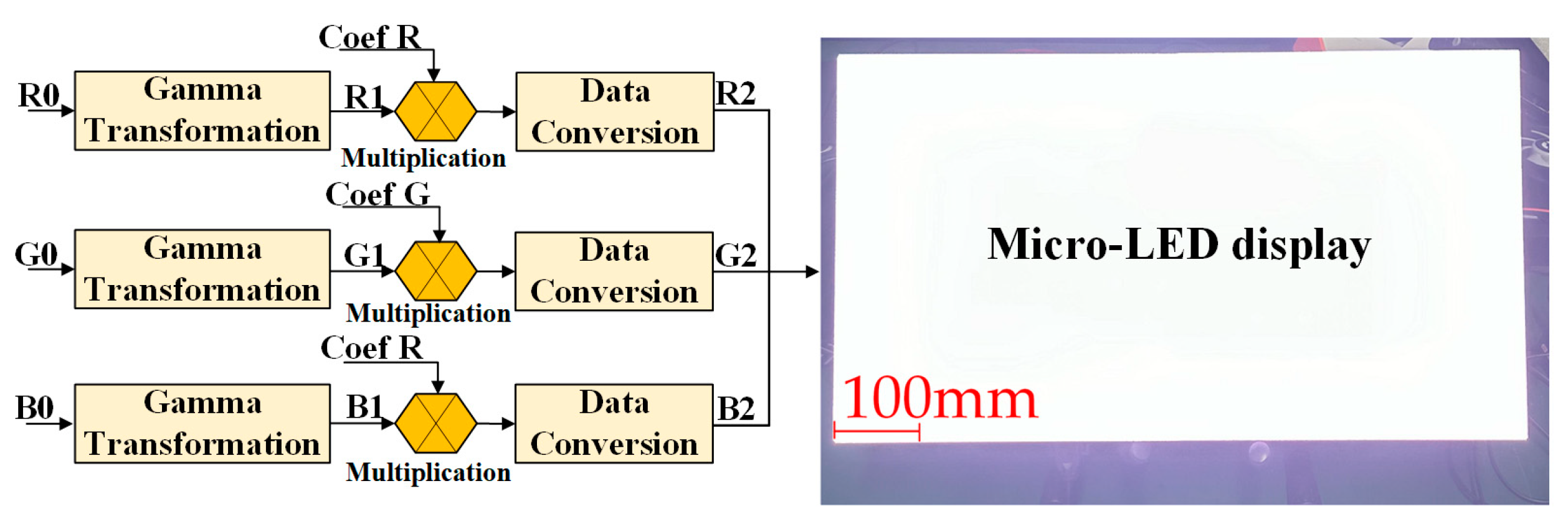
2.2. Preparation of Micro-LED Display Panel

The pixel circuit of the 10T3C is based on the LTPS design, and the schematic is shown in Figure 5a. The pixel circuit is composed of 10 TFTS and 3 capacitors. T1-T6 and C1 constitute the PWM part that controls the light-emitting time of the micro-LED display. T2 is used as a comparison tube to determine whether to release the gate charge of T8 by comparing the voltage relationship between the gate and the source of T2. T7-T10, C2, and C3 constitute the PAM part that controls the current amplitude. T10 is the driving TFT that controls the current amplitude, and the gate-source voltage is the controlling factor in this regard. In addition, the signals EM, NM, and SN are all control signals, while SWEEP is a harmonic signal used to generate a comparative luminous time. Figure 5b depicts a timing diagram. The circuit’s operational sequence is divided into three stages: reset, data writing, and luminescence [10].
(1) Reset: The SNN signal is reduced in amplitude, while the remaining signals are increased. The T1 tube is opened, and the Vinit signal is applied at point A. This results in a voltage of VA equal to that of Vinit.
(2) Data input and threshold voltage compensation: The SN signal is reduced, while the remaining signals are increased. The pulse-width modulation data (PWMD) signal is then compensated for by the threshold voltage of the T2 tube and input to point A. The VA value is then calculated as the sum of the PWMD and T1 voltages, which is equal to the PWMD voltage plus the T2 threshold voltage. Concurrently, the PAM data are introduced at point C.
(3) Comparative luminescence: The NM signal is pulled down, while the remainder of the signal remains at a high level. The T6 transistor is activated, with VB = VGL, and the T7 transistor is also activated. The EM signal is pulled down, and the T9 tube is opened, resulting in the illumination of the LED. VA = PWMD + VTH(T2) + SWEEP, with the reduction of the SWEEP signal, when VA < Vref + VTH(T2), the T4 transistor is activated, and the B point is set to VB = Vref. The T8 transistor tube is closed, and the LED ceases to emit light.
According to the TFT device current Formula (1), ILED, PWMD, VDD, and Vth10 are, respectively, the current flowing through the LED, the data voltage, the supply voltage, and the threshold voltage of T10. The μ, Cox, W, and L are, respectively, the carrier mobility, gate insulation capacitance per unit area, channel width, and channel length of T10 [10]. From the formula, it can be observed that the remaining values are fixed, with the exception of the value of W/L. In conjunction with the data presented in Table 5, W/L of T10 has been designed to be 70μ/7μ in order to meet the current output requirements when the maximum brightness of the white field is 1000 cd/m².
I L E D = 1 2 μ C o x W L P W M D V D D V t h 10 2
Figure 6 shows a photo of the LED fixed to the micro-LED panel by the mass-transfer technique after a single panel vane and a microscope image of a single sub-pixel.

3. Results

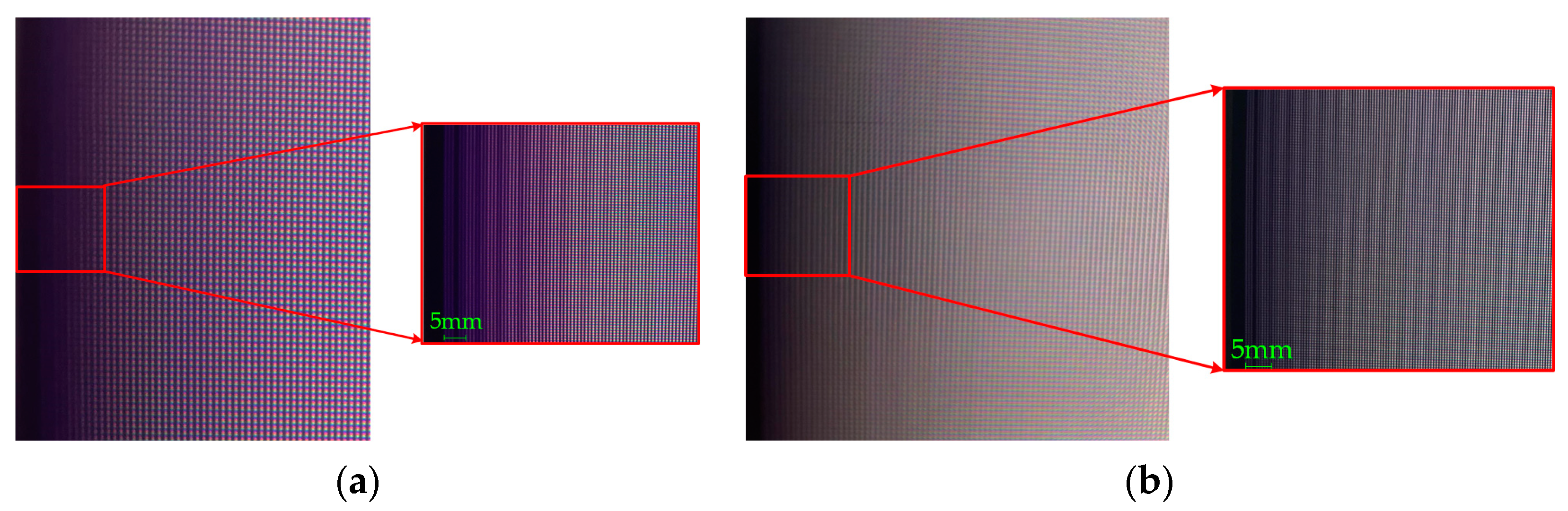
3.1. The Excessive Uniform Display in Greyscale

The I−V characteristics of the red, green, and blue chips can be obtained from the above experiments, as shown in Figure 7. The minimum and maximum operating voltages of the LED chips can be determined from the I–V curve. Additionally, the LED chip is a current-type device, exhibiting significant fluctuations in current within a relatively narrow data voltage range.
Assuming that the brightness of the white field changes linearly with the data voltage, the maximum brightness of the target white field corresponds to 255 grey level, and the minimum brightness corresponding to the target white field is 1 grey level. The data voltages of the red, green, and blue micro-LED arrays from 1 to 255 grey levels are 0.31 V, 0.29 V, and 0.30 V, respectively, under the condition that the target brightness of the white field is 1000 nits and the color temperature is 9300 K. The data voltage increment of each grey level can be calculated by determining the data voltage corresponding to the highest brightness and the data voltage corresponding to the lowest brightness. Upon incorporating the aforementioned data into the formula Δ V d a t a Δ g r a y , it can be determined that the voltage data for each grey level of the red, green, and blue micro-LED display arrays are 310 255 mV/grey, 290 255 mV/grey, and 300 255 mV/grey, as illustrated in Figure 8. It can be demonstrated that the minimum data voltage required to complete the red, green, and blue chip drives is the minimum common divisor of the three data values, which is 2 51 mV/grey. The greatest discrepancy in the data voltage of the red, green, and blue micro-LED display arrays is 0.31V for the red micro-LED display array. Consequently, the lowest greyscale can be calculated as follows: 0.31 V 2 51 m V / g r a y = 7905 . The figure of 7905 is greater than 4096 (12 bits) and less than 8192 (14 bits), thus indicating that the minimum grey level depth corresponding to the display driver control system is 13 bits.
In this way, we can use the 13-bit grey level depth control system to drive the red, green, and blue LED chips to accurately emit 0.0030 cd /m2, 0.0060 cd /m2, and 0.0018 cd /m2 brightness at a low grey level to complete the ratio of 3:6:1 and to achieve a 9300 K color temperature white field display. Concurrently, the brightness of 312 cd/m², 580 cd/m², and 97 cd /m² can be precisely emitted during periods of high brightness, thereby achieving a ratio of 3:6:1 and a color temperature of 9300 K for the display. This enables the micro-LED display to achieve a uniform display with no color bias from a low grey level of 0.01 cd/m2 to a high brightness level of 1000 cd/m2.
Considering the difference in visual perception of human eyes, it can be seen that when the color difference value of the micro-LED display is less than 0.5, human eyes cannot recognize the difference between two colors. The corresponding grey depth requirements for the uniform display of red, green, and blue micro-LEDs are shown in Table 5 [17]. As shown in the table, when the control system has a 12-bit greyscale display, the human eye cannot detect the difference in color.
As illustrated in Figure 9, the use of the micro-LED display based on LTPS with an 8-bit greyscale depth control is associated with the generation of excessive grey levels that lack smoothness and exhibit color bias issues. Conversely, the deployment of 12-bit greyscale depth control can facilitate the attainment of a brightness ratio of 3:6:1 for each grey level, thereby addressing the challenges of brightness and color deviation that may arise from the employment of an unorthodox ratio for certain grey levels.

3.2. Uniform Brightness Display

The high pixel-density of micro-LEDs makes it challenging to accurately measure the absolute brightness of each LED, which is necessary to study their characteristic differences. Consequently, the relative brightness values of all chips in the three micro-LED arrays (red, green, and blue) can be obtained by shooting with the CCD camera, after which a graph can be drawn with MATLAB [18], as illustrated in Figure 10. The data indicate a significant disparity in brightness levels between the red, green, and blue chips. The maximum brightness relative value of the red micro-LED array chip is 1,378,624, the minimum brightness relative value is 883,872, and the average relative brightness value is 1,117,742. The maximum relative brightness value of the green micro-LED array chip is 1,075,280, the minimum relative brightness value is 695,488, and the average relative brightness value is 893,925. The maximum relative brightness value of the blue micro-LED array chip is 1,248,064, the minimum relative brightness value is 517,488, and the average relative brightness value is 835,521. The brightness range of the red micro-LED array is 64.8–101.2%, the brightness range of the green micro-LED array is 66.5–102.8%, and the brightness range of the blue micro-LED array is 53.5–129.2%.
Formula (2) indicates that the LED correction factor is typically calculated as the ratio of the mean relative brightness of the entire screen to the relative brightness of a single LED, where Ci represents the correction factor, Si represents the mean relative brightness of the entire screen, and G represents the relative brightness of a single LED. The data presented above allow us to calculate that the correction factor of the maximum relative brightness LED of the red micro-LED array is 0.64861, while the correction factor of the minimum relative brightness LED is 1.01167. Consequently, the minimum common divisor of the two is 0.00001. It is therefore evident that a minimum grey level depth of 14 bits is required for the red micro-LED array to display in a uniform manner following the aforementioned corrections. For the green micro-LED array, the correction factor of the maximum relative brightness LED is 0.66507, and the correction factor of the minimum relative brightness LED is 1.02826. Furthermore, the minimum common divisor of the two is 0.00001. Consequently, at least 14 bits of grey level depth are required to display the green micro-LED array uniformly through correction. For the blue micro-LED array, the correction factor of the maximum relative brightness LED is 0.53556, and the correction factor of the minimum relative brightness LED is 1.29166. Furthermore, the minimum common divisor of the two is 0.00002. Consequently, at least 13 bits of grey level depth are required to display the green micro-LED array uniformly through correction.
C i = 0.8 G S i
As indicated in Table 6, in order to achieve a uniform brightness display under a white field target brightness of 1000 cd/m2 and 9300 K color temperature conditions, a grey level depth of 12-bit is required.
We seamlessly spliced the LTPS-based micro-LED display module into a large screen, and then the micro-LED display based on LTPS was collected by CCD, and the correction data corresponding to red, green, and blue were calculated. The 12-bit control system was used to load the correction data into the display data; the calibration process is illustrated in Figure 11 [19]. The corrected relative brightness values of red, green, and blue were then collected by CCD.
The International Commission on Display Measurement recommends brightness uniformity as a measure of the degree to which the brightness of the screen surface is uniform, and the specific method is to randomly select nine display arrays across the full screen area and display a particular primary color across the full screen at the highest grey level and brightness [20]. After conducting brightness correction, the nine-point method is used to measure the brightness values of the RGB at maximum brightness. The value is shown in Table 6. The brightness uniformity of RGB can be calculated using Equation (3).
L J = 1 L i L m e a n L m e a n × 100 %
L ¯ = i = 1 N L i
You can see that using the grey level depth of a 12-bit control system to debug a micro-LED display can achieve a brightness uniformity of 84.1–97.1%. Table 6 and Table 7 show the brightness data of red, green, and blue primary colors before and after compensation, respectively.

4. Conclusions

In summary, we proposed a study of the photoelectric characteristics of a red–green–blue light-emitting chip with a size of 152.4 μm × 88.9 μm. It is found that the data voltage of the red–green–blue chip is inconsistent under the condition that the target brightness of the white field is 1000 nits and the color temperature is 9300 K. In order to achieve the uniform display of the white field, a control system with a depth of 12-bit greyscale is needed. A 10T3C pixel driver circuit based on LTPS was designed, and a chip of 152.4 μm × 88.9 μm was bonded to the substrate to produce a micro-LED display. The 12-bit greyscale is achieved through the implementation of an external drive control mechanism. After brightness correction, the uniformity of the micro-LED display reaches 84.4–97.1%.

Author Contributions

Conceptualization, X.Z. and X.M.; methodology, H.C. and Y.C. (Yu Chen); software, Z.X. and F.L.; validation, J.C.; formal analysis, Y.W. and D.H.; writing—review and editing, Y.C. (Yufeng Chen). All authors have read and agreed to the published version of the manuscript.

Funding

This research was funded in part by the major science and technology special projects of Jilin Province, grant number 20210301001GX and grant 20210301002GX; in part by Jilin Province science and technology development plan, project grant number 20230204098YY; in part by Jilin Province science and technology development plan, project grant number 20230201001GX; and in part by Jilin Province science and technology development plan, project grant number 20240301001GX.

Data Availability Statement

Data are contained within the article.

Conflicts of Interest

Author Xinyue Mao and Zicheng Xu was employed by the company Changchun Cedar Electronics Technology Co., Ltd. The remaining authors declare that the research was conducted in the absence of any commercial or financial relationships that could be construed as a potential conflict of interest.

References

  1. Chen, Z.; Yan, S.; Danesh, C. MicroLED technologies and applications: Characteristics, fabrication, progress, and challenges. J. Phys. D Appl. Phys. 2021, 54, 123001. [Google Scholar] [CrossRef]
  2. Huang, Y.; Hsiang, E.-L.; Deng, M.-Y.; Wu, S.-T. Mini-LED, Micro-LED and OLED display: Present status and future perspectives. Light Sci. Appl. 2020, 9, 105. [Google Scholar] [CrossRef] [PubMed]
  3. Lin, J.Y.; Jiang, H.X. Development of Micro-LED. Appl. Phys. Lett. 2020, 116, 100502. [Google Scholar] [CrossRef]
  4. Wu, T.; Sher, C.-W.; Lin, Y.; Lee, C.-F.; Liang, S.; Lu, Y.; Chen, S.-W.H.; Guo, W.; Kuo, H.-C.; Chen, Z. Mini-LED and micro-LED: Promising candidates for the next generation display technology. Appl. Sci. 2018, 8, 1557. [Google Scholar] [CrossRef]
  5. Chang, K.-P.; Lien, P.-C.; Yen, C.-C.; Chen, P.-W.; Horng, R.-H.; Wuu, D.-S. High performance AlGaInP-based micro-LED display with novel pixel structures. IEEE Photon. Technol. Lett. 2021, 33, 1375–1378. [Google Scholar] [CrossRef]
  6. Chen, G.; Craven, M.; Kim, A.; Munkholm, A.; Watanabe, S.; Camras, M.; Götz, W.; Steranka, F. Performance of high-power III-nitride light emitting diodes. Phys. Status Solidi A 2008, 205, 1086–1092. [Google Scholar] [CrossRef]
  7. Kim, J.-H.; Shin, S.; Kang, K.; Jung, C.; Jung, Y.; Shigeta, T.; Park, S.-Y.; Lee, H.S.; Min, J.; Oh, J.; et al. 15-1: PWM Pixel Circuit with LTPS TFTs for Micro-LED Display. SID Symp. Dig. Tech. Pap. 2019, 50, 192–195. [Google Scholar] [CrossRef]
  8. Oh, J.; Kim, J.-H.; Lee, J.; Jung, E.K.; Oh, D.; Min, J.; Im, H.; Kim, Y.-S. Pixel Circuit with P-Type Low-Temperature Polycrystalline Silicon Thin-Film Transistor for Micro Light-Emitting Diode Display Using Pulse width Modulation. IEEE Electron Device Lett. 2021, 42, 1496–1499. [Google Scholar] [CrossRef]
  9. Zou, P.-A.; Xu, Y.-G.; Liu, C.; Zhang, L.-R.; Zhang, J.-H.; Yuan, Y.-K.; Cai, W.; Han, S.-H.; Zhou, L.; Xu, M.; et al. A New Analog PWM Pixel Circuit with Metal Oxide TFTs for Micro-LED display. IEEE Trans. Electron Devices 2022, 69, 4306–4311. [Google Scholar] [CrossRef]
  10. Li, S.; Wu, W.; Chen, C.; Chuai, X.; Zhang, C.; Gu, C.; Liu, Y.; Lu, N.; Geng, D.; Li, L. Novel A-IGZO TFT Pixel Driving Circuit Using Hybrid PWM and PAM Method With Lower Power Consumption for Micro-LED Display. IEEE Electron Device Lett. 2024, 45, 1024–1027. [Google Scholar] [CrossRef]
  11. Xiao, J.; Huo, W.; Yuan, D.; Liang, C.; Lai, G.; Li, J.; Xu, H.; Li, S.; Zhang, S. A New Pixel Circuit for Micro-Light Emitting Diode Display With Pulse Hybrid Modulation Driving and Compensation. IEEE J. Electron Devices Soc. 2023, 12, 1–6. [Google Scholar] [CrossRef]
  12. Lin, Y.-Z.; Liu, C.; Zhang, J.-H.; Yuan, Y.-K.; Cai, W.; Zhou, L.; Xu, M.; Wang, L.; Wu, W.-J.; Peng, J.-B. Active-Matrix Micro-LED display Driven by Metal Oxide TFTs Using Digital PWM Method. IEEE Trans. Electron Devices 2021, 68, 5656–5661. [Google Scholar] [CrossRef]
  13. Sohn, Y.; Moon, G.; Choi, K.; Kim, Y.; Park, K. Effects of TFT Mobility Variation in the Threshold Voltage Compensation Circuit of the OLED Display. J. Inf. Disp. 2016, 18, 25–30. [Google Scholar] [CrossRef]
  14. Hong, Y.-H.; Jung, E.K.; Hong, S.; Kim, Y.-S. 61-2: A Novel Micro-LED Pixel Circuit Using N-type LTPS TFT with Pulse Width Modulation Driving. SID Symp. Dig. Tech. Pap. 2021, 52, 868–871. [Google Scholar] [CrossRef]
  15. Li, Y.; Tao, J.; Zhao, Y.; Wang, J.; Lv, J.; Qin, Y.; Liang, J.; Wang, W. 48 × 48 pixelated addressable full-color micro display based on flip-chip micro LEDs. Appl. Opt. 2019, 58, 8383–8389. [Google Scholar] [CrossRef] [PubMed]
  16. Li, Y.; Tao, J.; Wang, Q.; Zhao, Y.; Sun, Y.; Li, P.; Lv, J.; Qin, Y.; Wang, W.; Zeng, Q.; et al. Microfluidics-based quantum dot color conversion layers for full-color micro-LED display. Appl. Phys. Lett. 2021, 118, 173501. [Google Scholar] [CrossRef]
  17. Zhao, X.; Wang, R.; Zheng, X.; Hao, Y.; Chen, Y. Systemic Accuracy Analysis of LED Display Based on Visual Perception. Chin. J. Liq. Cryst. Disp. 2012, 27, 324–331. [Google Scholar] [CrossRef]
  18. Huang, S.; Zheng, X.; Mao, X.; Chen, Y.; Chen, Y. Vignetting Compensation Method for CMOS Camera Based on LED Spatial Array. Electronics 2024, 13, 1936. [Google Scholar] [CrossRef]
  19. Chen, Y.; Zheng, X.; Cao, H.; Wang, Y.; Cheng, H.; Chen, J.; Huang, S.; Li, J.; Huang, D.; Chen, Y. High Precision Control System for Micro-LED Display. Appl. Sci. 2023, 13, 10601. [Google Scholar] [CrossRef]
  20. ICDM Display Metrology Standard. Available online: https://www.icdm-sid.org/ (accessed on 22 April 2024).
Figure 1. The connection diagram for the red, green, and blue test arrays.
Electronics 13 03369 g001
Figure 2. The red, green, and blue LEDs are solidified on the substrate.
Electronics 13 03369 g002
Figure 3. The flow chart of the experiment.
Electronics 13 03369 g003
Figure 4. Relative brightness measurement.
Electronics 13 03369 g004
Figure 5. The 10T3C pixel circuit schematic (a) and the timing diagram (b).
Electronics 13 03369 g005
Figure 6. The micro-LED panel after LED mass-transferring and micrograph of the fabricated 10T3C pixel circuit.
Electronics 13 03369 g006
Figure 7. I–V characteristic of red, green, and blue LED.
Electronics 13 03369 g007
Figure 8. Vdata range, Δ V d a t a /grey of red, green, and blue LEDs.
Electronics 13 03369 g008
Figure 9. The images exhibit an uneven greyscale (a) and an even greyscale (b).
Electronics 13 03369 g009
Figure 10. The grey truth value before correction of red (a), green (b), and blue (c).
Electronics 13 03369 g010aElectronics 13 03369 g010b
Figure 11. Brightness correction.
Electronics 13 03369 g011
Table 1. Maximum and minimum target luminance values of white, red, green, and blue.
Maximum Target Luminance (cd/m2)Minimum Target Luminance (cd/m2)
White10000.010
Red3000.003
Green6000.006
Blue1000.001
Table 2. The actual measured value and the target value of white, red, green, and blue.
Luminance of Sample (cd/m2)Target Luminance (cd/m2)
MaxMinMaxMin
Red3120.00303000.003
Green5800.00606000.006
Blue970.00181000.001
Table 3. The actual measured Vdata for maximum luminance and minimum luminance.
Applied Vdata for
Maximum Luminance (V)
Applied Vdata for
Minimum Luminance (V)
Red1.671.36
Green2.081.79
Blue2.422.12
Table 4. The current values at the maximum brightness of white, red, green, and blue.
Maximum Luminance (cd/m2)Panel Current (mA)Single LED Current (μA)
Red312148.7
Green58031.8
Blue9742.5
Table 5. The grey level depth for the micro-LED display.
RedGreenBlue
Grey depth (bits)111210
Table 6. White luminance of LED cabinet before vignetting compensation (cd/m2).
Position123456789 L J W
160170063064163554656557155384.2%
260358358654656854258657067384.7%
359768260356356454559956959784.6%
459660168955361253558956861384.2%
L ¯ 84.4%
Table 7. White luminance of LED cabinet after vignetting compensation (cd/m2).
Position123456789 L J W
158160060159858358957557158397.3%
258059960059758358957157058297.3%
358159859859758358957456958297.1%
458059759959758158757456858297.0%
L ¯ 97.1%
Disclaimer/Publisher’s Note: The statements, opinions and data contained in all publications are solely those of the individual author(s) and contributor(s) and not of MDPI and/or the editor(s). MDPI and/or the editor(s) disclaim responsibility for any injury to people or property resulting from any ideas, methods, instructions or products referred to in the content.

