
High-Speed Signal Optimization at Differential VIAs in Multilayer Printed Circuit Boards

 , , , , and
Abstract
:1. Introduction
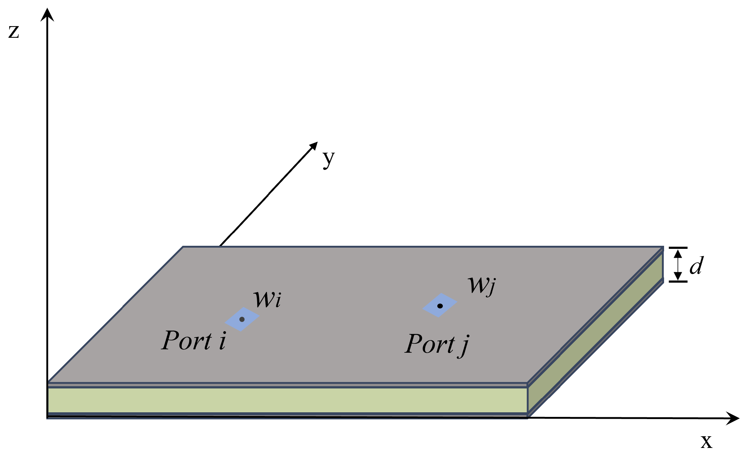
2. Theoretical Analysis of Resonance
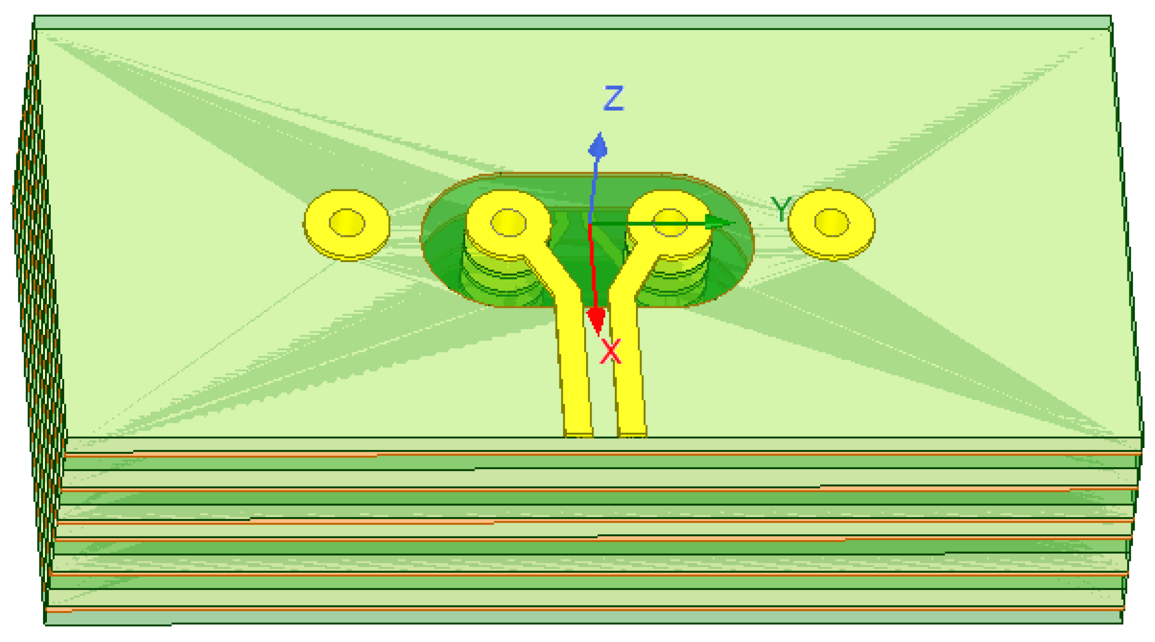
3. VIA Modeling
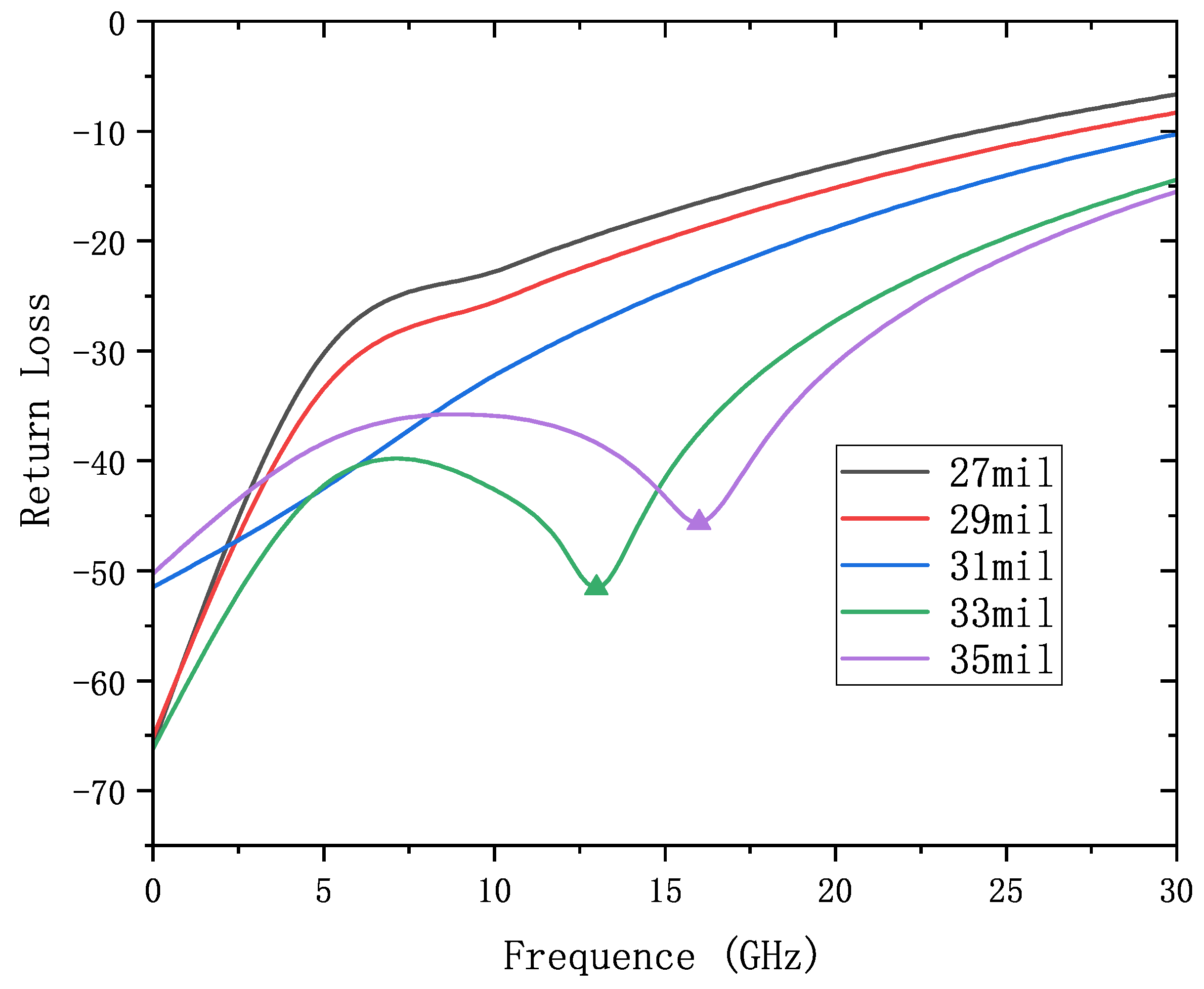
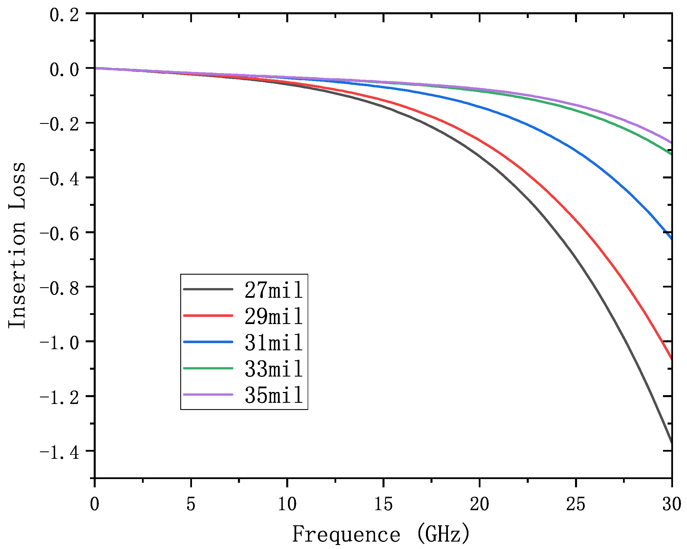
3.1. Parametric Analysis of VIA Stub Length
3.2. Parametric Analysis of Anti-Pad Radius
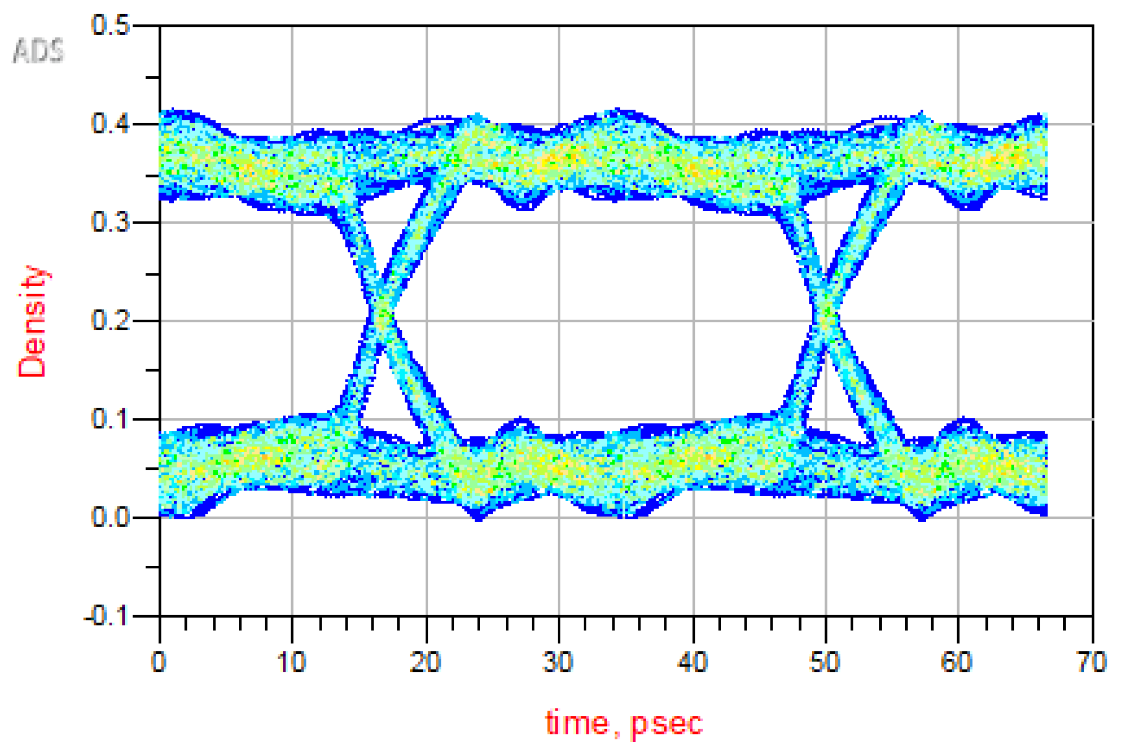
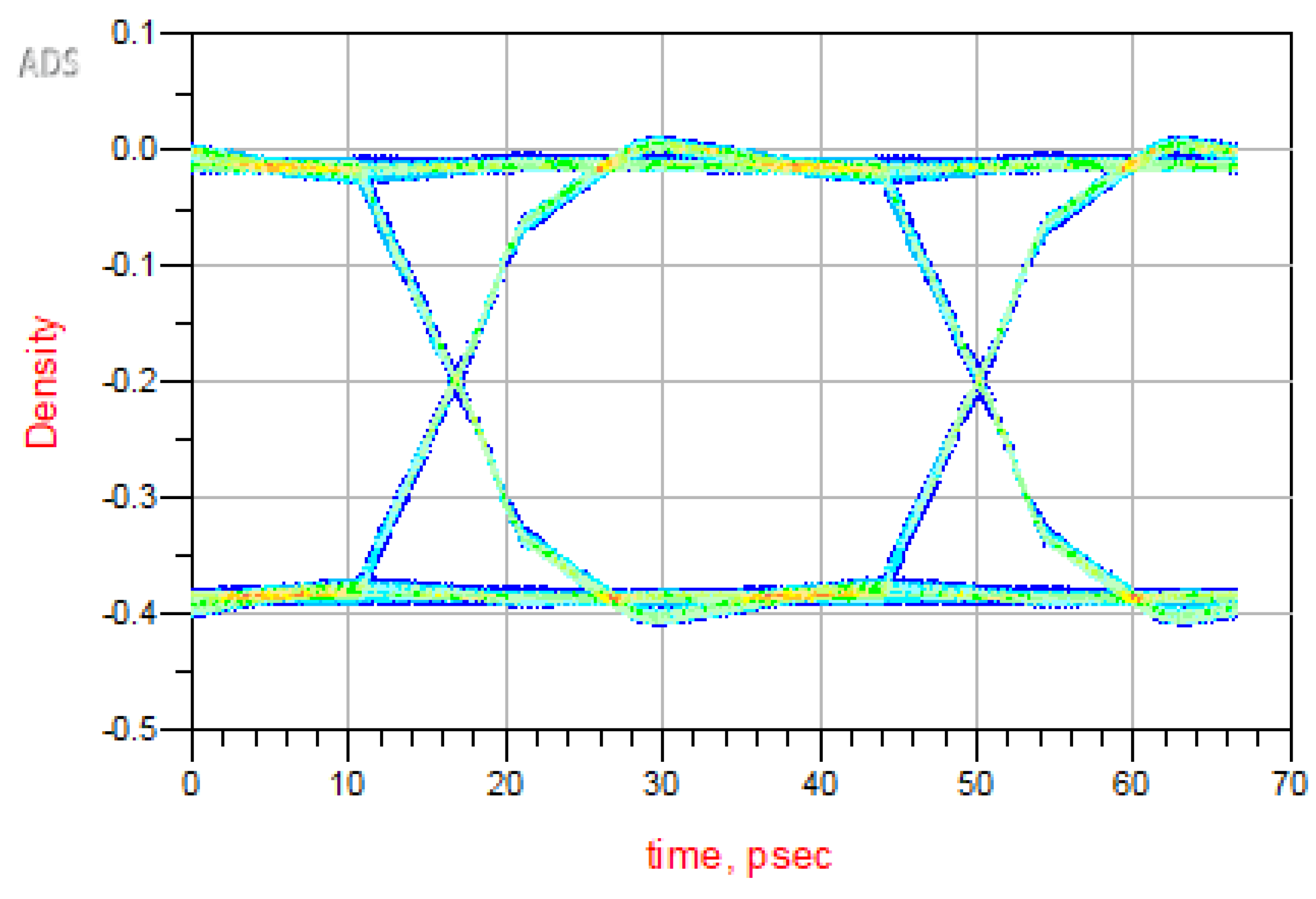
3.3. Optimization and Verification
4. Conclusions
Author Contributions
Funding
Data Availability Statement
Conflicts of Interest
References
- Kim, J.; Pak, J.S.; Cho, J.; Song, E.; Cho, J.; Kim, H.; Song, T.; Lee, J.; Lee, H.; Park, K.; et al. High-Frequency Scalable Electrical Model and Analysis of a Through Silicon Via (TSV). IEEE Trans. Compon. Packag. Manuf. 2011, 1, 181–195. [Google Scholar] [CrossRef]
- Steenbergen, E.; Moonen, N.; Leferink, F. 3D Full-Wave Simulation of Stub Length Effect of Vias in High Speed PCB Design. In Proceedings of the 2021 Asia-Pacific International Symposium on Electromagnetic Compatibility (APEMC), Nusa Dua, Indonesia, 27–30 September 2021; pp. 1–4. [Google Scholar] [CrossRef]
- Shi, H.; Siow, C.T.; Yohan, F.; Hongtao, Z.; Jack, C.; Sai, L.C.; David, M. Advanced Packaging Technology and Die-Package-PCB Co-Design for 56G NRZ FPGA. In Proceedings of the DesignCon, Santa Clara, CA, USA, 31 January–1 February 2018. [Google Scholar]
- Hu, K. Design and characterization of differential Signal Integrity interconnects at Millimeter-Wave PCB. In Proceedings of the 2020 IEEE International Symposium on Electromagnetic Compatibility and Signal/Power Integrity (EMCSI), Reno, NV, USA, 28 July–28 August 2020; pp. 90–95. [Google Scholar] [CrossRef]
- Prasun, P.; Kamal, S.; Bartoszewicz, A.; Ghosh, S. Difference Equation With Minima-Based Discrete-Time Sliding Mode Control. IEEE Trans. Circuits Syst. II Express Briefs 2023, 70, 4404–4408. [Google Scholar] [CrossRef]
- Sheng, H.; Feng, Q. A Broadband Stepped Configuration of Substrate Integrated Waveguide Vertical Transition Structure. IEEE Trans. Circuits Syst. II Express Briefs 2024, 71, 1799–1803. [Google Scholar] [CrossRef]
- Steinberger, M.; Telian, D.; Michael, T.; Vishwanath, I.; Janakinadh, Y. Proper Ground Return Via Placement for 40+ Gbps Signaling. In End-to-End High-Speed Digital Design; Signal Integrity Journal: Norwood, MA, USA, 2023; p. 37. [Google Scholar]
- Richard, L.; Suomin, C.; Simian, S.; Jian, L. Optimal Design and Swift Workflow for Multi-layer Structures. In Proceedings of the Design Con, Santa Clara, CA, USA, 31 January–2 February 2023. [Google Scholar]
- Michael, S.; Donald, T.; Orlando, B.; Kevin, R. Managing Differential via Crosstalk and Ground via Placement for 40+ Gbps Signaling. In Proceedings of the Design Con, Santa Clara, CA, USA, 31 January–2 February 2023. [Google Scholar]
- Li, C.; Cai, K.; Mathew, M.K.; Mousavi, S.; Ouyang, M.; Sen, B.; Kim, D.B. High-Speed Differential Via Optimization using a High-Accuracy and High-Bandwidth Via Model. In Proceedings of the 2023 IEEE Symposium on Electromagnetic Compatibility and Signal/Power Integrity (EMC+SIPI), Grand Rapids, MI, USA, 29 July–4 August 2023; pp. 280–285. [Google Scholar] [CrossRef]
- Deng, Y.; Li, Z.; Yu, Y.; Li, B.; Wang, X.; Wu, Z. S Parameters Optimization of High-Speed Differential Vias Model on A Multilayer PCB. In Proceedings of the 2022 23rd International Conference on Electronic Packaging Technology (ICEPT), Dalian, China, 10–13 August 2022; pp. 1–4. [Google Scholar] [CrossRef]
- Li, K.; Li, Y.; Han, X.; Ding, D.; He, W.; Su, Z.; Shi, S. Experiment and Simulation Studies on Resonances due to Period Structure in PCBs. In Proceedings of the DesignCon 2022, Santa Clara, CA, USA, 5–7 April 2022. [Google Scholar]
- Bogatin, E.; Li, Y.; Liu, Y.; Chu, X.; Lu, J. Signal Integrity and Power Integrity Analysis; Publishing House of Electronics Industry: Beijing, China, 2019; pp. 79–125. [Google Scholar]
- Zhang, Y.; Xu, J.; Zhang, A. Generative Model for Dual-Band Filters Based on Modified Complementary Split-Ring Resonators. Electronics 2024, 13, 2321. [Google Scholar] [CrossRef]
- Tian, X.; Zhang, Y.J. Analysis of via resonance in multi-layer printed circuit board. In Proceedings of the 2018 International Workshop on Antenna Technology (iWAT), Nanjing, China, 5–7 March 2018; pp. 1–3. [Google Scholar] [CrossRef]
- Ge, J.; Floyd, R.; Khan, A.; Wang, G. High-Performance Interconnects With Reduced Far-End Crosstalk for High-Speed ICs and Communication Systems. IEEE Trans. Compon. Packag. Manuf. 2023, 13, 1013–1020. [Google Scholar] [CrossRef]
- Xie, T.; Wang, X.; Zhu, L.; Lu, G. A Synthesis Theory of Stripline Dual-Band Filtering Power Divider With Controllable Full-Frequency Isolation. IEEE Trans. Compon. Packag. Manuf. 2024, 14, 693–704. [Google Scholar] [CrossRef]
- Cao, W.; Chen, X. On the Influence of Fractional-Order Resonant Capacitors on Zero-Voltage-Switching Quasi-Resonant Converters. Electronics 2024, 13, 2562. [Google Scholar] [CrossRef]
- Li, W.; Zhang, J.; Gao, L.; Chen, H.; Wang, L.; Fang, Z.; Cai, X.; Li, Y. Compact TGV-Based Bandpass Filters Using Integrated Dual Composite Right/Left-Handed Resonators. IEEE Trans. Circuits Syst. II Express Briefs 2024, 71, 1939–1943. [Google Scholar] [CrossRef]
- Zheng, Y.; Wang, W.; Wu, Y. Planar Coupled-Line-Based Flat Negative Group Delay Microwave Circuit With Size Reduced and Bandwidth Enhanced. IEEE Trans. Circuits Syst. II Express Briefs 2023, 70, 4339–4343. [Google Scholar] [CrossRef]
- Regev, D.; Zolkov, E.; Cohen, E. S-Parameter Analysis and Compact Formulation of Two-Port 90° N-Path Circuits. IEEE Trans. Circuits Syst. II Express Briefs 2022, 69, 4679–4683. [Google Scholar] [CrossRef]
- Rodríguez-Velásquez, Y.; Torres-Torres, R.; Murphy-Arteaga, R. Identifying and Modeling Resonance-Related Fluctuations on the Experimental Characteristic Impedance for PCB and On-Chip Transmission Lines. Electronics 2023, 12, 2994. [Google Scholar] [CrossRef]
- Juarez, D.M.; Mathieu, F.; Libaude, G.; Bourrier, D.; Charlot, S.; Mazenq, L.; Conédéra, V.; Salvagnac, L.; Dufour, I.; Nicu, L. A Simple Process for the Fabrication of Parallel-Plate Electrostatic MEMS Resonators by Gold Thermocompression Bonding. In Proceedings of the 2023 IEEE 36th International Conference on Micro Electro Mechanical Systems (MEMS), Munich, Germany, 15–19 January 2023; pp. 643–646. [Google Scholar] [CrossRef]
- Reljic, B.M.; Simic, S.M.; Golubicic, Z.T.; Zejak, A.J. Novel mmWave low-loss narrow-bandwidth highly selective filter with PCB integrated dielectric resonators for demanding ground and space applications. In Proceedings of the 2023 31st Telecommunications Forum (TELFOR), Belgrade, Serbia, 21–22 November 2023; pp. 1–3. [Google Scholar] [CrossRef]
- Zhou, P.; Sang, S.; Huang, Q.; Ma, C. Impact of Anti-resonance Caused by Via Structure on Signal Integrity in High-Speed Circuits. In Proceedings of the 2019 IEEE 3rd Advanced Information Management, Communicates, Electronic and Automation Control Conference (IMCEC), Chongqing, China, 11–13 October 2019; pp. 867–871. [Google Scholar] [CrossRef]
- Avitabile, G.; Florio, A.; Gallo, V.L.; Pali, A.; Forni, L. An Optimization Framework for the Design of High-Speed PCB VIAs. Electronics 2022, 11, 475. [Google Scholar] [CrossRef]
- Biswaranjan, B.; Kalirasu, A. Design and Performance Analysis of Through Hole Via. In Proceedings of the 2021 2nd International Conference for Emerging Technology (INCET), Belagavi, India, 21–23 May 2021; pp. 1–5. [Google Scholar] [CrossRef]
- Shiue, G.H.; Yeh, C.L.; Liu, L.S.; Wei, H.; Ku, W.C. Influence and Mitigation of Longest Differential via Stubs on Transmission Waveform and Eye Diagram in a Thick Multilayered PCB. IEEE Trans. Compon. Packag. Manuf. 2014, 4, 1657–1670. [Google Scholar] [CrossRef]
- Gu, Z.; Zhang, L.; Jin, H.; Tao, T.; Li, D.; Li, E.P. Deep Reinforcement Learning-Based Ground-Via Placement Optimization for EMI Mitigation. IEEE Trans. Electromagn. Compat. 2023, 65, 564–573. [Google Scholar] [CrossRef]
- Yeh, C.L.; Tsai, Y.C.; Hsu, C.M.; Liu, L.S.; Tsai, S.H.; Kao, Y.H.; Shiue, G.H. Influence of via stubs with different terminations on time-domain transmission waveform and eye diagram in multilayer PCBs. In Proceedings of the 2012 IEEE Electrical Design of Advanced Packaging and Systems Symposium (EDAPS), Taipei, Taiwan, 9–11 December 2012; pp. 149–152. [Google Scholar] [CrossRef]
- Korobkov, M.A.; Vasilyev, F.V.; Khomutskaya, O.V. Analytical Model for Evaluating the Reliability of Vias and Plated Through-Hole Pads on PCBs. Inventions 2023, 8, 77. [Google Scholar] [CrossRef]
- Shen, Y.; Wang, H.; Blaabjerg, F.; Zhao, H.; Long, T. Thermal Modeling and Design Optimization of PCB Vias and Pads. IEEE Trans. Power Electron. 2020, 35, 882–900. [Google Scholar] [CrossRef]
- Peng, Z.; Xu, H.; Su, D. A Method of Extracting Transmission Characteristics of Interconnects from Near-Field Emissions in PCBs. Appl. Sci. 2023, 13, 2874. [Google Scholar] [CrossRef]
- Li, W.; Liu, Z.; Qian, W.; Wang, Z.; Wang, W.; Zhao, Y.; Zhang, X. Modeling of the RF Coaxial TSV Configuration Inside the Silicon Interposer With Embedded Cooling Cavity. IEEE Trans. Compon. Packag. Manuf. 2022, 12, 3–10. [Google Scholar] [CrossRef]


| Optimization Scheme | Measures Taken |
|---|---|
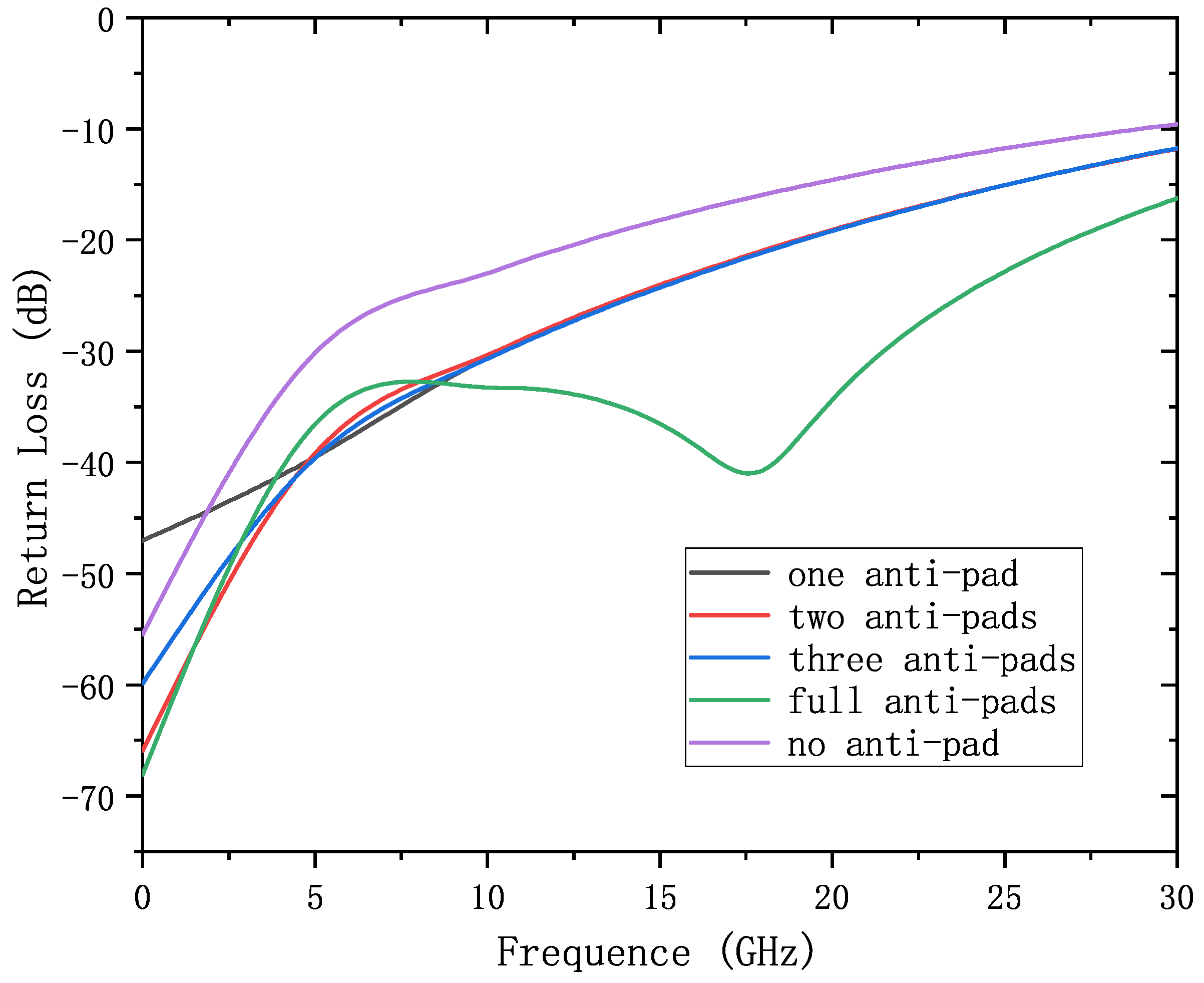
| Scheme 1 | The influence of the back-drill length on the S-parameter was investigated by keeping the VIA radius and anti-pad radius constant. |
| Scheme 2 | The influence of the anti-pad radius on the S-parameter was investigated by keeping the VIA radius and back-drill length constant. |
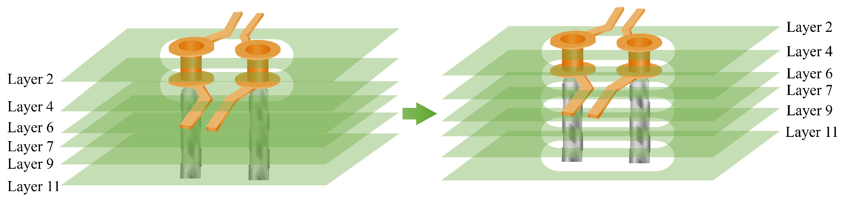
| Scheme 3 | On the basis of Scheme 1 and Scheme 2, the radius of the VIAs and anti-pads and the length of back-drill all remained unchanged, then anti-pads were added in the part troughed by the back-drill. The influence on the S-parameter was investigated. |
| Plane | Type |
|---|---|
| Layer 1/12 | Signal Plane |
| Layer 2/11 | Power Plane |
| Layer 3/10 | Signal Plane |
| Layer 4/9 | Power Plane |
| Layer 5/8 | Signal Plane |
| Layer 6/7 | Power Plane |
Disclaimer/Publisher’s Note: The statements, opinions and data contained in all publications are solely those of the individual author(s) and contributor(s) and not of MDPI and/or the editor(s). MDPI and/or the editor(s) disclaim responsibility for any injury to people or property resulting from any ideas, methods, instructions or products referred to in the content. |
© 2024 by the authors. Licensee MDPI, Basel, Switzerland. This article is an open access article distributed under the terms and conditions of the Creative Commons Attribution (CC BY) license (https://creativecommons.org/licenses/by/4.0/).
Share and Cite
Xu, W.-J.; Xin, D.-J.; Yang, L.; Zhou, Y.-K.; Wang, D.; Li, W.-X. High-Speed Signal Optimization at Differential VIAs in Multilayer Printed Circuit Boards. Electronics 2024, 13, 3377. https://doi.org/10.3390/electronics13173377
Xu W-J, Xin D-J, Yang L, Zhou Y-K, Wang D, Li W-X. High-Speed Signal Optimization at Differential VIAs in Multilayer Printed Circuit Boards. Electronics. 2024; 13(17):3377. https://doi.org/10.3390/electronics13173377
Chicago/Turabian StyleXu, Wen-Jie, Dong-Jin Xin, Lei Yang, Yong-Kang Zhou, Dong Wang, and Wei-Xin Li. 2024. "High-Speed Signal Optimization at Differential VIAs in Multilayer Printed Circuit Boards" Electronics 13, no. 17: 3377. https://doi.org/10.3390/electronics13173377