Article

Analysis of the Second-Order NS SAR ADC Performance Enhancement Based on Active Gain

1
School of Integrated Circuits, University of Chinese Academy of Sciences, Beijing 100049, China
2
Institute of Microelectronics of the Chinese Academy of Sciences, Beijing 100029, China
*
Author to whom correspondence should be addressed.
Electronics 2024, 13(17), 3400; https://doi.org/10.3390/electronics13173400
Submission received: 17 July 2024 / Revised: 17 August 2024 / Accepted: 22 August 2024 / Published: 27 August 2024

Abstract

:
This paper presents a novel second-order passive noise shaping (NS) successive approximation register (SAR) analog-to-digital converter (ADC) based on active gain. The proposed scheme achieves a further improvement in the signal-to-noise ratio (SNR) of the proposed NS SAR ADC by reducing the kT/C noise and the conversion rate. After having presented the conversion principle, the theoretical analysis of the performance enhancement based on noise and other considerations is presented.

1. Introduction

The successive approximation register (SAR) analog-to-digital converter (ADC) is one of the most widely used ADC architectures. It offers medium resolution and is simple to design [1,2,3,4]. However, for high-resolution applications, its power efficiency degrades due to stringent requirements on the comparator noise and the exponentially growing capacitor digital-to-analog converter (DAC) array. The noise shaping (NS) SAR ADC is an emerging hybrid ADC architecture that combines the advantages of SAR and Sigma–Delta ADCs [5,6,7,8]. The NS SAR ADC significantly reduces in-band comparator noise and quantization noise without degrading power efficiency [9,10]. Comparator noise is a critical factor in signal-to-noise ratio (SNR). Due to the simple structure and lower power consumption of dynamic comparators, they are more widely used in SAR ADCs than the static comparator. However, the input referred noise of dynamic comparators is larger than static comparators because of its low gain. Although the comparator noise is shaped in NS SAR ADC, it remains too large for high-resolution systems. Several methods have been proposed to minimize it. The SNR and spurious free dynamic range (SFDR) enhancement technique is proposed [11,12,13], repeating comparison of least significant bit (LSB) by using redundant DAC to average comparator noise. To effectively reduce the comparator noise and increase its lower-bits decision accuracy, the majority voting (MV) technique is proposed [14,15], and a tri-level voting technique is employed [16]. However, these techniques come at the expense of a lower sampling rate.
Although NS SAR ADCs can also reduce the number of quantizer bits, the kT/C noise decreases as the capacitance increases. Therefore, increasing the capacitor array is essential for high-resolution applications. There are three drawbacks associated with a large capacitance. The first, a large capacitance means a large area, which burdens the whole chip. Second, a larger capacitance consumes more dynamic power. Third, a large sampling capacitance also increases the power consumption of the input buffer. Therefore, increasing the capacitance may not be an effective way to reduce the kT/C noise. To overcome the limitations of the large capacitance and the input-referred noise of the dynamic comparator, this paper proposes a second-order NS SAR ADC based on active gain. The proposed method achieves a further improvement in the SNR of NS SAR ADC and sampling speed while using the smaller capacitance. This paper provides a mathematical analysis of the noise and non-ideal factors demonstrating the effectiveness of the proposed scheme.
This paper is organized as follows. Section 2 presents a mathematical analysis of previous second-order fully-passive NS SAR ADC architecture. Section 3 discusses the two schemes of proposed second-order NS SAR ADC based on active gain. Section 4 compares the advantages and disadvantages of the proposed schemes. Section 5 concludes this paper.

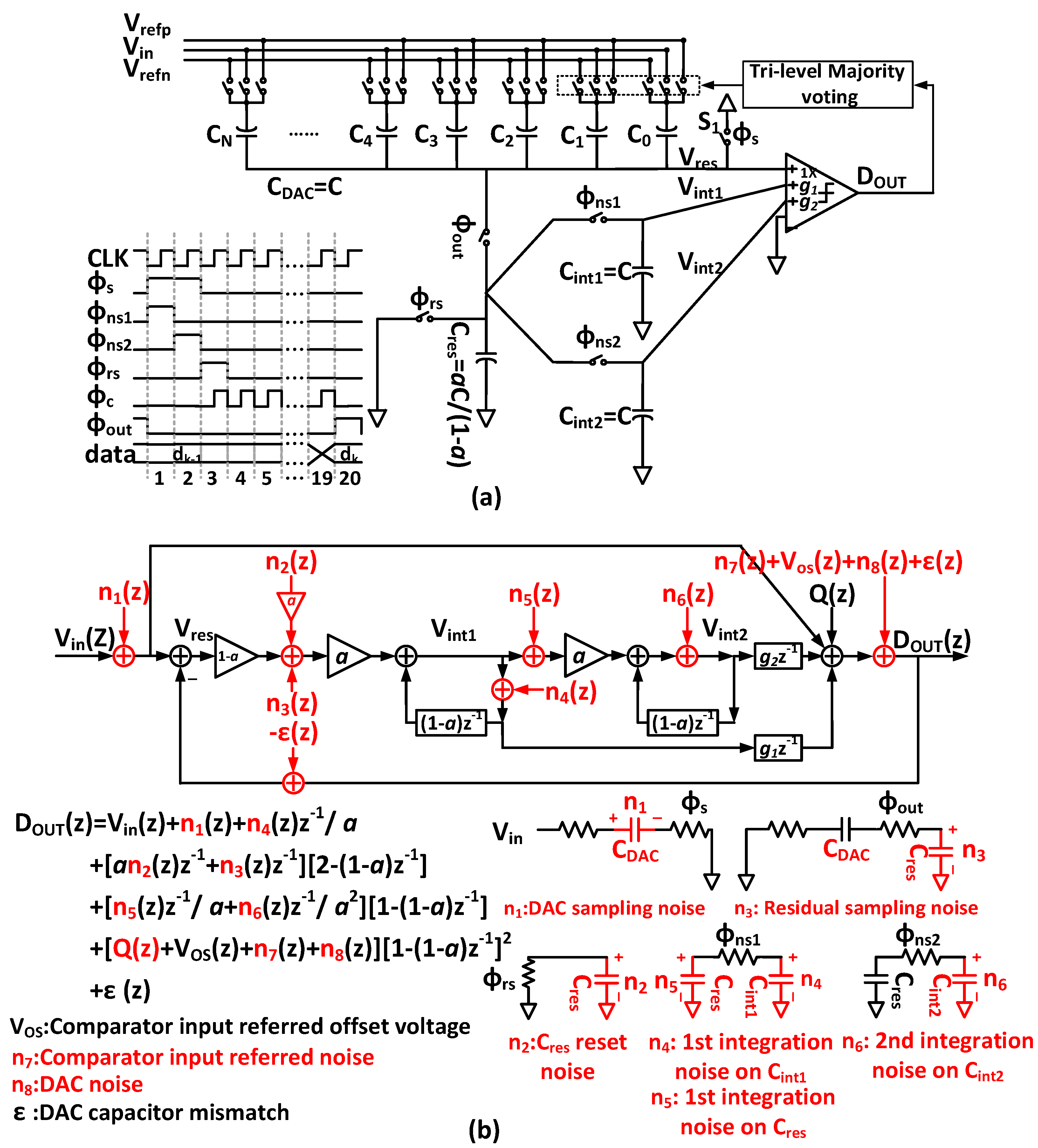
2. Mathematical Analysis of Previous Second-Order Fully-Passive NS SAR ADC

Some prior works utilized operational transconductance amplifiers (OTA) to construct active filters, which can achieve good NS effect [9]. However, OTA consumes high power and is scaling-unfriendly. In recent years, methods utilizing switches and capacitors to implement fully passive filters have been proposed [17,18]. These passive switched capacitor filters are simple, low power, robust, and scaling-friendly. The previous second-order fully-passive NS SAR ADC work is shown in Figure 1 [16]. According to the signal flow diagram shown in Figure 1, Vint1 and Vint2 can be obtained:
V i n t 1 ( z ) = ( 1 a ) a 1 ( 1 a ) z 1 V r e s ( z )
and
V i n t 2 z = a 1 1 a z 1 V i n t 1 z = ( 1 a ) a 2 [ 1 1 a z 1 ] 2 V r e s ( z )
where the residual voltage is Vres(z) = Vin(z) − DOUT(z).
The relationship between input and output can be expressed as:
D O U T z = V i n z + g 1 z 1 V i n t 1 z + g 2 z 1 V i n t 2 z + Q ( z )
where Q(z) is quantization noise. By substituting (1) and (2) into (3), the z-domain transfer function with only quantization noise of the previous NS SAR ADC can be calculated as follows:
D O U T z = V i n z + [ 1 1 a z 1 ] 2 1 + 1 a g 2 a 2 + g 1 a 2 z 1 + 1 a 2 ( 1 g 1 a ) z 2 Q ( z )
The typical values of a, g1, g2, and oversampling ratio (OSR) in Figure 1 are 1/4, 4, 16, 16, respectively. The parameter a is robust against process–voltage–temperature (PVT) variations and mismatches because it depends on the ratio of the capacitance. The parameters g1 and g2 represent the strengths of different input pairs of the comparator, and they are insensitive to PVT variations and mismatches. However, the variations of g1 and g2 with PVT do not affect the stability of the structure, which has been analyzed in detail [16].
The parameters a, g1, and g2 may be affected by PVT variations and mismatches during the manufacturing process. However, a, g1, and g2 are regarded as constant in the following analysis because PVT variations and mismatches are ignored. Therefore, the z-domain transfer function including only quantization noise can be simplified as follows:
D O U T z = V i n z + [ 1 3 4 z 1 ] 2 Q ( z )
The z-domain transfer function including quantization noise and other noise is shown in Figure 1b. The signal transfer function (STF) is given by STF = 1, indicating that there is no energy loss in the signal power. For different noise sources, the noise transfer functions (NTFs) are different. The quantization noise transfer function is given by (1 − 0.75 z−1)2. The noise power n 1 2 n 6 2 are kT/C, (1 − a)kT/aC = 3 kT/C, (1 − a)2kT/aC = 2.25 kT/C, akT/C = 0.25 kT/C, (1 − a)2kT/aC = 2.25 kT/C, and akT/C = 0.25 kT/C, where k is the Boltzmann constant. Their in-band noise power will be calculated separately. In order to estimate the in-band power of the quantization noise, it is useful to find the magnitude of the quantization noise transfer function in the frequency domain by setting z = ej2πf. For frequencies that satisfy f ≪ 1, |NTF(ej2πf)| ≈ 1/16 + 3(πf)2. The in-band power of the quantization noise, PQ_ib, can be calculated as:
P Q _ i b = 2 0 1 2 O S R 1 3 4 z 1 2 2 P Q d f                       2 0 1 2 O S R 1 16 + 3 π f 2 2 P Q d f                                                         1 256 + π 2 32 1 O S R 2 + 3.6 π 4 32 1 O S R 4 P Q O S R
where PQ is the quantization noise power of the SAR ADC without NS. Ignoring considering other noises, the improved ideal effective number of bits (ENOBs), denoted as ENOBimp, can be expressed as the following expression.
E N O B i m p = 10 l o g ( 1 256 1 O S R + π 2 32 1 O S R 3 + 3.6 π 4 32 1 O S R 5 ) 6.02
When the OSR is set to 16, ENOBimp ≈ 5.76 can be obtained. Oversampling can reduce the in-band noise power by OSR times. By observing (6), it can be found that NS suppresses the low-frequency quantization noise power by approximately a factor of 256. Similar to quantization noise, comparator input-referred noise and DAC noise are also affected by the passive second-order NS.
Using similar calculations, the in-band noise powers of different noise sources can be obtained separately. The in-band noise power n 1 _ i b 2 n 6 _ i b 2 are approximately n 1 2 /OSR, [0.1 + π2/(32OSR2)] n 2 2 /OSR, [1.56 + π2/(2OSR2)] n 3 2 /OSR, 16 n 4 2 /OSR, [1 + 4π2/OSR2] n 5 2 /OSR, [16 + 64π2/OSR2] n 6 2 /OSR. It is obvious that the structure’s NS ability for different noises is not the same. If the noise is unaffected by NS, the noise power becomes 1/OSR times the original after oversampling. Since n 2 _ i b 2 is smaller than n 2 2 /OSR, the noise n2 is shaped to contribute less noise. By examining n 1 _ i b 2 n 6 _ i b 2 , it is clear that only the in-band noise powers of Cres reset noise n2, comparator input referred noise n7 and DAC noise n8 are suppressed by NS, and DAC sampling noise n1 is not affected by NS. However, the in-band noise powers of n3 − n6 are enlarged by NS. Since n1 − n6 and n8 are all kT/C noise and only n8 is second-order shaped, n1 − n6 are the primary contributors of the kT/C noise.
The kT/C noise and comparator input-referred noise n7 are the main two noise sources by mathematical analysis of previous second-order fully-passive NS SAR ADC. NS effectively suppresses the low-frequency comparator input-referred noise power, reducing it by approximately a factor of 256. In this structure, the comparator input-referred noise is suppressed by the second-order NS. However, NS achieves limited suppression of low-frequency Cres reset noise power, reducing it by about a factor of 10, while the in-band noise powers of n3 − n6 are enlarged by NS. In order to effectively reduce the kT/C noise, the capacitance must be large enough for high-resolution applications. To address this issue, the second-order NS SAR ADC based on active gain is proposed.

3. The Proposed Second-Order NS SAR ADC

In order to reduce the kT/C noise, an open-loop amplifier is used in the proposed second-order NS SAR ADC based on active gain. However, it can decrease the kT/C noise, except the DAC sampling noise. On the basis of second-order NS SAR ADC based on active gain, the improved second-order NS SAR ADC based on active gain is proposed to suppress the DAC sampling noise. Key parameters related to the amplifier need to be designed and selected reasonably for optimum noise performance. Finally, the speed issue and kickback noise issue of the proposed structures are analyzed.

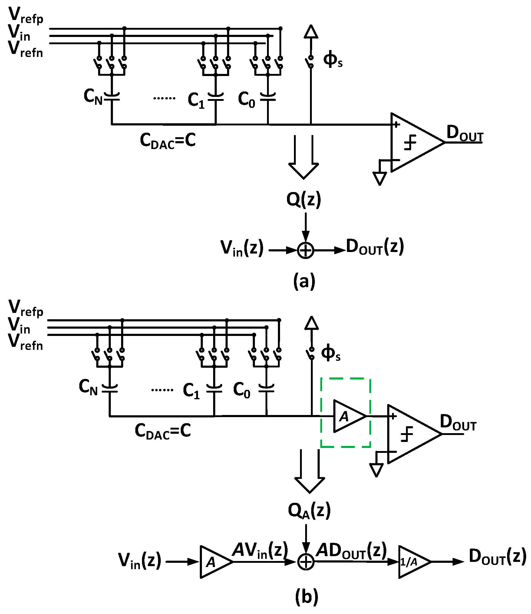
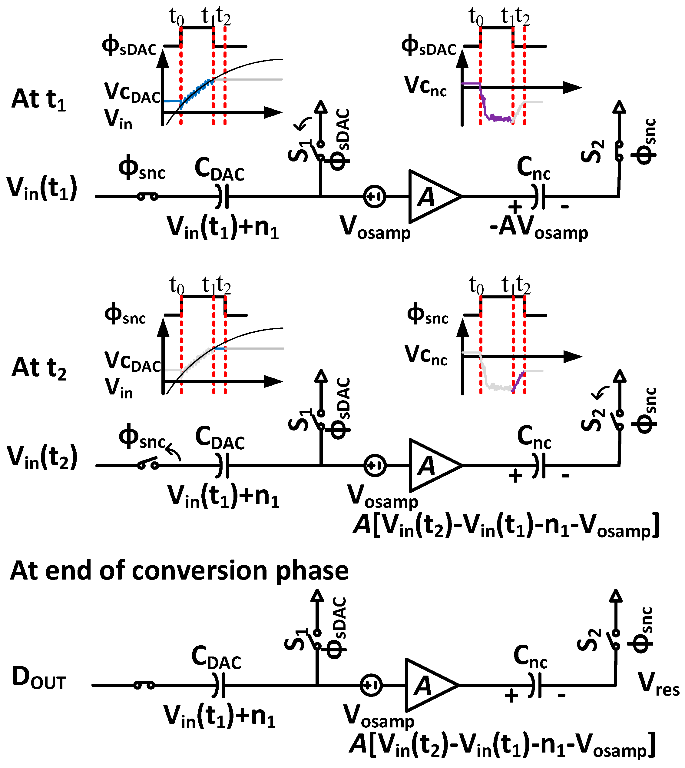
3.1. The Second-Order NS SAR ADC Based on Active Gain

The schematic and signal flow diagram of SAR ADC are shown in Figure 2a [19]. Based on the signal flow diagram, the z-domain transfer function including only quantization noise is Dout(z) = Vin(z) + Q(z). The quantization noise Q(z) can be obtained.
Q z = D o u t z V i n z
The schematic and equivalent signal flow diagram of SAR ADC based on active gain are shown in Figure 2b. An open-loop amplifier is integrated between the DAC capacitor array and the comparator. The DC gain of the open-loop amplifier is A. Based on the equivalent signal flow diagram, the quantization noise QA(z) can be obtained.
Q A z = A D o u t z V i n z = A Q z
Therefore, the z-domain transfer function including only quantization noise of SAR ADC based on active gain is:
D o u t z = V i n z + Q z
This result is the same as the transfer function of the SAR ADC, indicating that the addition of the amplifier does nothing to quantization noise. To assess the impact on other noises, the DAC sampling noise and the comparator input referred noise are added to the signal flow diagram shown in Figure 3. Since the DAC capacitor array and comparators in Figure 2a,b are identical, the DAC sampling noise n1(z) and the comparator input referred noises n7(z) remain consistent in both Figure 3a,b.
According to the signal flow diagram shown in Figure 3a, the z-domain transfer function with the DAC sampling noise and comparator input referred noise of SAR ADC is:
D o u t z = V i n z + Q z + n 1 ( z ) + n 7 ( z )
However, the z-domain transfer function with the DAC sampling noise and comparator input referred noise of SAR ADC based on active gain can be obtained based on the signal flow diagram shown in Figure 3b.
D o u t z = V i n z + Q z + n 1 ( z ) + n 7 ( z ) A
By comparing (11) and (12), It can be found that the amplifier suppresses the comparator input referred noise but not DAC sampling noise. Therefore, using the amplifier can suppress a portion of the noises, such as comparator input-referred noise, but has no influence on quantization noise and DAC sampling noise.
To mitigate the disadvantages of large capacitors, the scheme of the second-order NS SAR ADC based on active gain is proposed, as illustrated in Figure 4a. Compared to the second-order fully-passive NS SAR ADC, this scheme incorporates three additional components, which include an open-loop amplifier, a cancellation capacitor Cnc, and a sampling switch S2. Cnc must satisfy Cnc:Cres:Cint1:Cint2 = 3:1:3:3. A represents the DC gain of the open-loop amplifier. At the end of the sampling phase, the sampling switches S1 and S2 are switched off simultaneously. Hence, the offset voltage Vosamp of the amplifier can be stored on the cancellation capacitor Cnc. During the conversion phase, the final residual voltage of the DAC array is amplified by a factor of A, which decreases the effect of noise n2 − n7 and n9 on circuit performance.
In Figure 4, the residual voltage is Vres(z) = A (Vin(z) − DOUT(z)). The output voltage of the amplifier can be thought of as Vres because the voltage stored on Cnc does not change during the SAR conversion. When φout becomes high, Vres is sampled by Cres, and the voltage on Cres is (1 − a) Vres(z). When φns1 and φns2 go high, the same expressions for Vint1 and Vint2 are obtained as those in the second-order fully-passive NS SAR. Therefore, (1) and (2) can be also obtained.
Using the signal flow diagram in Figure 4b, (13) can be obtained.
A D O U T z = A V i n z + g 1 z 1 V i n t 1 z + + g 2 z 1 V i n t 2 z + A Q ( z )
(1) and (2) are substituted into (13), and the z-domain transfer function with only quantization noise of the proposed NS SAR ADC can be calculated without considering the PVT variations and mismatches of a, g1, and g2.
  D O U T z = V i n z + 1 0.75 z 1 2 Q ( z )
The comparison of (14) and (5) demonstrates that using the amplifier has no effect on quantization noise. In order to accurately describe the noise suppression advantages of the proposed scheme for other noises, the signal flow diagram and complete z-domain transfer function with all noises of the proposed NS SAR ADC are shown in Figure 4b. The STF is still 1, and the noise transfer function has been changed. The magnitude of the noise n2 − n7 and n9 is attenuated by the open-loop amplifier gain A, and the power of the noise n2− n7 and n9 is attenuated by A2. The noise n2 − n7 and n9 is related to the capacitors Cnc, Cres, Cint1, and Cint2. Therefore, the active amplifier can be used to greatly reduce the capacitance of the capacitors Cnc, Cres, Cint1, and Cint2. Both n9 and AMP input-referred noise n10 are new noise sources. The power of Cnc sampling noise n9 is kT/C. The structure of the amplifier [20] shown in Figure 4a can be employed in the proposed NS SAR ADC. The single-end input-referred noise power spectrum density (PSD) of a CMOS-input preamp is:
n 10 2 ¯ Δ f = 4 k T γ G m
where the theoretical value of γ is 2/3 for long-channel devices and Gm is the transconductance of the open-loop amplifier. The noise bandwidth of the open-loop amplifier during the sampling phase is about 1/4RoutCnc. Rout = A/Gm is the output resistance of the open-loop amplifier. Thus, the power of AMP input referred noise n10 can be calculated as:
  n 10 2 ¯ = 4 k T γ G m × 1 4 R o u t C n c = k T γ A C
It can be seen that the AMP input-referred noise power is inversely proportional to the amplifier gain A from (16). Only the noises n1 and n8 are not suppressed by A. The noise n1 directly affects the output signal and is not second-order-shaped like n8. Therefore, n1 becomes the main kT/C noise source.

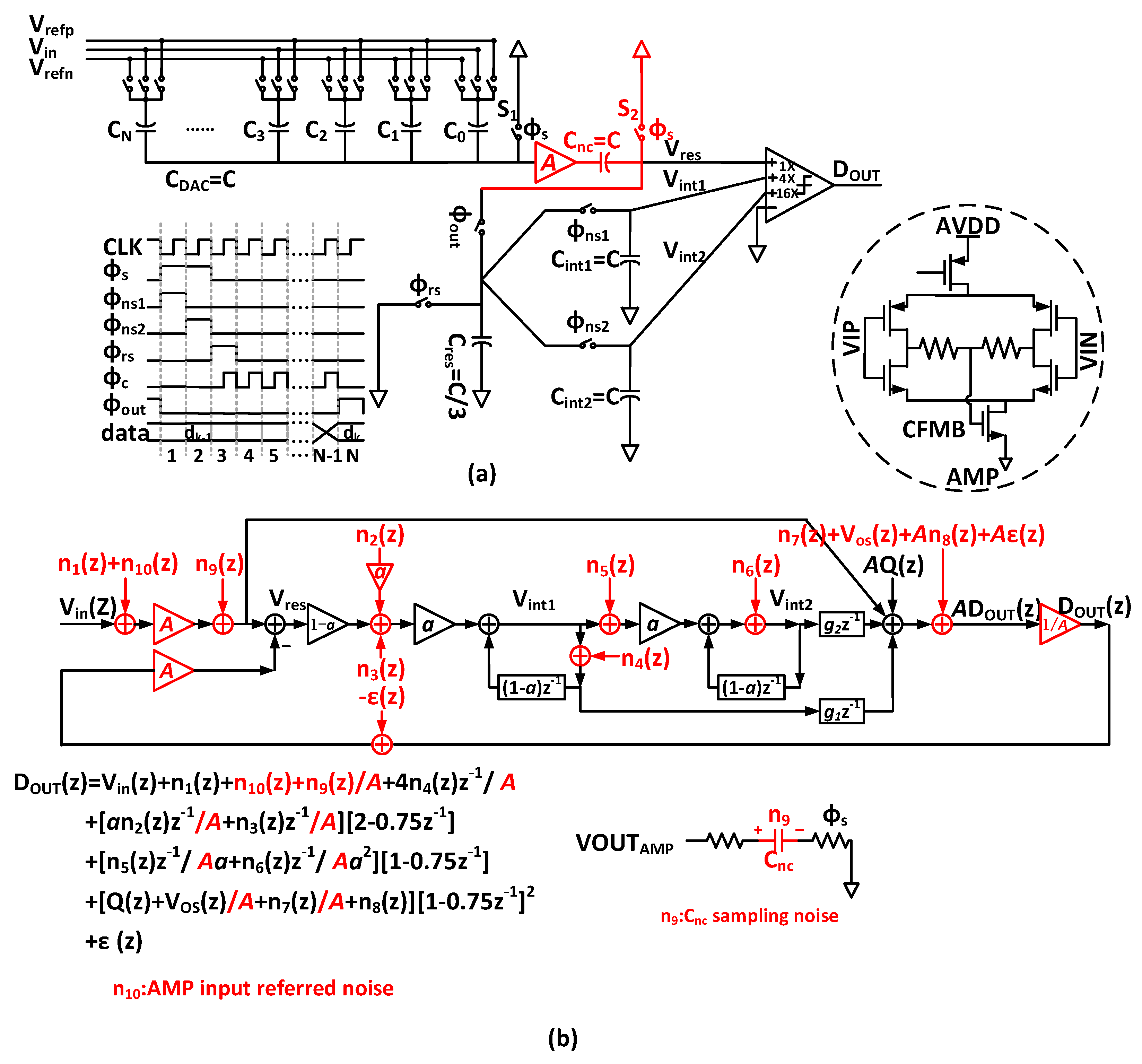
3.2. Improved Second-Order NS SAR ADC Based on Active Gain

To alleviate the deterioration of the output signal by noise n1, the improved second-order NS SAR ADC based on active gain is proposed, shown in Figure 5. The kT/C noise cancellation principle proposed by [21,22] is employed. There is a change in the timings compared to Figure 4a. φs is split into φsDAC and φsnc, controlling switches S1 and S2, respectively.
The kT/C noise cancellation principle is shown in Figure 6. The sampling phase is divided into the CDAC sampling phase and the Cnc sampling phase. The CDAC sampling phase lasts from t0 to t1 controlled by φsDAC. At the moment t1, the sampled input signal Vin(t1) and kT/C noise n1 are stored on CDAC. The offset voltage Vosamp of the amplifier is stored on the Cnc, as in Figure 4a. The Cnc sampling phase operates from t1 to t2 controlled by φsnc. At t2, the input signal is Vin(t2), and the input voltage of the amplifier is Vin(t2) − Vin(t1) − n1 − Vosamp. Assuming the amplifier has infinite bandwidth, it fully settles during the Cnc sampling phase. The voltage stored on Cnc is:
  V C n c = A [ V i n t 2 V i n t 1 n 1 V o s a m p ]
Neglecting capacitances Cint1, Cint2, and Cres, the input–output relation can be computed as (18) at the end of the conversion phase.
D O U T = V i n t 2 + V r e s / A V i n t 2
By observing (18), it can be seen that the sampling noise n1 can be completely canceled if the amplifier has an infinite bandwidth. In fact, the bandwidth of the amplifier is limited. Therefore, the sampling noise voltage stored on Cnc is:
n 1 _ C n c = A n 1 ( 1 e Δ t / τ )
where τ is the settling time constant of the amplifier [23] and the time interval satisfies Δt = t2 − t1. The voltage stored on Cnc is A[Vin(t2) − Vin(t1) − n1(1 − e−Δt/τ) − Vosamp]. The new input–output relationship can be computed as:
  D O U T = V i n t 2 + n 1 e Δ t / τ
From the above analysis, it can be concluded that kT/C noise cancellation allows the sampling noise power to be attenuated by e2Δt/τ. As a result, the z-domain transfer function of the improved second-order NS SAR ADC scheme can be expressed as follows:
D O U T = V i n z + n 1 e Δ t τ z + n 10 z + n 9 z A + n 4 z z 1 A a + a n 2 z z 1 A + n 3 z z 1 A 2 0.75 z 1   + n 5 z z 1 A a + n 6 z z 1 A a 2 1 0.75 z 1                                         + Q z + V O S A + n 7 z A + n 8 z 1 0.75 z 1 2                 + ε z                                                                                                                                          
It is possible to achieve a reduction in the overall capacitance in the improved second-order NS SAR ADC by designing the values of A and Δt/τ in a rational way. This makes it possible to use the structure in high-resolution applications where large-area capacitors are not applicable.

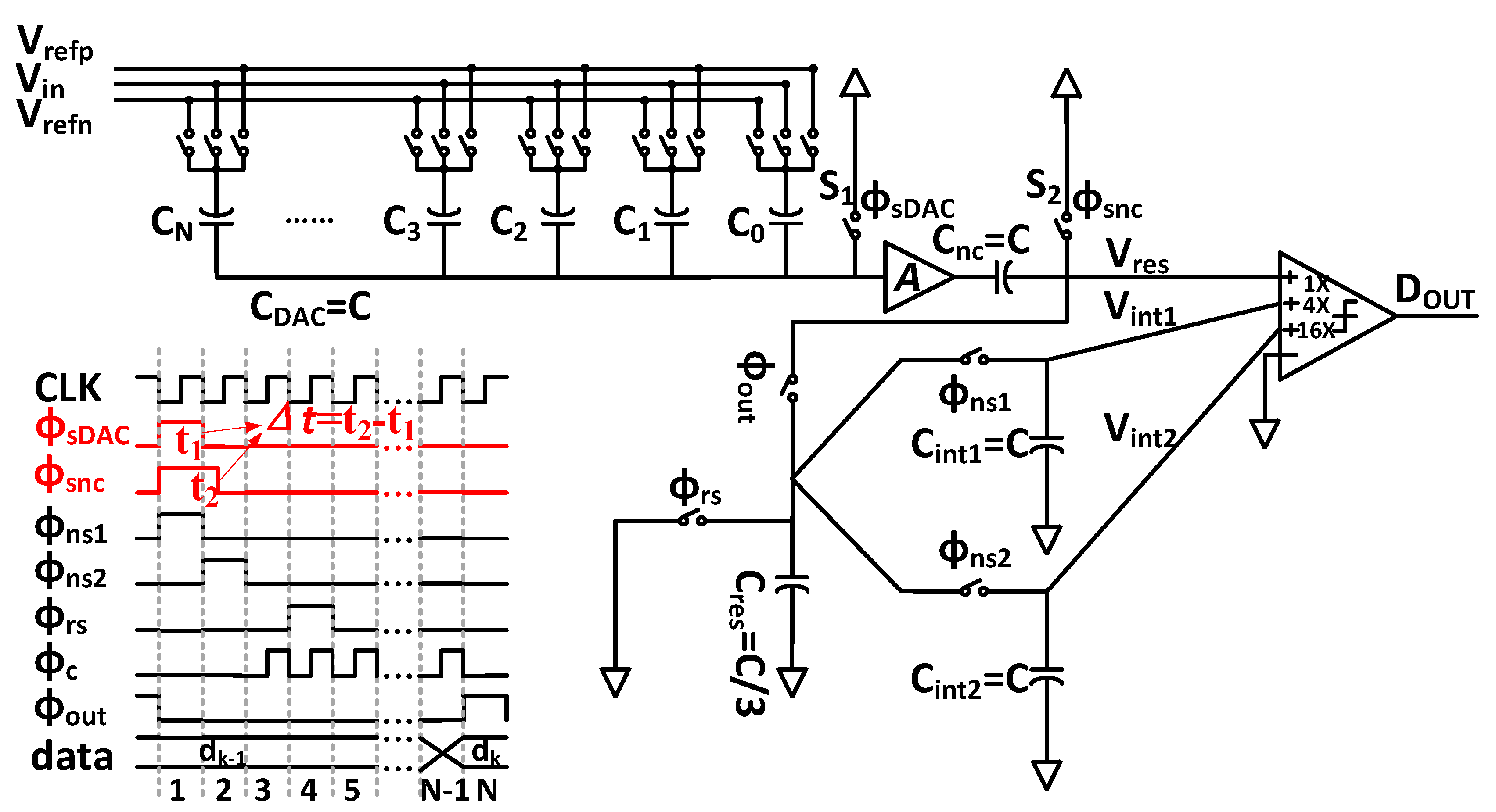
3.3. The Values of A and Δt/τ

The selection of A and Δt/τ is crucial for the attenuation of kT/C noise and the performance of the proposed scheme. If the gain A is too large, it can easily lead to saturation of the open-loop amplifier. On the contrary, if the gain A is too small, noises n2 − n7 and n9 − n10 cannot be sufficiently suppressed, resulting in little performance improvement. Therefore, the value of A must be reasonable. To ensure that the open-loop amplifier accurately amplifies the residual voltage of the DAC array generating Vres, it is necessary to ensure that (22) is satisfied.
A V i n t 2 V i n t 1 n 1 V o s a m p + A V r e s _ D A C < A V D D 2 V d s a t
where Vres_DAC is the residual voltage of the DAC array, AVDD is the power supply voltage, and Vdsat is the saturation drain voltage. In order for the amplifier to quickly remain stable in the amplification region at the end of the conversion, Vres_DAC is taken to be at least 4LSB instead of LSB (LSB = (Vrefp − Vrefn)/2N). The maximum amount of change in the input signal during the time interval Δt is:
  V i n t 2 V i n t 1 m a x s i n 2 π f i n m a x t m a x × Δ t = 2 π f i n m a x × Δ t = π f s a m × Δ t / O S R
where finmax is the maximum frequency of the input signal, fsam is the sampling frequency, and finmax = fsam/2OSR. n1 is the DAC sampling noise voltage with a noise power of kT/CDAC. Thus, the distribution of n1 is N (0, √kT/CDAC). The maximum value of n1 can be considered:
| n 1 | m a x = 5 k T / C D A C
The maximum gain can be calculated as follows:
  A m a x = A V D D 2 V d s a t π f s a m O S R × Δ t + 5 k T C D A C + V o s a m p m a x + 4 L S B
In order to minimize sampling noise without increasing the array of sampling capacitors CDAC, the value of Δt/τ needs to be as large as possible. However, it is clear that an increase in Δt leads to a decrease in A and sampling speed. Reducing τ will increase power consumption and improve sampling speed. Therefore, the value of Δt/τ cannot be too large. This requires a compromise between noise performance, power consumption, and speed.

3.4. Improved Sampling Speed
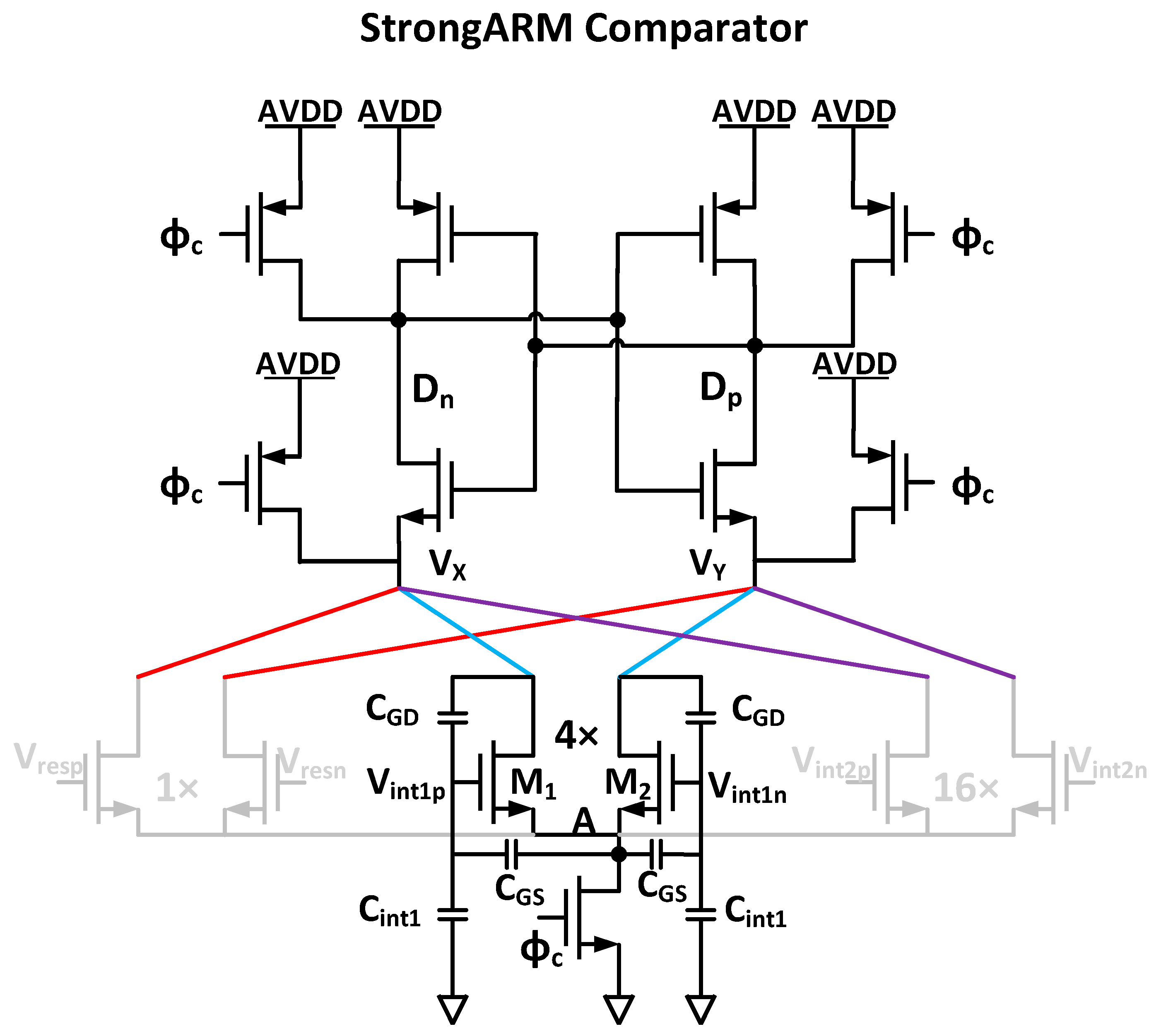
The structure of the three-path dynamic strong-arm comparator can be used in the proposed improved second-order NS SAR ADC scheme shown in Figure 7. The widths of the three input pairs are W, 4 W, and 16 W. Compared to a classic one-path comparator, which has the same total input pair width of 21 W, the noise referred to the 1× path of the three-path comparator is 21 times larger but it is attenuated by 16 times due to NS. As a result, the in-band noise of the three-path comparator is 21/16 times larger than that of the one-path comparator. Therefore, the noise of the three-path comparator is still relatively large for high-resolution applications. In a word, the second-order fully-passive NS SAR ADC, which mainly reduces the quantization noise from (5), does not bring any benefits to the comparator noise. To improve the SNR, reducing the comparator noise is necessary. For example, the NS SAR [14] performs a single comparison for the first 9 bits (including 1 redundant bit) and only performs repeated comparisons for the LSB bit, which reduces the sampling rate by almost half. However, the technique proposed in this paper not only reduces the kT/C noise but also reduces the comparator noise n7 from (21). The proposed technique has no extra cycles to average the comparator noise but increases the power consumption of an amplifier. A compromise between power consumption and speed is needed for the designer.

3.5. Kickback Noise

A three-path dynamic strong-arm comparator is shown in Figure 7. This is a strong-arm latch with three input pairs. The summation of the input voltage is realized by merging the currents of input pairs, which are controlled by the input voltage. The summation is controlled by the clock and does not require a static analog adder. However, Vres, Vint1, and Vint2 need a fixed voltage gain ratio of 1:4:16. Because passive integrators do not provide voltage gain, it is best that the comparator provides the voltage gain ratio. Therefore, it is optimal for this comparator to have three input pairs. As a result, the relative gains can be realized by sizing the input pairs of the comparator into specific ratios. Setting the voltage gain ratio by sizing the input pairs is beneficial for PVT variation and mismatch. This does not require the involvement of amplifiers, which reduces the circuit complexity and saves power consumption.
The comparator is reset when φc is low. Dn, Dp, Vx, and VY are AVDD. When φc is high, Vx and VY begin to vary, resulting in one of Dn and Dp becoming low. The large voltage variations of Vx and VY are coupled through the parasitic capacitances of the input transistors to the input of the comparator. The input voltage will be disturbed, which will worsen the accuracy of the comparator. This disturbance is usually called kickback noise [24]. The kickback noise includes common noise and differential noise. The common kickback noise is coupled through CGS (assume CGS1 = CGS2 = CGS). The common kickback noise can usually be ignored since it has a common coupling point. The differential kickback noise is related to the difference VX−Y between VX and VY, as well as the ratio of CGD to Cint1 using the 4× path as an example. The detailed analysis of VX−Y is shown in [25]. Assume CGD1 = CGD2 = CGD; the differential kickback noise εk can be approximately expressed as:
  ε k C G D C i n t 1 + C G D V X Y C G D C i n t 1 V X Y
Thus, the reduction in capacitance leads to a degradation of the kickback noise. If Cint1 shrinks by a factor of A2, the new kickback noise εk’ will be approximately A2εk. The input referred to as kickback noise is about Aεk. If the capacitance is too small, the kickback noise will be the dominant noise. The kickback noise needs to be optimized when the capacitance becomes smaller. On the one hand, the size of the input transistors is optimized to reduce the parasitic capacitance CGD. On the other hand, there is a trade-off between capacitance and kickback noise.

4. Performance Comparison

For the purpose of facilitating comparison, the single-ended second-order fully-passive NS SAR ADC, NS SAR ADC based on gain, and improved NS SAR ADC based on gain are equipped with three-path dynamic strong-arm comparators and only the effect of kT/C thermal noise on SNR is considered. In order to achieve the same SNR, the three different structures require different capacitance sizes. Therefore, N-bit binary weighted DACs (unit capacitance may vary) are used [26]. For the second-order fully-passive NS SAR ADC, the input capacitance is the total capacitance of N-bit binary weighted DAC. Thus, the input capacitance of the second-order fully-passive NS SAR ADC, named Cit, is:
  C i t = 2 N C 0
where C0 is the unit capacitance of the second-order fully-passive NS SAR ADC.
The ratio between the input capacitance and the integrating capacitance is Cit:Cres:Cint1:Cint2 = 3:1:3:3, shown in Figure 1a. Hence, the total capacitance of the second-order fully-passive NS SAR ADC, named Ctt, can be obtained.
  C t t = 10 × 2 N C 0 3
An open-loop amplifier is introduced in the structure of NS SAR ADC based on active gain. Meanwhile, a cancellation capacitor Cnc is introduced. The structure of NS SAR ADC based on active gain does not adopt the kT/C noise cancellation technique. In order to obtain the same SNR, the minimal input capacitance, named Cig_m, is:
  C i g _ m = 2 N C 0
Observing the z-domain transfer function of NS SAR ADC based on active gain, it can be known that the noise powers of n2 − n6 and n9 associated with Cnc, Cres, Cint1, and Cint2 are suppressed by the gain A2. Therefore, Cres, Cint1, and Cint2 can all be approximately scaled down by a factor of A2 compared to that of the second-order fully-passive NS SAR ADC. The ratio of the integrating capacitances is Cnc:Cres:Cint1:Cint2 = 3:1:3:3. Therefore, the minimal total capacitance of NS SAR ADC based on active gain, named Ctg_m, can be approximately expressed.
C t g _ m 2 N C 0 + 10 × 2 N C 0 3 × 1 A 2 2 N C 0 ( 10 3 A 2 + 1 )
On the basis of the structure of NS SAR ADC based on active gain, the kT/C noise cancellation technique is introduced into the structure of improved NS SAR ADC based on active gain. It can be found that the DAC sampling noise is suppressed by a factor of eΔt/τ from (21). In other words, the DAC sampling noise power is suppressed by a factor of e2Δt/τ. The input capacitance of the structure of improved NS SAR ADC based on active gain can be reduced by a factor of e2Δt/τ compared to that of the second-order fully-passive NS SAR in order to obtain the same SNR. Therefore, the minimal input capacitance of the structure of improved NS SAR ADC, named Ciig_m, is:
C i i g _ m 2 N C 0 e 2 Δ t / τ
Therefore, the minimal total capacitance of improved NS SAR ADC based on active gain, named Ctig_m, can be approximately expressed as follows:
C t i g _ m 2 N C 0 ( 10 3 A 2 + 1 e 2 Δ t / τ )
In order to compare (27) and (28) and (29)–(32), the expressions all contain C0, which is the unit capacitance of the second-order fully-passive NS SAR ADC. However, this does not mean that the unit capacitance of NS SAR ADC based on active gain and improved NS SAR ADC based on gain is C0, and the unit capacitance of NS SAR ADC based on active gain and improved NS SAR ADC based on gain can be reasonably assigned based on the total capacitance and input capacitance.
The minimal Ctotal and input cap are shown by (27)–(32). However, non-ideal factors will limit the Ctotal and input cap in the process of circuit implementation, especially the Ctotal. Taking the kickback noise as an example, if Cint1 is reduced by A2 times, the input-referred kickback noise associated with Cint1 will be increased by about A times from (26). If Cint1, Cint2, Cres, and Cnc are all reduced by A2 times, the input-referred kickback noise will be increased by about A times. Worsened kickback noise may lead to the deterioration of the SNR. This will limit Cint1 from shrinking by a factor of A2, which results in Ctotal not reaching the minimal Ctotal. Moreover, the influence of non-ideal factors such as clock feedthrough and charge injection will gradually increase with the decrease in Ctotal. Therefore, the selection of Ctotal also needs to consider the influence of non-ideal factors in the circuit implementation. However, even considering non-ideal factors, the Ctotal of second-order fully-passive NS SAR is large, and the Ctotal of improved NS SAR ADC base is small when the same SNR is achieved. Compared to the other two structures’ Ctotal, the Ctotal of NS SAR based on active gain is medium. The capacitance value reflects the circuit’s ability to suppress kT/C noise. The smaller the capacitance used to achieve the same performance, the better the circuit performance of suppressing kT/C noise. Therefore, capacitance is also an important parameter for SAR ADCs. Only the architecture of improved NS SAR ADC based on gain adopts the kT/C noise cancellation technique, so the input capacitance of this structure is minimal. This alleviates the difficulty of designing the input buffer. Active gain is introduced in the structures of NS SAR ADC based on gain and improved NS SAR ADC based on gain to decrease the comparator noise and the kT/C noise excluding kT/C sampling noise. The comparator noise is suppressed by the open-loop amplifier, which makes it unnecessary to use extra clock cycles to reduce the comparator noise. This improves the sample rate, which is a parameter characterizing the speed of the ADC. However, the open-loop amplifier used in the proposed architectures also consumes static power, which is not friendly to the overall power consumption and Schreier Figure of Merit (FoM) or Walden FoM. Therefore, power consumption is also an important parameter to compare. Performance comparison and summary of the single-ended second-order fully-passive NS SAR ADC, NS SAR ADC based on gain and improved NS SAR ADC based on gain is shown in Table 1.

5. Conclusions

This paper proposes a novel second-order passive NS SAR ADC based on active gain, which effectively suppresses the negative effect of kT/C on SNR. Compared to the second-order fully-passive NS SAR ADC, an open-loop amplifier, a cancellation capacitor Cnc, and Cnc sampling switch S2 are added to the proposed scheme. The open-loop amplifier mitigates both kT/C noise and comparator noise, improving sampling speed while significantly reducing capacitance. Although smaller capacitance leads to reduced dynamic power consumption, the introduction of the open-loop amplifier results in static power consumption. This necessitates a trade-off between performance and power consumption. However, this scheme is still a good choice for high-speed and high-resolution applications.

Author Contributions

Conceptualization, S.J. and S.X.; methodology, S.J.; software, S.J.; formal analysis, S.J.; data curation, S.J.; writing—original draft preparation, S.J.; writing—review and editing, T.Y. and S.X. All authors have read and agreed to the published version of the manuscript.

Funding

This research received no external funding.

Data Availability Statement

Data are contained within the article.

Conflicts of Interest

The authors declare no conflicts of interest.

References

  1. Elzakker, M.v.; Tuijl, E.v.; Geraedts, P.; Schinkel, D.; Klumperink, E.A.M.; Nauta, B. A 10-bit Charge-Redistribution ADC Consuming 1.9 μW at 1 MS/s. IEEE J. Solid-State Circuits 2010, 45, 1007–1015. [Google Scholar] [CrossRef]
  2. Liu, C.C.; Chang, S.J.; Huang, G.Y.; Lin, Y.Z.; Huang, C.M. A 1V 11fJ/conversion-step 10bit 10MS/s asynchronous SAR ADC in 0.18µm CMOS. In Proceedings of the 2010 Symposium on VLSI Circuits, Honolulu, HI, USA, 16–18 June 2010; pp. 241–242. [Google Scholar]
  3. Shen, Y.; Tang, X.; Shen, L.; Zhao, W.; Xin, X.; Liu, S.; Zhu, Z.; Sathe, V.S.; Sun, N. A 10-bit 120-MS/s SAR ADC With Reference Ripple Cancellation Technique. IEEE J. Solid-State Circuits 2020, 55, 680–692. [Google Scholar] [CrossRef]
  4. Xu, D.G.; Xu, K.K.; Xu, S.L.; Liu, L.; Liu, T. A System-Level Correction SAR ADC with Noise-Tolerant Technique. J. Circuits Syst. Comput. 2018, 27, 1850202. [Google Scholar] [CrossRef]
  5. Obata, K.; Matsukawa, K.; Miki, T.; Tsukamoto, Y.; Sushihara, K. A 97.99 dB SNDR, 2 kHz BW, 37.1 µW noise-shaping SAR ADC with dynamic element matching and modulation dither effect. In Proceedings of the 2016 IEEE Symposium on VLSI Circuits (VLSI-Circuits), Honolulu, HI, USA, 15–17 June 2016; pp. 1–2. [Google Scholar]
  6. Shu, Y.S.; Kuo, L.T.; Lo, T.Y. An Oversampling SAR ADC With DAC Mismatch Error Shaping Achieving 105 dB SFDR and 101 dB SNDR Over 1 kHz BW in 55 nm CMOS. IEEE J. Solid-State Circuits 2016, 51, 2928–2940. [Google Scholar] [CrossRef]
  7. Chen, Z.; Miyahara, M.; Matsuzawa, A. A 2nd order fully-passive noise-shaping SAR ADC with embedded passive gain. In Proceedings of the 2016 IEEE Asian Solid-State Circuits Conference (A-SSCC), Toyama, Japan, 7–9 November 2016; pp. 309–312. [Google Scholar]
  8. Li, S.; Qiao, B.; Gandara, M.; Pan, D.Z.; Sun, N. A 13-ENOB Second-Order Noise-Shaping SAR ADC Realizing Optimized NTF Zeros Using the Error-Feedback Structure. IEEE J. Solid-State Circuits 2018, 53, 3484–3496. [Google Scholar] [CrossRef]
  9. Fredenburg, J.A.; Flynn, M.P. A 90-MS/s 11-MHz-Bandwidth 62-dB SNDR Noise-Shaping SAR ADC. IEEE J. Solid-State Circuits 2012, 47, 2898–2904. [Google Scholar] [CrossRef]
  10. Guo, W.; Zhuang, H.; Sun, N. A 13b-ENOB 173dB-FoM 2nd-order NS SAR ADC with passive integrators. In Proceedings of the 2017 Symposium on VLSI Circuits, Kyoto, Japan, 5–8 June 2017; pp. C236–C237. [Google Scholar]
  11. Miki, T.; Morie, T.; Matsukawa, K.; Bando, Y.; Okumoto, T.; Obata, K.; Sakiyama, S.; Dosho, S. A 4.2 mW 50 MS/s 13 bit CMOS SAR ADC With SNR and SFDR Enhancement Techniques. IEEE J. Solid-State Circuits 2015, 50, 1372–1381. [Google Scholar] [CrossRef]
  12. Kuo, H.L.; Lu, C.W.; Chen, P. An 18.39 fJ/Conversion-Step 1-MS/s 12-bit SAR ADC With Non-Binary Multiple-LSB-Redundant and Non-Integer-and-Split-Capacitor DAC. IEEE Access 2021, 9, 5651–5669. [Google Scholar] [CrossRef]
  13. Jiao, Z.; Luo, H.; Zhang, J.; Wang, X.; Chen, L.; Zhang, H. An 84dB-SNDR 1-0 Quasi-MASH NS SAR with LSB Repeating and 12-bit Bridge-Crossing Segmented CDAC. In Proceedings of the 2023 IEEE Custom Integrated Circuits Conference (CICC), San Antonio, TX, USA, 23–26 April 2023; pp. 1–2. [Google Scholar]
  14. Harpe, P.; Cantatore, E.; Roermund, A.v. A 10b/12b 40 kS/s SAR ADC with Data-Driven Noise Reduction Achieving up to 10.1b ENOB at 2.2 fJ/Conversion-Step. IEEE J. Solid-State Circuits 2013, 48, 3011–3018. [Google Scholar] [CrossRef]
  15. Hwang, Y.H.; Song, Y.; Park, J.E.; Jeong, D.K. A Fully Passive Noise-Shaping SAR ADC Utilizing Last-Bit Majority Voting and Cyclic Dynamic Element Matching Techniques. IEEE Trans. Very Large Scale Integr. (VLSI) Syst. 2022, 30, 1381–1390. [Google Scholar] [CrossRef]
  16. Zhuang, H.; Guo, W.; Liu, J.; Tang, H.; Zhu, Z.; Chen, L.; Sun, N. A Second-Order Noise-Shaping SAR ADC with Passive Integrator and Tri-Level Voting. IEEE J. Solid-State Circuits 2019, 54, 1636–1647. [Google Scholar] [CrossRef]
  17. Chen, Z.; Miyahara, M.; Matsuzawa, A. A 9.35-ENOB, 14.8 fJ/conv.-step fully-passive noise-shaping SAR ADC. In Proceedings of the 2015 Symposium on VLSI Circuits (VLSI Circuits), Kyoto, Japan, 17–19 June 2015; pp. C64–C65. [Google Scholar]
  18. Guo, W.; Sun, N. A 12b-ENOB 61µW noise-shaping SAR ADC with a passive integrator. In Proceedings of the ESSCIRC Conference 2016: 42nd European Solid-State Circuits Conference, Lausanne, Switzerland, 12–15 September 2016; pp. 405–408. [Google Scholar]
  19. Kandala, M.; Sekar, R.; Chenglong, Z.; Haibo, W. A low power charge-redistribution ADC with reduced capacitor array. In Proceedings of the 2010 11th International Symposium on Quality Electronic Design (ISQED), San Jose, CA, USA, 22–24 March 2010; pp. 44–48. [Google Scholar]
  20. Zhan, M.; Jie, L.; Tang, X.; Sun, N. A 0.004mm2 200MS/S Pipelined SAR ADC with kT/C Noise Cancellation and Robust Ring-Amp. In Proceedings of the 2022 IEEE International Solid-State Circuits Conference (ISSCC), San Francisco, CA, USA, 20–26 February 2022; pp. 164–166. [Google Scholar]
  21. Liu, J.; Tang, X.; Zhao, W.; Shen, L.; Sun, N. A 13-bit 0.005-mm2 40-MS/s SAR ADC With kT/C Noise Cancellation. IEEE J. Solid-State Circuits 2020, 55, 3260–3270. [Google Scholar] [CrossRef]
  22. Li, H.; Youssef, M.; Shen, Y.; Cantatore, E.; Harpe, P. Analysis of the Sampling Noise Cancellation Technique in a Track-and-Hold Amplifier. In Proceedings of the 2021 28th IEEE International Conference on Electronics, Circuits, and Systems (ICECS), Dubai, United Arab Emirates, 28 November–1 December 2021; pp. 1–5. [Google Scholar]
  23. Xu, K. Silicon electro-optic micro-modulator fabricated in standard CMOS technology as components for all silicon monolithic integrated optoelectronic systems*. J. Micromech. Microeng. 2021, 31, 054001. [Google Scholar] [CrossRef]
  24. Figueiredo, P.M.; Vital, J.C. Kickback noise reduction techniques for CMOS latched comparators. IEEE Trans. Circuits Syst. II Express Briefs 2006, 53, 541–545. [Google Scholar] [CrossRef]
  25. Razavi, B. The StrongARM Latch [A Circuit for All Seasons]. IEEE Solid-State Circuits Mag. 2015, 7, 12–17. [Google Scholar] [CrossRef]
  26. Wu, K.J.; Li, J.; Wang, X.Z.; Ning, N.; Xu, K.K.; Yu, Q. Switching sequence optimization for gradient errors compensation in the current-steering DAC design. Microelectron. J. 2020, 95, 104662. [Google Scholar] [CrossRef]
Figure 1. Previous NS SAR ADC work. (a) Second-order fully-passive NS SAR ADC architecture. (b) Signal flow diagram.
Electronics 13 03400 g001
Figure 2. (a) Schematic and signal flow diagram of SAR ADC. (b) Schematic and equivalent signal flow diagram of SAR ADC based on active gain.
Electronics 13 03400 g002
Figure 3. (a) Signal flow diagram with the DAC sampling noise and comparator input referred noise of SAR ADC. (b) Equivalent signal flow diagram with the DAC sampling noise and comparator input referred noise of SAR ADC based on active gain.
Electronics 13 03400 g003
Figure 4. Proposed second-order NS SAR ADC scheme. (a) Second-order NS SAR ADC based on active gain. (b) Signal flow diagram.
Electronics 13 03400 g004
Figure 5. Improved second-order NS SAR ADC scheme.
Electronics 13 03400 g005
Figure 6. The kT/C noise cancellation principle.
Electronics 13 03400 g006
Figure 7. Three-path dynamic strong-arm comparator.
Electronics 13 03400 g007
Table 1. Performance comparison and summary.
ArchitectureSecond-Order Fully-Passive NS SARNS SAR Based on Active GainImproved NS SAR Based on Activegain
Ctotallargemediumsmall
ADC Input Cap 2 N C 0 2 N C 0 2 N C 0 e 2 Δ t / τ
kT/C Suppressed?×
Comparator Noise Suppressed?
Extra Cycles?××
Static Power×
Disclaimer/Publisher’s Note: The statements, opinions and data contained in all publications are solely those of the individual author(s) and contributor(s) and not of MDPI and/or the editor(s). MDPI and/or the editor(s) disclaim responsibility for any injury to people or property resulting from any ideas, methods, instructions or products referred to in the content.

