Article

Performance Analysis and Optimization of Switch Device for VLF Communication Synchronous Tuning System Based on Coupled Inductors

by
Shize Wei
,
Xu Xie
* and
Hao Zuo
College of Electronics Engineering, Naval University of Engineering, Wuhan 430030, China
*
Author to whom correspondence should be addressed.
Electronics 2024, 13(17), 3457; https://doi.org/10.3390/electronics13173457
Submission received: 30 July 2024 / Revised: 25 August 2024 / Accepted: 28 August 2024 / Published: 30 August 2024
(This article belongs to the Special Issue Advances in Electronics, Communication, and Automation)

Abstract

:
The very low frequency (VLF) communication system is characterized by a limited transmit bandwidth. Due to the low operating frequency, the dimensions of VLF antennas are significantly smaller than the corresponding wavelength. Therefore, VLF antennas are considered electrically small antennas (ESAs) with high Q values and narrow bandwidth. To achieve broadband VLF communication, synchronous tuning technology is commonly employed. In this study, we focus on analyzing the performance of the switching device in the synchronous tuning system using coupled inductors and IGBT as core components. By considering the equivalent circuit of the controlled source associated with coupled inductors, we propose an adaptive input impedance optimization algorithm based on the variable capacitor (hereinafter referred to as VC-ADIO) to address issues arising from coupling coefficient variations and internal parameters within IGBTs that affect primary loop input impedance. The radiated power of the VLF antenna is improved effectively.

1. Introduction

A VLF antenna is an electrically small antenna that satisfies the criteria proposed by Wheeler [1].
In Equation (1), l represents the maximum geometric size of the antenna, while λ denotes the operating wavelength.
For ESAs, even a slight deviation in frequency can lead to a significant alteration in the antenna’s input impedance. Since the real part of the input impedance is small, while the imaginary part is large, ESAs have a high Q factor. The Q factor of small antennas can be expressed as the reciprocal of the bandwidth, denoted as Q f 0 / ( 2 Δ f ) . Therefore, narrow bandwidth is its inherent characteristic [2].
The primary signal source for VLF communication systems is predominantly the MSK signal source because the modulation method used in very low-frequency communication must meet the following requirements: (1) The required signal-to-noise ratio should be minimized as much as possible. (2) The power utilization rate should be as high as possible. (3) The utilization rate of the frequency band should be as high as possible. (4) The transmitter adopts a phase continuous modulation method. (5) The channel envelope remains constant [3].
l λ 1 2 π
The expression of the MSK signal is [4] as follows:
S M S K = c o s ( 2 π f c t + π a k 2 T s t + φ k ) , ( k 1 ) T s t k T s
In Equation (2), f c represents the carrier frequency; T s represents the symbol width; a k represents the phase constant of the k-th symbol. When a k = + 1 , the signal frequency is f h = f c + 1 / 4 T s , and when a k = 1 , the signal frequency is f l = f c 1 / 4 T s . The symbol rate is R B = 1 / T s . In this article, f h refers to the ‘mark’ frequency and f h refers to the ‘space’ frequency.
In order to enhance the effective bandwidth and optimize the communication rate of the VLF system, two primary approaches can be employed. One involves augmenting the series resistance between the antenna and transmitter; however, this comes at a cost of reduced efficiency which may impact the overall communicative capability of the system [5].
Another method employed to enhance effective bandwidth is synchronous tuning technology [6]. The antenna feeder system no longer remains fixed on the signal carrier’s tuning, but rather engages in real-time synchronous tuning on both the “space” frequency f l and “transmission” frequency f h of the MSK signal. This approach effectively broadens the system’s effective bandwidth and enhances communication rates without compromising antenna efficiency. This technology has been developing over the years and has achieved good results. Currently, countries such as the United States and Australia have adopted synchronous tuning technology, with communication speeds ranging from 200 B to 1000 B or even higher [7,8,9,10,11,12,13,14,15]. The related technologies include frequency shift keying methods based on electronic switching capacitors, magnetic saturation switching amplifier methods, and high current variable inductor methods, among others [16,17,18,19,20,21]. Among them, the high-current variable inductor method utilizes a coupling inductor and an electronic switch for synchronous tuning; however, it does not take into account the influence of the coupling coefficient and IGBT internal parameters on the overall performance of the switching device. In this study, we analyze the impact of these factors on switching device performance and propose an adaptive input impedance optimization algorithm based on a variable capacitor (VC-ADIO) to effectively optimize the input impedance of the primary loop of the coupling inductor.

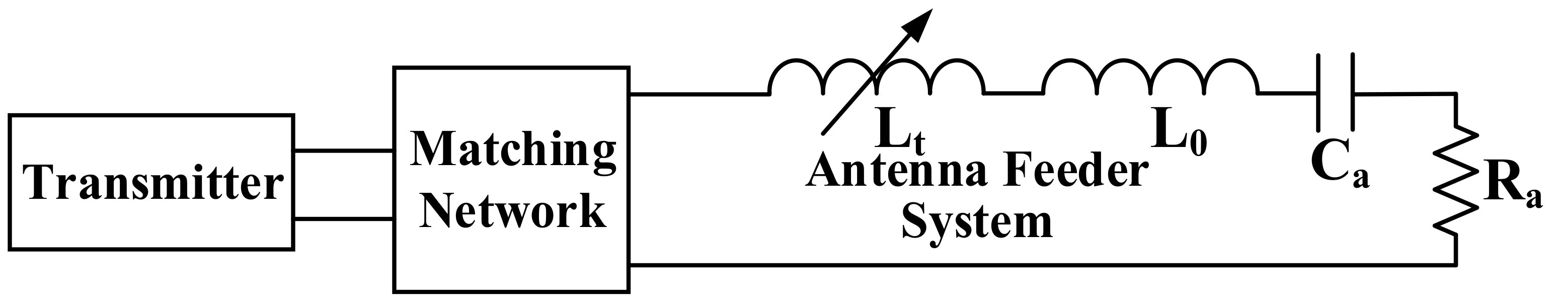
2. Fundamental Architecture of a Switching Device

As shown in Figure 1, R a represents the equivalent radiation resistance, C a represents the equivalent capacitance of the antenna, L 0 represents the fixed tuning inductor, and L t represents the variable inductor which is a coupling inductor in this paper. When the carrier frequency of the MSK signal is f h , the tuning inductance required for the antenna feeder system is L 0 and, at this time, L t = 0 . When the carrier frequency of the MSK signal is f l , the required tuning inductance for the antenna feeder system becomes L 0 + L t , L t = 1 / ( ω l 2 C a ) L 0 .
The switching device of the synchronous tuning system based on a coupling inductor, as depicted in Figure 2, primarily consists of an IGBT and a coupling inductor. The primary loop is driven by the MSK signal with the objective of achieving rapid switching of the inductor. During the IGBT turn-on state, the input impedance at the primary coil of the coupling inductor is denoted as 0. When the IGBT is turned off, the input impedance of the primary coil of the coupling inductor becomes j ω L 1 . In practical applications, precise adjustment of the number of turns in both primary and secondary coils can be achieved as n 1 = n 2 , L 1 = L 2 at this moment; however, magnetic leakage always occurs in the transformer’s air gap, leading to an inability to achieve an ideal coupling coefficient denoted as k = 1 . Moreover, internal resistance and parasitic capacitance inherent to the IGBT cannot be avoided and consequently affect the input impedance Z C I of the primary loop of the coupling inductor [21].
The value of Z C I should be equal to the impedance value of L t in Figure 1, where L t is a coupling inductor in this article. The value of Z C I will affect the resonance frequency of the antenna feeder system. In order to ensure real-time resonance of the MSK signal in the antenna feeder system, the value of Z C I needs to be adjusted in real time according to the frequency of the MSK signal, so that each frequency point corresponds to a different Z C I . The ideal scenario is when the carrier frequency of the MSK signal is f h , Z C I = 0 and the IGBT is in a conduction state when the carrier frequency of the MSK signal is f l , Z C I = j ω L 1 and the IGBT is in the cutoff state. However, due to the influence of coupling coefficient, coil resistance, IGBT internal resistance, and parasitic capacitance, the actual value of Z C I deviates from the ideal value. For example, an increase in the real part of Z C I will increase losses, while changes in the imaginary part of Z C I will affect the resonance frequency of the antenna feeder system and cause MSK signal detuning. All these factors can lead to a decrease in antenna efficiency. From Figure 1, we can obtain the formula for the antenna efficiency of this VLF transmission system [3].
η a = P a P a + P X = R a R a + ω ( L t + L 0 ) 1 ω C a = R a R a + Z C I + ω L 0 1 ω C a
In Equation (3), P a represents the radiated power, P X represents the reactive power. In order to improve antenna efficiency, we hope that the actual value of Z C I deviates as little as possible from its ideal value, and thus defines a deviation value Δ Z C I e .
Δ Z C I e = Z C I r Z C I i = R C I e + j X C I e
Z C I r represents the actual value of Z C I , Z C I i represents the ideal value of Z C I , R C I e represents the real part of Δ Z C I e , X C I e represents the imaginary part of Δ Z C I e , and it is required that R C I e n × 10 2   Ω , n × 10 3   Ω X C I e n × 10 3   Ω , n 1,9 .
In order to make the discussion clearer, in this paper, except for the IGBT and coupling inductance, all other devices are ideal devices, and this paper mainly analyzes the effects of coupling coefficient, coil resistance, IGBT internal resistance, and parasitic capacitance.

3. Performance Analysis of a Switching Device

The controlled source equivalent model of the switching device based on a coupled inductor is illustrated in Figure 3, which represents the resistances corresponding to the heat loss of the primary and secondary coils, respectively. Considering consistent coil turns and material, R 1 = R 2 . The IGBTs used in this study are of the same model, produced near each other with wafers from the same batch. A single IGBT can be represented as a resistor in parallel with a capacitor [22,23,24], where the equivalent resistor is denoted as R S W . It exhibits two states: turn-on and turn-off, with an on-resistance of R S W o n and an off-resistance of R S W o f f . Additionally, it possesses an equivalent parallel capacitance C S W , and R S W o n 1 = R S W o n 2 , R S W o f f 1 = R S W o f f 2 , C S W 1 = C S W 2 ; K represents the coupling coefficient and M denotes the mutual inductance coefficient [21].
The KCL equations for the primary and secondary loops are listed as follows.
( R 1 + j ω L 1 ) I 1 j ω M I 2 = U C I
( R 2 + 2 R S W 1 + j ω R S W C S W + j ω L 2 ) I 2 j ω M I 1 = 0
The formula is reformulated for the purpose of facilitating calculations.
Z 11 I 1 Z M I 2 = U C I
Z 22 I 2 Z M I 1 = 0
The primary loop impedance is denoted as Z 11 = R 1 + j ω L 1 , the secondary loop impedance is denoted as Z 22 = R 2 + 2 R S W 1 + j ω R S W C S W + j ω L 2 , and the mutual inductance impedance is denoted as Z M = j ω L M in Equations (3) and (4). Here, M = k L 1 L 2 . By solving the aforementioned equations, we can obtain the following results.
I 1 = Z 22 Z 11 Z 22 Z M 2 U S
I 2 = Z M Z 11 Z 22 Z M 2 U S
The input impedance of the primary loop of the coupling inductor is the following:
Z C I = U C I I 1 = Z 11 Z M 2 Z 22 = Z 11 + ω 2 M 2 Z 22
where ω 2 M 2 Z 22 is the reflected impedance, represented by Z f , and Equation (11) can be expanded to the following:
Z C I = R 1 + j ω L 1 + ω 2 M 2 ( 1 + j ω R S W C S W ) 2 R S W + ( R 2 + j ω L 2 ) ( 1 + j ω R S W C S W )
The input impedance of the primary loop of the coupled inductor is determined by Equation (12).
In practical situations such as engineering applications, it is difficult for the coupled inductor to be fully coupled, and its leakage inductance will be reflected in Z C I , resulting in excessive equivalent impedance of the coupled inductor in the antenna-fed system when the IGBT is conducting, affecting the resonance of the antenna-fed system.
For the purpose of facilitating discussion, in this section, we assume L 1 = L 2 = 15.9   μ H , f l = 19.95   k H z , f h = 20.05   k H z . When the carrier frequency of the MSK signal is f h , Z C I i = 0 , and at this time, the IGBT is in the conducting state. When the carrier frequency of the MSK signal is f l , Z C I i = j 1.993   Ω , and at this time the IGBT is in the off state. Except for IGBT and coupled inductor, all other components are ideal devices.

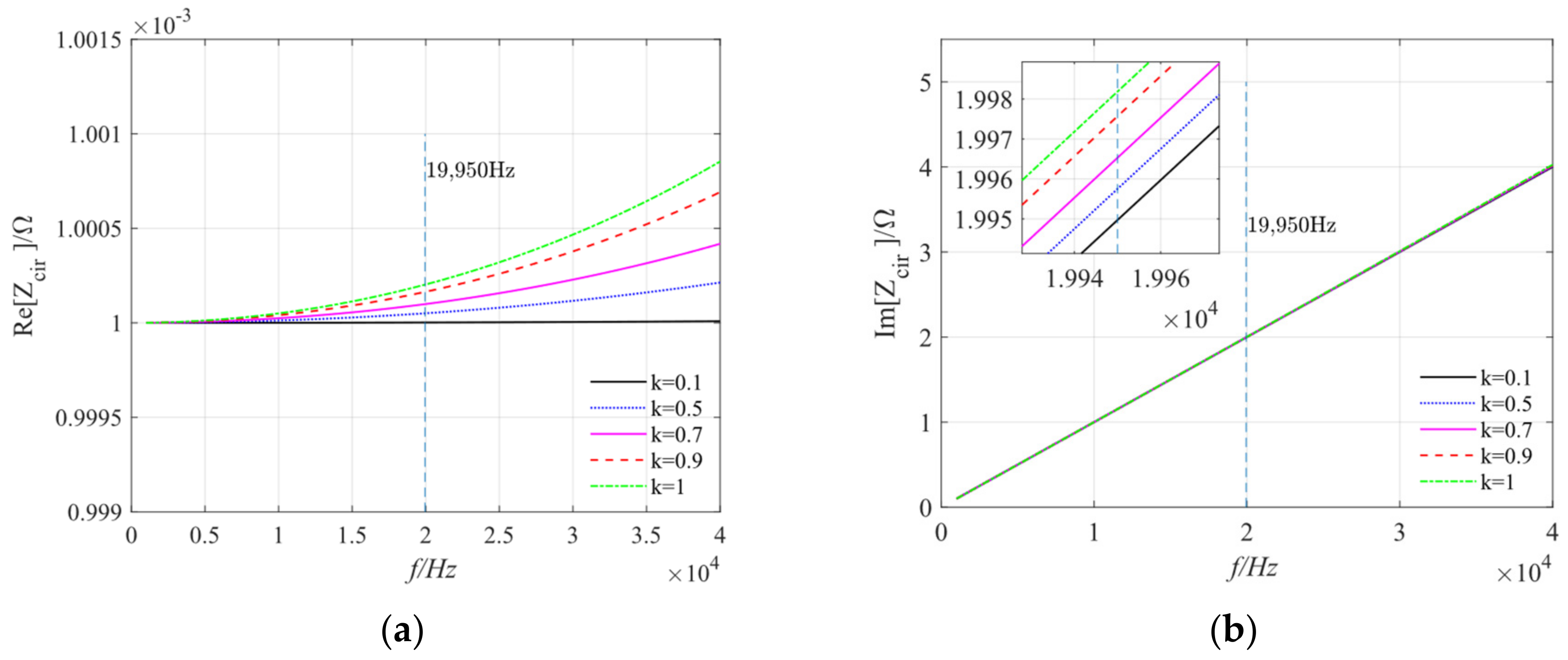
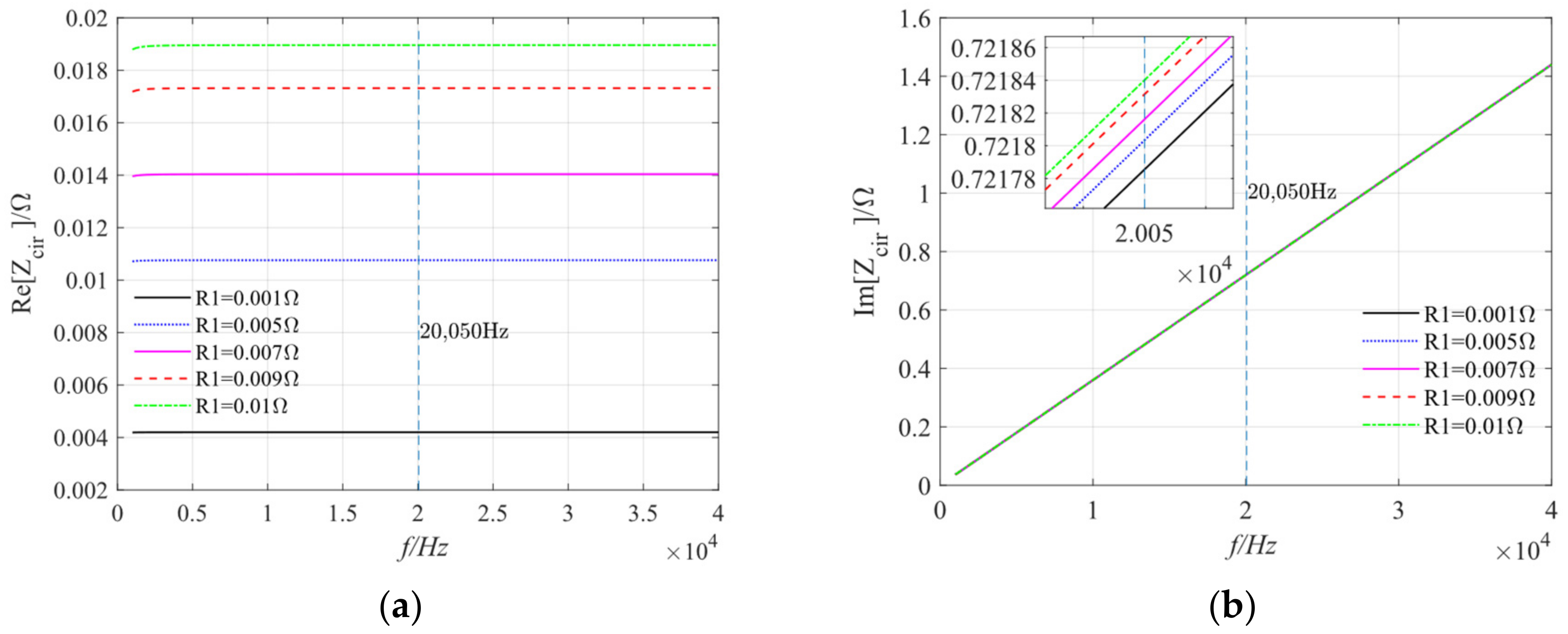
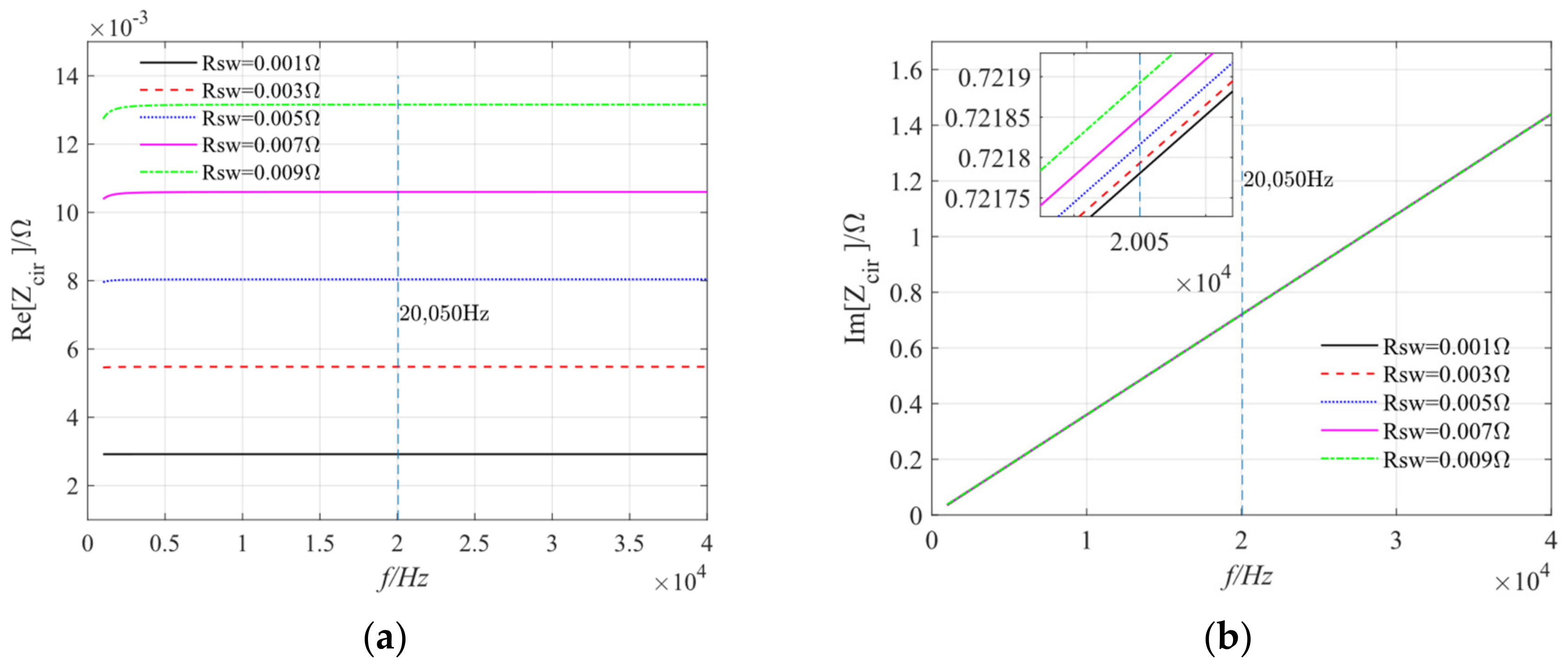
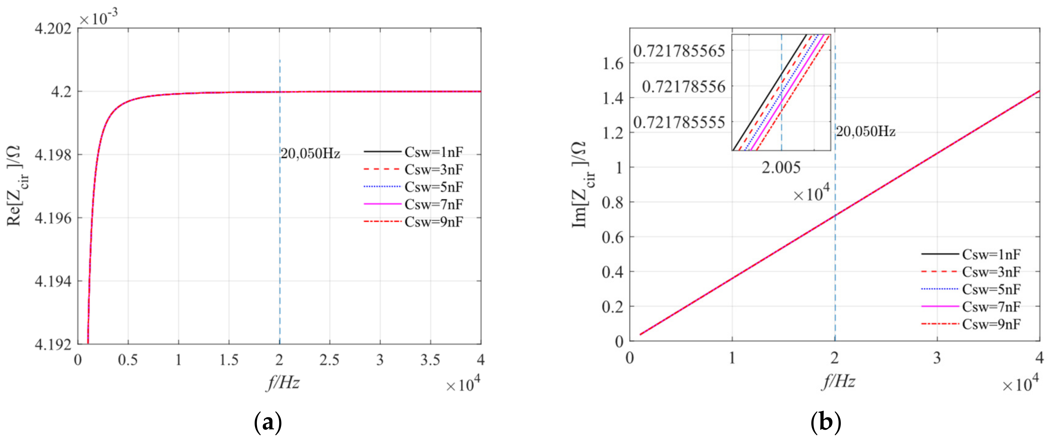
3.1. The Impact of the Coupling Coefficient and Resistance Caused by Coupling Inductance Loss

From Equation (12), we can derive the variations of Z C I r with respect to both the coupling coefficient k and frequency f , in both the IGBT turn-off state and turn-on state.
R e [ Z C I r ] is minimally influenced by k in the off state of the IGBT, as depicted in Figure 4a. The average discrepancy between curves corresponding to different values of k is approximately 2 × 10 7   Ω . From Equation (4), we can obtain that R C I e = 1 × 10 3   Ω . As depicted in Figure 4b, I m [ Z C I r ] exhibits an increasing trend with rising f during the IGBT off state, while variations in k have negligible impact. The average discrepancy between the curves corresponding to different k values is approximately 1 × 10 3   Ω . When f l = 19.95   k H z is designated as the resonant frequency, I m [ Z C I r ] = j 1.997   Ω . From Equation (4), we can obtain that X C I e = 4 × 10 3   Ω . Consequently, during the IGBT turn-off state, the coupling inductor can be equivalent to a common inductor with an inductance value of L 1 .
The impact of k on the R e [ Z C I r ] is more pronounced during the IGBT turn-on state compared to when it is turned off, as depicted in Figure 5a. However, the overall values remain below 6 × 10 3   Ω . The average discrepancy between curves corresponding to different k values is approximately 2.5 × 10 3   Ω and remains unaffected by frequency. From Equation (4), we can obtain that R C I e < 6 × 10 3   Ω . As depicted in Figure 5b, during the turn-on state of IGBT, the value of k significantly influences the I m [ Z C I r ] . As k decreases, I m [ Z C I r ] gradually increases due to the amplified leakage inductance of the coupling transformer, which is reflected in Z f and can severely impact antenna feeder system resonance.
From Equation (12), we can derive the variations of Z C I r with respect to both the coupled inductor loss resistance R 1 , R 2 and frequency f , in both the IGBT turn-off state and turn-on state.
R e [ Z C I r ] is significantly influenced by R 1 in the turn-off state of the IGBT, as depicted in Figure 6a. The average difference between curves corresponding to different values of R 1 is approximately 4 × 10 3   Ω , while it remains unaffected by frequency. From Equation (4), we can obtain that R C I e < 1 × 10 2   Ω . As depicted in Figure 6b, I m [ Z C I r ] exhibits an increasing trend with rising f during the IGBT turn-off state, while variations in R 1 have negligible impact. The average discrepancy between the curves corresponding to different k values is approximately 1 × 10 3   Ω . When f l = 19.95   k H z is designated as the resonant frequency, I m [ Z C I r ] = 1.997   Ω . From Equation (4), we can obtain that X C I e = 4 × 10 3   Ω . Consequently, during the IGBT turn-off state, the coupling inductor can be equivalent to a common inductor with an inductance value of L 1 .
R e [ Z C I r ] is significantly influenced by R 1 during the turn-on state of IGBT, as depicted in Figure 7a. The average deviation between curves corresponding to different R 1 values is approximately 7 × 10 3   Ω ; however, it remains unaffected by frequency. From Equation (4), we can obtain that R C I e < 2 × 10 2   Ω . As depicted in Figure 7b, I m [ Z C I r ] remains largely unaffected by variations in R 1 during IGBT conduction. The average discrepancy between the curves corresponding to different R 1 values is approximately 2 × 10 5   Ω . I m [ Z C I r ] escalates with an increase in f . From Equation (4), we can obtain that X C I e = 0.7   Ω , which does not meet the requirement of n × 10 3   Ω X C I e n × 10 3   Ω , n 1,9 .
In conclusion, the influence of the coupling coefficient on Z C I r can be disregarded when IGBT is in the off state. Moreover, the sizes of R 1 and R 2 are contingent upon the process of coupling inductance, and presently, the DCR value of the coupled inductor can achieve a milliohm level to fulfill the requirements outlined in this paper. In the on state of IGBT, the impact of R 1 and R 2 can be neglected; however, during this period, the coupling coefficient has a significant impact on Z C I r , and X C I e can reach 0.7   Ω .

3.2. The Impact of Internal Parameters on the Performance of IGBT

From Equation (12), we can derive the variations of Z C I r with respect to both the R S W and f , in both the IGBT turn-off state and turn-on state.
R e [ Z C I r ] in the IGBT turn-off state decreases with an increase in R S W , as depicted in Figure 8a. From Equation (4), we can determine that R C I e = 1 × 10 3   Ω . As depicted in Figure 8b, I m [ Z C I r ] exhibits an increasing trend with rising f during the IGBT turn-off state, while variations in R S W have negligible impact. The average discrepancy between curves corresponding to different R S W values is approximately 1 × 10 12   Ω . When f l = 19.95   k H z is designated as the resonant frequency, I m [ Z C I r ] = 1.995   Ω . From Equation (4), we can obtain that X C I e = 2 × 10 3   Ω . Consequently, during the IGBT turn-off state, the coupling inductor can be equivalent to a common inductor with an inductance value of L 1 .
R e [ Z C I r ] increases with the increase in R S W when IGBT is in the turn-on state, as depicted in Figure 9a, yet it consistently remains below 1 × 10 2   Ω . The average deviation between curves corresponding to different values of R S W is approximately 5 × 10 3   Ω , and this discrepancy shows no significant dependence on frequency. From Equation (4), we can obtain that R C I e < 13 × 10 3   Ω . As depicted in Figure 9b, I m [ Z C I r ] remains largely unaffected by variations in R S W during the IGBT turn-on state. The average discrepancy between the curves corresponding to different R S W values is approximately 7 × 10 5   Ω . The imaginary component of Z C I escalates with an increase in f . From Equation (4), we can obtain that X C I e = 0.7   Ω , which does not meet the requirement of n × 10 3   Ω X C I e n × 10 3   Ω , n 1,9 .
R e [ Z C I r ] in the IGBT turn-off state is minimally influenced by C S W , as depicted in Figure 10a, with an overall value of approximately 1 × 10 3   Ω . Notably, there exists an average deviation of around 1 × 10 8   Ω between curves corresponding to different values of C S W . From Equation (4), we can obtain that R C I e = 1 × 10 3   Ω . As depicted in Figure 10b, I m [ Z C I r ] exhibits an increasing trend with rising f during the IGBT turn-off state, while variations in C S W have negligible impact. The average discrepancy between the curves corresponding to different C S W values is approximately 6 × 10 4   Ω . When f l = 19.95   k H z is designated as the resonant frequency, I m [ Z C I r ] = 1.995   Ω . From Equation (4), we can obtain that X C I e = 2 × 10 3   Ω . Consequently, during the IGBT turn-off state, the coupling inductor can be equivalent to a common inductor with an inductance value of L 1 .
As depicted in Figure 11a, during the turn-on state of IGBT, the impact of C S W on the R e [ Z C I r ] is negligible. The overall R e [ Z C I r ] approximately equal to 4 × 10 3   Ω , with an average deviation of approximately 1 × 10 11   Ω among curves corresponding to different values of C S W . Furthermore, as the frequency surpasses a certain threshold, the curves tend to exhibit a more flattened profile. From Equation (4), we can obtain that R C I e = 4 × 10 3   Ω . As depicted in Figure 11b, I m [ Z C I r ] remains largely unaffected by variations in C S W during IGBT turn-on. The average discrepancy between the curves corresponding to different C S W values is approximately 3 × 10 9   Ω . I m [ Z C I r ] escalates with an increase in f . From Equation (4), we can obtain that X C I e = 0.7   Ω , which does not meet the requirement of n × 10 3   Ω X C I e n × 10 3   Ω , n 1,9 .
In conclusion, the influence of internal parameters of IGBT on Z C I r can be disregarded when the IGBT is in the turn-off state. When the IGBT is in the turn-on state, R S W has a more significant impact on the R e [ Z C I r ] , while C S W s’ effect on Z C I r can be neglected. However, X C I e can still reach 0.7   Ω , which is mainly influenced by the coupling coefficient.
Based on the analysis presented in this section, it can be inferred that the coupling coefficient and internal parameters of IGBT do not significantly affect Z C I r when IGBT is in the turn-off state. However, when IGBT is in the turn-on state, k becomes the primary factor influencing Z C I r , while R S W mainly impacts its real part resulting in thermal losses.

4. Adaptive Input Impedance Optimization Algorithm Based on Variable Capacitor (VC-ADIO)

To optimize the value of Z C I under IGBT turn-on state and meet the performance requirements of the switching device in this paper, we propose an adaptive input impedance optimization algorithm based on a variable capacitor (VC-ADIO).

4.1. Calculation Method for Variable Capacitor C t

Before proposing the algorithm, it is imperative to thoroughly analyze the calculation methodology of variable capacitor C t , which serves as the fundamental element in this algorithm, and extensively discuss its impact on Z C I . Figure 12 illustrates the controlled source equivalent model of a switch device based on a variable capacitor.
The input impedance of the primary loop for this model can be obtained by applying the calculation method described in Equations (5)–(12).
Z C I = R 1 + j ω L 1 + ω 2 M 2 R 2 + 2 R S W 1 + j ω R S W C S W + j ω L 2 + 1 j ω C t
1 j ω C t = ω 2 M 2 Z C I R 1 j ω L 1 R 2 2 R S W 1 + j ω R S W C S W j ω L 2
The variation of Z C I r with respect to both C t and f can be derived from Equation (13).
R e [ Z C I r ] is minimally influenced by C t in the turn-off state of the IGBT, as depicted in Figure 13a. The average discrepancy between curves corresponding to different values of C t is approximately 1 × 10 8   Ω . Although the R e [ Z C I r ] increases with an increasing f , it maintains a magnitude around 10 3   Ω overall. From Equation (4), we can obtain that R C I e = 1 × 10 3   Ω . As depicted in Figure 13b, the imaginary component of Z C I exhibits an increasing trend with rising f during the IGBT off state, while variations in C t have negligible impact. The average discrepancy between the curves corresponding to different C t values are approximately 1 × 10 5   Ω . When f l = 19.95   k H z is designated as the resonant frequency, I m [ Z C I r ] = 1.997   Ω . From Equation (4), we can obtain that X C I e = 0 . Consequently, during the IGBT turn-off state, the coupling inductor can be equivalent to a common inductor with an inductance value of L 1 .
As depicted in Figure 14a, during the turn-on state of IGBT, R e [ Z C I r ] is around 1 × 10 3   Ω at the required frequency, although it will have a mutation at a certain frequency on the premise that C t satisfies Equation (14). In Figure 14b, under the turn-on state of IGBT and satisfying Equation (14), although there are abrupt variations in the I m [ Z C I r ] at certain frequencies, it remains approximately 3 × 10 5   Ω at the desired resonant frequency f h = 20.05   k H z . From Equation (4), we can determine that X C I e = 3 × 10 5   Ω , which meets the requirement of n × 10 3   Ω X C I e n × 10 3   Ω , n 1,9 .
In conclusion, during the IGBT turn-off state, the impact of C t on Z C I r is negligible and can be disregarded. However, in the IGBT turn-on state, C t significantly influences the Z f of the coupled inductor and ultimately manifests itself in Z C I r s’ value. Therefore, it is crucial to focus on accurately calculating C t s’ value during the turn-on state of IGBT.

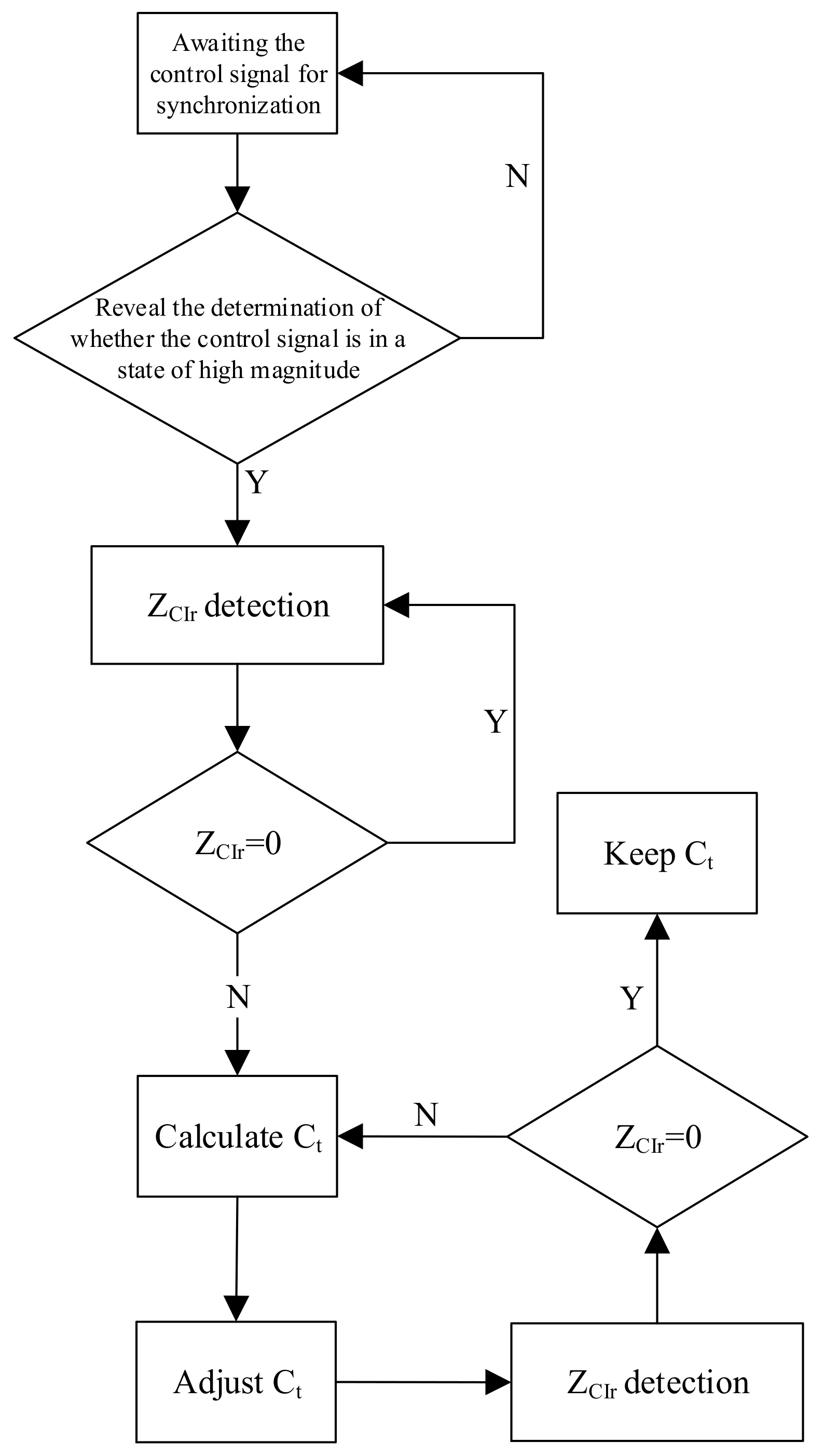
4.2. Basic Process of Adaptive Input Impedance Optimization Algorithm Based on Variable Capacitor

The primary objective of optimizing the VC-ADIO is to achieve stability of the coupling inductance Z C I r around 0 during the IGBT turn-on state. Notably, this article does not delve into the specific design and manufacturing aspects of variable capacitors, as there are already well-established solutions available [25,26,27]. The specific process is as follows.
The frequency switching of the control signal is synchronized with the MSK signal, as illustrated in Figure 15. During periods when the control signal is high, it performs Z C I r detection on the primary circuit of the coupled inductor. If Z C I r = 0 or satisfies the requirement that R C I e n × 10 2   Ω , n × 10 3   Ω X C I e n × 10 3   Ω , n 1,9 , continue with the detection process; otherwise, calculate and adjust the value of C t to optimize input impedance and repeat the Z C I r detection procedure. If Z C I r = 0 or meets the requirement that R C I e n × 10 2   Ω , n × 10 3   Ω X C I e n × 10 3   Ω , n 1,9 , retain the current value of C t ; otherwise, recalculate until all requirement is met.
When the control signal transitions to a low level, C t maintains its current value. Upon the control signal transitioning back to a high level, C t retains its current value and subsequently determines whether an adjustment is necessary following Z C I r detection.
The literature [28] proposes a design method for customized fixture adapters. Through a systematic parasitic de-embedding process, the parasitic effects introduced by adding additional connectors to the adapter are resolved. Improve the accuracy of measuring choke coil impedance. This paper mainly focuses on the feasibility of the whole synchronous tuning system and the optimization method. The design of a system involves many factors. Therefore, in order to make the discussion clearer, we consider that the results of impedance measurement are accurate.

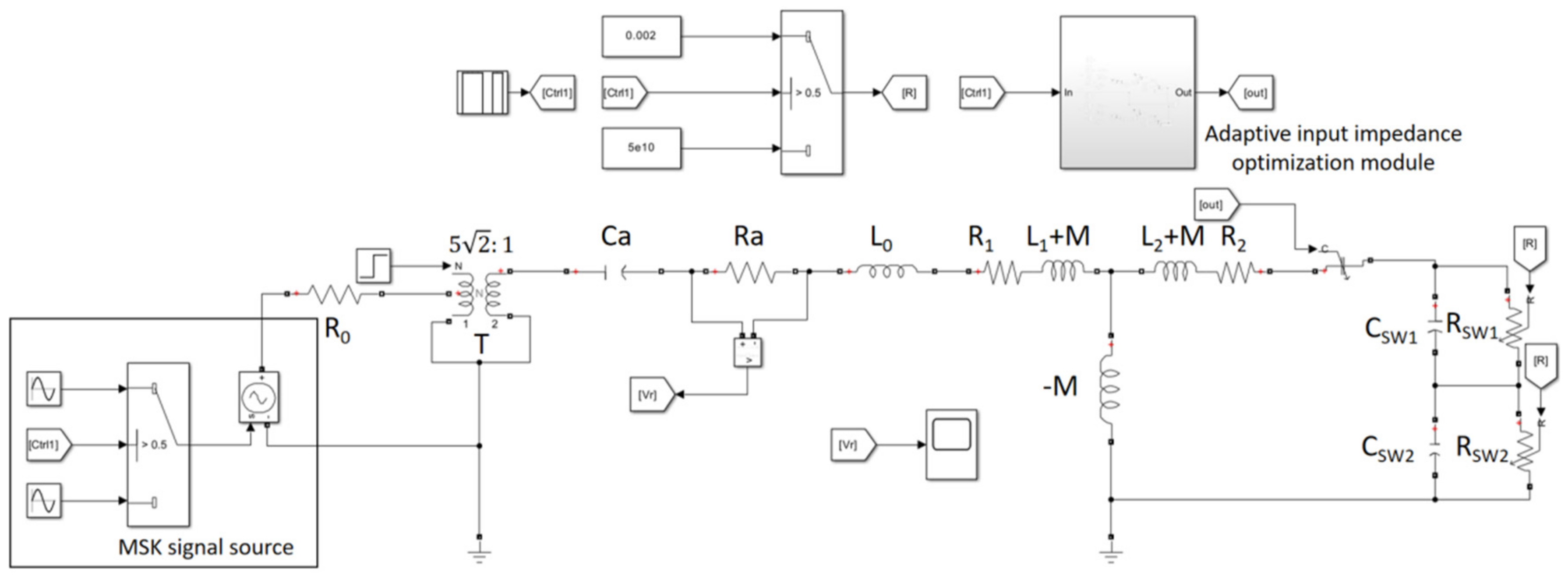
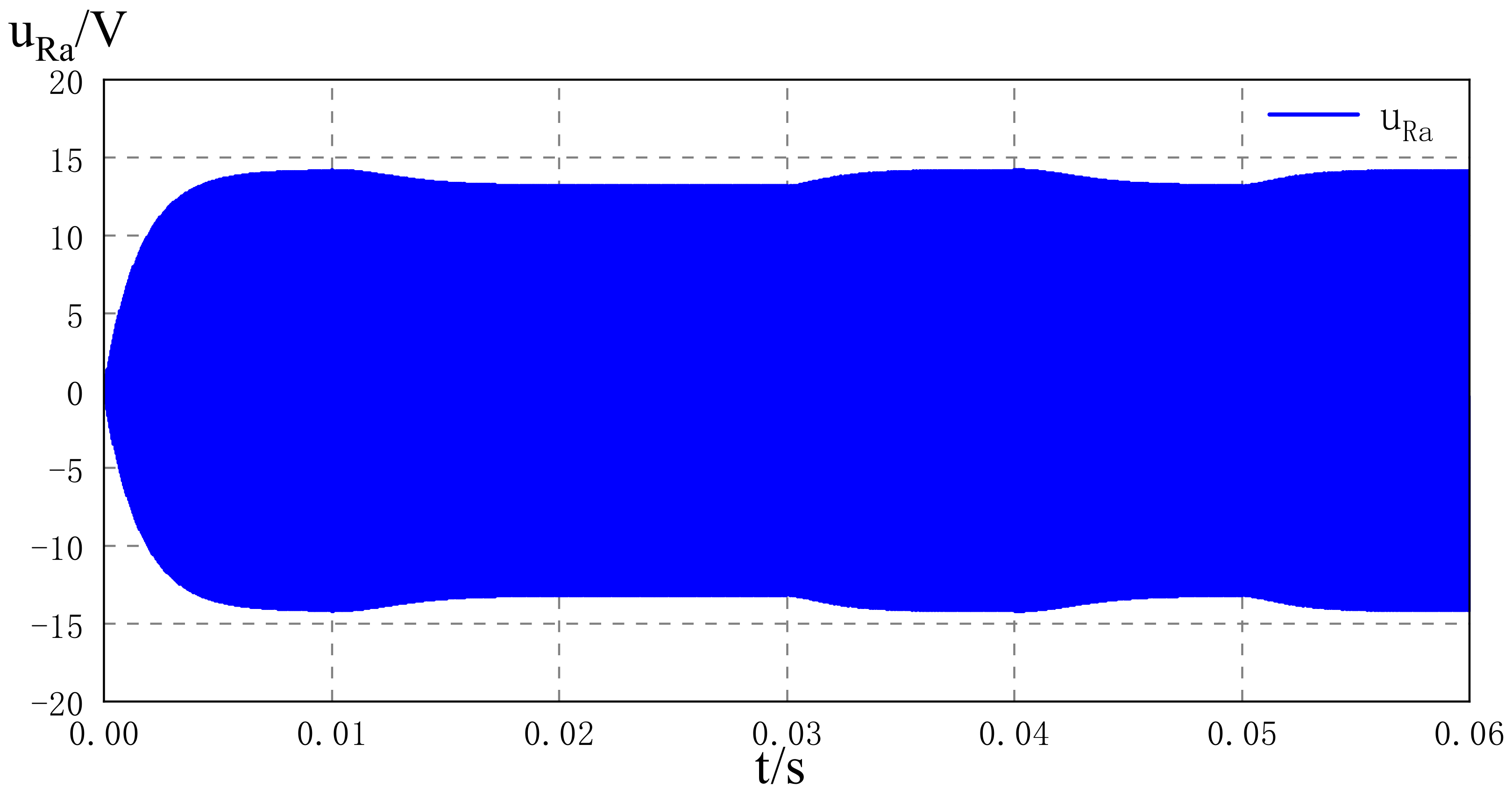
5. Simulation and Experiment

In order to validate the efficacy of the VC-ADIO, this section establishes the model for a VLF transmission system based on a coupled inductor decoupling equivalent circuit [29,30].
As depicted in Figure 16, a single IGBT can be represented as a resistor in parallel with a capacitor, R S W o n = 0.002   Ω , R S W o f f = 5   M Ω , k = 0.8 , L 1 = L 2 = 15.9   μ H , R 1 = R 2 = 0.001   Ω , L 0 = 1.58   m H , f l = 19.95   k H z , f h = 20.05   k H z , C a is the equivalent capacitance of the antenna, C a = 39.79   n F , R a is the equivalent radiation resistance of the antenna, R a = 1   Ω , symbol rate is 200 B, control signal is [0 0 1 1 1 1 0 0 1 1 0 0], R 0 is signal source internal resistance, and R 0 = 50   Ω . The turns ratio of ideal transformer T is 5 2 : 1 .
The simulation results are presented in the subsequent figures. The average power can be calculated from the time-domain waveform as follows.
P ¯ = 1 T T 2 T 2 u ( t ) i ( t ) d t
As depicted in Figure 17, after impedance optimization, the antenna feeder system resonates in real time, so the voltage waveform at both ends of R a is a constant envelope, and the voltage is stable at 14.13 V. The average power is approximately 98.73 W. As depicted in Figure 18, before impedance optimization, obvious resonance occurs in the antenna feeder system, so the voltage waveform at both ends of R a is no longer a constant envelope, and the voltage drops to 13 V. The average power is approximately 92.26 W. This discrepancy primarily arises from an excessively large imaginary part of Z C I r . Consequently, it causes a deviation in the resonance point of the antenna feeder system and amplifies reactive power consumption within the system.
As shown in Figure 19, the experimental setup is mainly composed of a signal source, a switching device of the synchronous tuning system, an equivalent antenna, a coupling inductor, and a fixed inductor, and the specific parameters are shown in the simulation model. The control signal is [0 1 0 1 0 1 0 1 0 1]. The test results are as follows.
As depicted in Figure 20, after impedance optimization, the antenna feeder system resonates in real time, so the voltage waveform at both ends of R a is a constant envelope, and the voltage is stable at 14.3 V. The average power is approximately 102.25 W. As depicted in Figure 21, before impedance optimization, obvious resonance occurs in the antenna feeder system, so the voltage waveform at both ends of R a is no longer a constant envelope, and the voltage drops to 12.5 V. The average power is approximately 90.19 W. The experimental results are close to the simulation results.
The simulation and experimental results indicate that the utilization of the VC-ADIO algorithm can significantly enhance the performance of switch devices, leading to an increased radiation power of VLF antennas. This is mainly because, through synchronous switching of switches and impedance optimization, the reactance component in the input impedance of the antenna feeder system approaches zero, thereby keeping the antenna feeder system always tuned to the carrier frequency of the MSK signal and greatly reducing reactive power.

6. Conclusions

This article presents an analysis of the switch device’s performance in a synchronous tuning system, highlighting the coupling coefficient and IGBT turn-on resistance as the primary factors influencing its performance. It proposes an adaptive input impedance optimization algorithm based on variable capacitance to enhance the input impedance of the coupled inductor primary circuit. The radiated power of the VLF antenna is improved effectively.

Author Contributions

Conceptualization, S.W.; Methodology, S.W.; Software, H.Z.; Validation, S.W.; Writing—original draft, S.W.; Writing—review & editing, X.X.; Supervision, X.X. All authors have read and agreed to the published version of the manuscript.

Funding

This research was funded by Basic Strengthening Program Technological Field Fund, grant number 2021-JCJQ-JJ-0749.

Data Availability Statement

Data are contained within the article.

Conflicts of Interest

The authors declare no conflict of interest.

References

  1. Wen, W.F. Research on Miniaturized HF Ultra-HF Wideband Antenna and Matching Network. Master’s Thesis, University of Electronic Science and Technology, Chengdu, China, 25 August 2024. [Google Scholar]
  2. Dan, D. Research on Wideband and Miniaturization of Low-Frequency Antenna. Master’s Thesis, University of Electronic Science and Technology, Chengdu, China, 2014. [Google Scholar]
  3. Liu, C.; Jiang, H.; Huang, J.H. Very Low Frequency Communication; Haichao Publishing House: Beijing, China, 2008; p. 122. [Google Scholar]
  4. Fan, C.; Cao, L. Communication Principle; National Defense Industry Press: Beijing, China, 2006; p. 242. [Google Scholar]
  5. Watt, A.D. VLF Radio Engineering; Pergamon: Bergama, Turkey, 1967. [Google Scholar]
  6. Wolff, H. High-Speed Frequency-Shift Keying of LF and VLF Radio Circuits. Ire Trans. Commun. Syst. 1957, 5, 29–42. [Google Scholar] [CrossRef]
  7. Dong, Y.; Jiang, Y.; Zhang, J. VLF emission system based on MSK spectrum frequency characteristic study. J. Radio Sci. J. 2010, 3, 6. [Google Scholar]
  8. Simpson, T.; Roberts, M.; Berg, E. Developing a broadband circuit model for the Cutler VLF antenna. In Proceedings of the Antennas & Propagation Society International Symposium, Boston, MA, USA, 8–13 July 2001. [Google Scholar] [CrossRef]
  9. Berg, E.C.; Roberts, M.A.; Simpson, T.L. Dual-frequency distortion predictions for the Cutler VLF array. Aerosp. Electron. Syst. IEEE Trans. 2003, 39, 1016–1034. [Google Scholar] [CrossRef]
  10. Zhang, W.; Zheng, L.; Dong, Y. Very low frequency transmitting antenna dynamic tuning bandwidth study. J. Ship Electr. Eng. 2009, 10, 4. [Google Scholar] [CrossRef]
  11. Dong, Y.; Liu, C. Dynamic tuning VLF antenna performance. J. Nav. Eng. Univ. 2010, 22, 98–102. [Google Scholar]
  12. Jin, G.; Dong, Y. VLF emission system synchronous tuning study. J. Mod. Electron. Technol. 2011, 34, 3. [Google Scholar]
  13. Jin, G.; Dong, Y. MSK synchronization based on FPGA tuning study. Microcomput. Inf. 2012, 3, 2. [Google Scholar]
  14. Ling, J.; Dong, Y.; Xu, H. Very low frequency transmitting system performance simulation. J. Radio Commun. Technol. 2015, 5, 74–76. [Google Scholar] [CrossRef]
  15. Johannessen, P.R. Automatic Tuning of High-Q Antenna For VLF FSK Transmission. IEEE Trans. Commun. Syst. 1964, 12, 110–115. [Google Scholar] [CrossRef]
  16. Hartley, H. Electronic Broad Banding of VLF/LF Antennas for FSK Radio Communication. IEEE Trans. Commun. Technol. 1971, 19, 555–561. [Google Scholar] [CrossRef]
  17. Firman, C.M. Synchronized Turn-Off of VLF Antennae: US19720222194. U.S. Patent 3904966A, 18 June 2024. [Google Scholar]
  18. Johannessen, P.R.; Planckp, V. Antenna Tuning System and Method. U.S. Patent 4689803, 1 September 1987. [Google Scholar]
  19. Johnson, L.J. Magnetic Amplifier Switchfor AutomaticTuning of VIF Transmitting Antenna. U.S. Patent 5034697, 23 July 1991. [Google Scholar]
  20. Ivan, W.; Ivan, W.; Guy, B. Switchable Inductor for Strong Currents and Antenna Tuning Circuit Provided with at Least One Such Inductance: FR19920005722. U.S. Patent FR2691308A1, 5 May 2024. [Google Scholar]
  21. Zu, Y.; Li, W.; Lv, Y. Fundamentals of Circuit Analysis, 2nd ed.; Publishing House of Electronics Industry: Beijing, China, 2014. [Google Scholar]
  22. Volke, A.; Hornkamp, M. IGBT Modules: Technology, Drivers and Applications; Infineon Technologies AG: Munich, Germany, 2012. [Google Scholar]
  23. Khanna, V.K. Insulated Gate Bipolar Transistor IGBT Theory and Design; Wiley-IEEE Press: Hoboken, NJ, USA, 2003. [Google Scholar] [CrossRef]
  24. Mao, H.-K.; Wang, Y.; Wu, X.; Su, F.-W. Simulation Study of 4H-SiC Trench Insulated Gate Bipolar Transistor with Low Turn-Off Loss. Micromachines 2019, 10, 815. [Google Scholar] [CrossRef] [PubMed]
  25. Deng, J.; Li, H.; Ruan, Q. A Differential Complementary Variable Capacitor for VCO. U.S. Patent CN117277968A, 22 December 2023. [Google Scholar]
  26. Zhang, D.; Hong, J. A Vacuum Capacitor that Can Change the Capacity of the Capacitor. U.S. Patent CN215955107U, 4 March 2022. [Google Scholar]
  27. Jin, P.; Li, Z.; Guo, Y. An Online Debugging Method for Automatic Resonance Regulation of a Variable-Capacitance Bidirectional CLLC Resonant Converter. U.S. Patent CN117375425A, 9 January 2024. [Google Scholar]
  28. Jie, H.; Gao, S.-P.; Zhao, Z.; Fan, F.; Sasongko, F.; Gupta, A.K.; See, K.Y. VNA-Based Fixture Adapters for Wideband Accurate Impedance Extraction of Single-Phase EMI Filtering Chokes. IEEE Trans. Ind. Electron. 2023, 70, 7821–7831. [Google Scholar] [CrossRef]
  29. Alonso, J.M.; Martinez, G.; Perdigao, M.; do Prado, R.N. A Systematic Approach to Modeling Complex Magnetic Devices Using SPICE: Application to Variable Inductors. IEEE Trans. Power Electron. 2016, 31, 7735–7746. [Google Scholar] [CrossRef]
  30. Perdigao, M.S.; Alonso, J.M.; Costa, M.A.D.; Saraiva, E. A variable inductor MATLAB/Simulink behavioral model for application in magnetically-controlled electronic ballasts. In Proceedings of the International Symposium on Power Electronics, Ischia, Italy, 11–13 June 2008. [Google Scholar] [CrossRef]
Figure 1. Equivalent circuit diagram of a very low-frequency transmission system using synchronous tuning technology (ignoring loss resistance) [7].
Electronics 13 03457 g001
Figure 2. The fundamental architecture of the switching device of the synchronous tuning system based on coupled inductor.
Electronics 13 03457 g002
Figure 3. The controlled source equivalent model of the switching device based on coupled inductor.
Electronics 13 03457 g003
Figure 4. The variation of Z C I r with k and f in the IGBT turn-off state. (a) The variation of the R e [ Z C I r ] with k and f ; (b) the variation of the I m [ Z C I r ] with k and f .
Electronics 13 03457 g004
Figure 5. The variation of Z C I r with k and f in the IGBT turn-on state. (a) The variation of the R e [ Z C I r ] with k and f; (b) the variation of the imaginary part of I m [ Z C I r ] with k and f.
Electronics 13 03457 g005
Figure 6. The variation of Z C I r with R 1 and f in the IGBT turn-off state. (a) The variation of the R e [ Z C I r ] with R 1 and f; (b) the variation of the I m [ Z C I r ] with R 1 and f.
Electronics 13 03457 g006
Figure 7. The variation of Z C I r with R 1 and f in the IGBT turn-on state. (a) The variation of the real part of R e [ Z C I r ] with R 1 and f; (b) the variation of the I m [ Z C I r ] with R 1 and f.
Electronics 13 03457 g007
Figure 8. The variation of Z C I r with R S W and f in the IGBT turn-off state. (a) The variation of the R e [ Z C I r ] with R S W and f; (b) the variation of the I m [ Z C I r ] with R S W and f.
Electronics 13 03457 g008
Figure 9. The variation of Z C I r with R S W and f in the IGBT turn-on state. (a) The variation of the R e [ Z C I r ] with R S W and f; (b) the variation of the I m [ Z C I r ] with R S W and f.
Electronics 13 03457 g009
Figure 10. The variation of Z C I r with C S W and f in the IGBT turn-off state. (a) The variation of the R e [ Z C I r ] with C S W and f; (b) the variation of the I m [ Z C I r ] with C S W and f.
Electronics 13 03457 g010
Figure 11. The variation of Z C I r with C S W and f in the IGBT turn-on state. (a) The variation of the R e [ Z C I r ] with C S W and f; (b) the variation of the I m [ Z C I r ] with C S W and f.
Electronics 13 03457 g011
Figure 12. The controlled source equivalent model of a switch device based on variable capacitor.
Electronics 13 03457 g012
Figure 13. The variation of Z C I r with C t and f in the IGBT turn-off state. (a) The variation of the R e [ Z C I r ] with C t and f; (b) the variation of the I m [ Z C I r ] with C t and f.
Electronics 13 03457 g013
Figure 14. The variation of Z C I r with C t and f in the IGBT turn-on state. (a) The variation of the R e [ Z C I r ] with C t and f; (b) the variation of the I m [ Z C I r ] with C t and f.
Electronics 13 03457 g014
Figure 15. Flowchart of adaptive input impedance optimization algorithm based on variable capacitor.
Electronics 13 03457 g015
Figure 16. The model for a VLF transmission system based on a coupled inductor decoupling equivalent circuit.
Electronics 13 03457 g016
Figure 17. The voltage across R a after impedance optimization.
Electronics 13 03457 g017
Figure 18. The voltage across R a before impedance optimization.
Electronics 13 03457 g018
Figure 19. Schematic diagram of the experimental setup.
Electronics 13 03457 g019
Figure 20. The voltage across R a after impedance optimization.
Electronics 13 03457 g020
Figure 21. The voltage across R a before impedance optimization.
Electronics 13 03457 g021
Disclaimer/Publisher’s Note: The statements, opinions and data contained in all publications are solely those of the individual author(s) and contributor(s) and not of MDPI and/or the editor(s). MDPI and/or the editor(s) disclaim responsibility for any injury to people or property resulting from any ideas, methods, instructions or products referred to in the content.

