Article

A Self-Biased Triggered Dual-Direction Silicon-Controlled Rectifier Device for Low Supply Voltage Application-Specific Integrated Circuit Electrostatic Discharge Protection

1
Beijing Smartchip Microelectronics Technology Company Limited, Beijing 100192, China
2
College of Physics and Information Engineering, Fuzhou University, Fuzhou 350108, China
*
Author to whom correspondence should be addressed.
Electronics 2024, 13(17), 3458; https://doi.org/10.3390/electronics13173458
Submission received: 2 August 2024 / Revised: 25 August 2024 / Accepted: 29 August 2024 / Published: 30 August 2024

Abstract

:
A direct bidirectional current discharge path between the input/output (I/O) and ground (GND) is essential for the robust protection of charging device models (CDM) in the tightly constrained design parameters of advanced low-voltage (LV) processes. Dual-direction silicon controlled rectifiers (DDSCRs) serve as ESD protection devices with high efficiency unit area discharge, enabling bidirectional electrostatic protection. However, the high trigger voltage of conventional DDSCR makes it unsuitable for ASICs used for the preamplification of biomedical signals, which only operate at low supply voltage. To address this issue, a self-biased triggered DDSCR (STDDSCR) structure is proposed to further reduce the trigger voltage. When the ESD pulse comes, the external RC trigger circuit controls the PMOS turn-on by self-bias, and the current release path is opened in advance to reduce the trigger voltage. As the ESD pulse voltage increases, the SCR loop opens to establish positive feedback and drain the amplified current. Additionally, the junction capacitance is decreased through high-resistance epitaxy and low-concentration P-well injection to further lower the trigger voltage. The simulation results of LTspice and TCAD respectively demonstrate that ESD devices can clamp transient high voltages earlier, with low parasitic capacitance and leakage current suitable for ESD protection of high-speed ports up to 1.5 V under normal operating conditions.

1. Introduction

Given the high susceptibility of integrated circuits fabricated through the CMOS process to electrostatic discharge (ESD), it is imperative to implement effective ESD protection strategies. This need is particularly urgent for high-speed I/O interface circuits [1]. Hence, we have to constantly explore and enhance ESD protection design to guarantee the safety and reliability of high-speed integrated circuits. SCR devices are employed as effective ESD protection devices due to their high robustness, compact layout area, small on-resistance, low parasitic capacitance, low leakage current, and absence of latching in low-voltage environments [2,3]. In the low-voltage CMOS process, the traditional SCR device consists of P+, N well, P well and N+. The equivalent circuit of SCR is composed of PNP BJT (QPNP) and NPN BJT (QNPN). When a positive ESD pulse occurs at the anode of the device, it opens up and forms internal triode conduction that creates a positive feedback loop for discharging the large current from ESD. However, due to their slow on–off speeds [4], SCR protection devices often fail when exposed to fast transient pulses similar to those found in charging device models (CDM), leading to damage in core circuits caused by large overshoot voltages. Previous works have proposed several solutions aimed at reducing trigger voltage in order to improve on–off speed. For instance, inductor-assisted SCR devices designed for high-frequency applications trigger at 5 V [5], but this requires additional inductor area. Grid-bound SCR devices utilize pseudo-grids to reduce the distance between anode and cathode, but necessitate extra process steps such as blocking silicides or forming Schottky junctions in order to decrease the leakage current or increase the holding voltage. An improved SCR called the direct-connected SCR (DCSCR) [6] can achieve very low trigger voltages (~1.5 V) and low parasitic capacitance, but there are bidirectional voltage protection and sufficient voltage blocking problems that need to be solved. To protect I/O ports with operating voltage ranges between negative and positive, the bidirectional SCR (DDSCR) is capable of bidirectional voltage blocking with its compact layout topology [7,8]. Compared with SCR, DDSCR has one less PN junction reduced-capacitance diode on the on-path to obtain a lower clamping voltage. However, since biomedical signal pre-amplification ASICs can typically operate at low supply voltages, the trigger voltage of DDSCR needs to be improved to narrow the ESD design window. To optimize the trigger voltage of DDSCR, an LTDDSCR has been proposed previously [9,10]. It adopts a P-type trigger junction across the two trap regions to reduce the trigger voltage, which can reduce the trigger voltage to about 10 V for ESD protection applications of 5 V. To further reduce the trigger voltage, a self-biased trigger DDSC (STDDSCR) is proposed by using a self-biased RC trigger facilitating the circuit and taking advantage of the low capacitance of DDSCR without using a reduced capacitance diode.

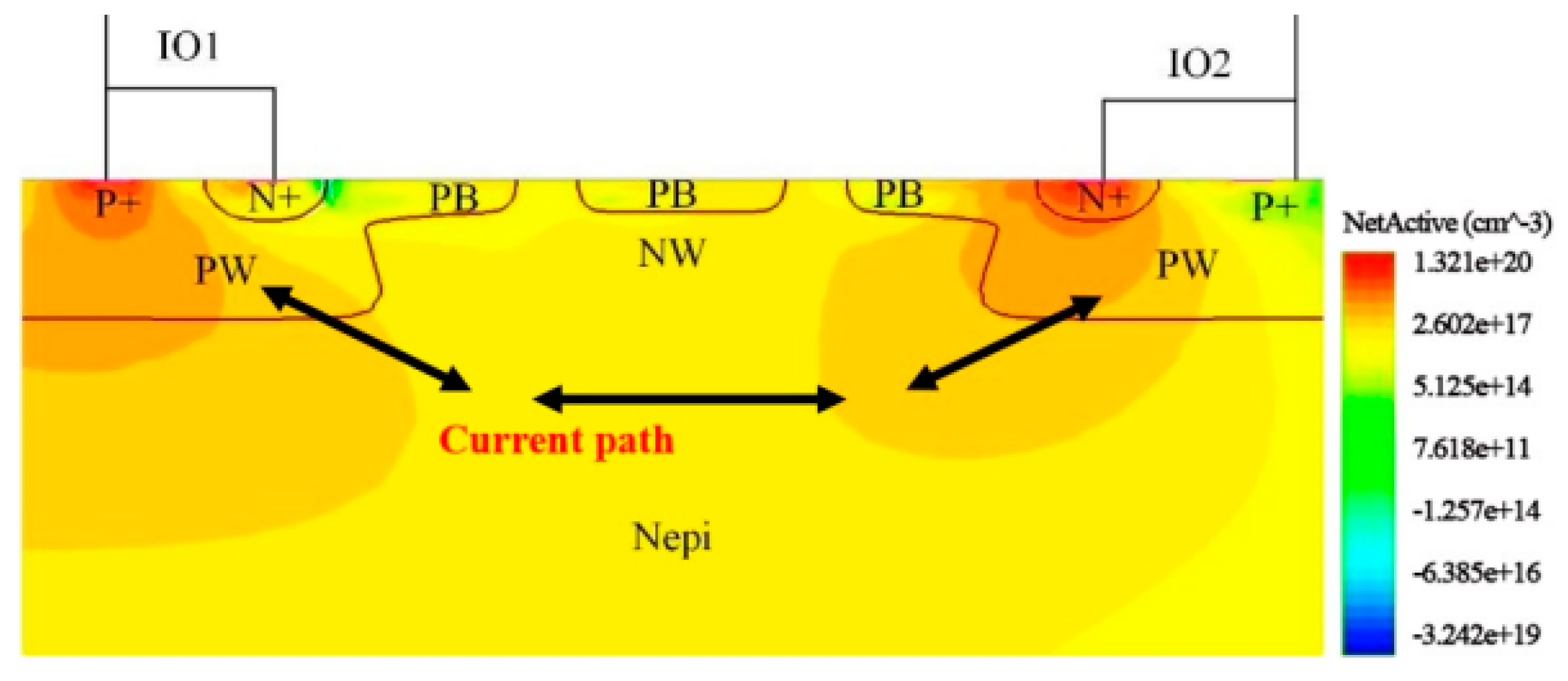
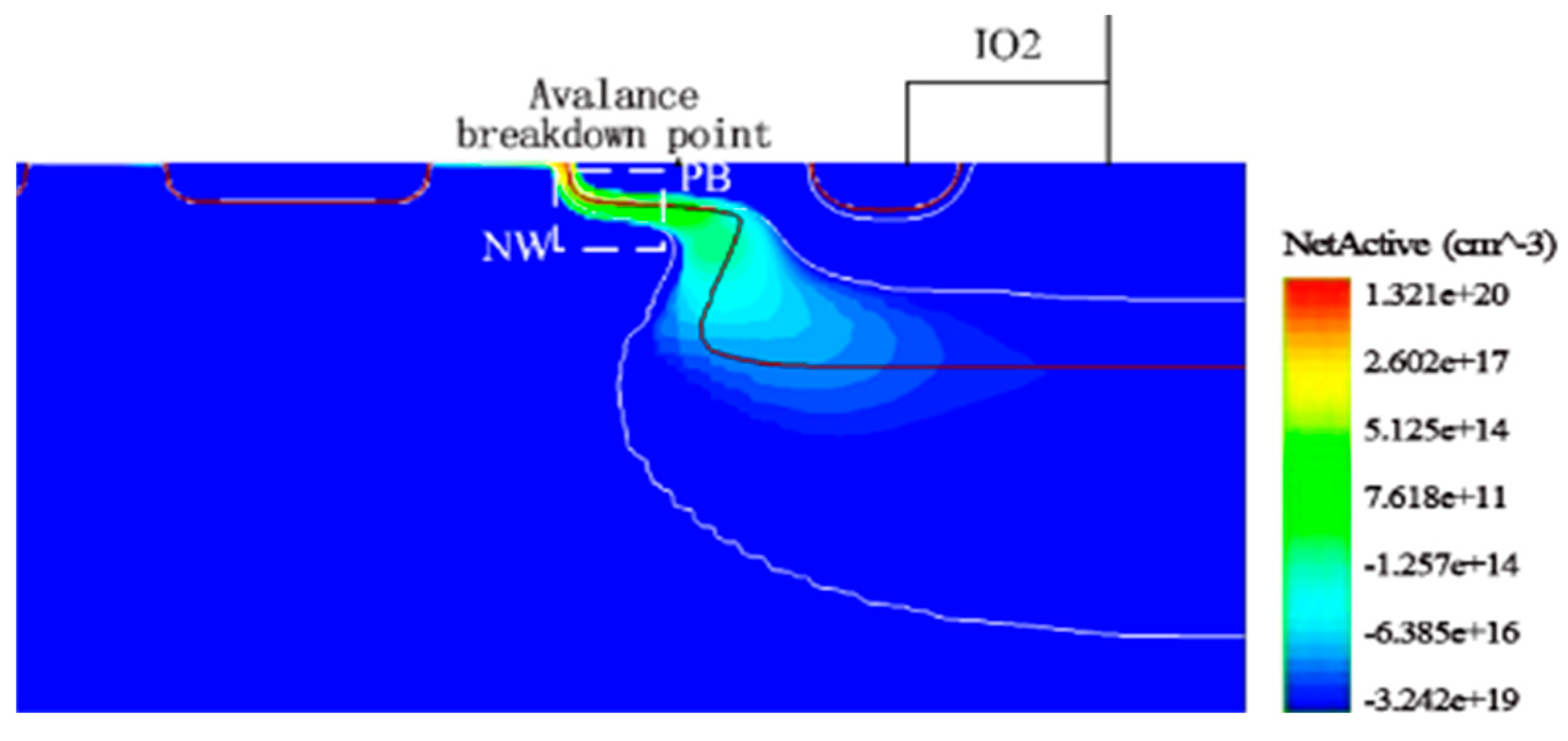
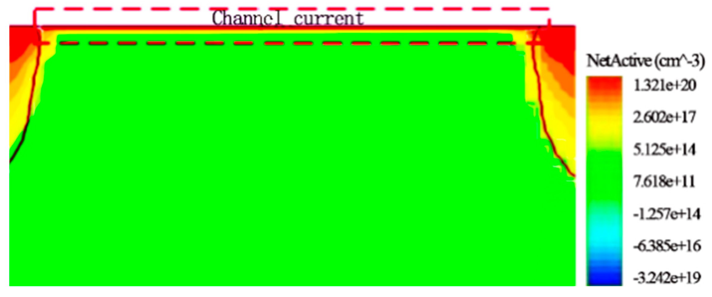
2. Device Description and Mechanism Analysis [1]

The conventional LTDDSCR is shown in Figure 1a: since DDSCR is symmetric, it has the same positive and negative ESD pulse paths. The conventional LTDDSCR optimizes the trigger voltage by changing the avalanche breakdown position of a P+ trigger junction spanned between the trap regions. When the ESD pulses reach the IO1 port, the ESD conduction path is formed through the NPN and PNP with mutual positive feedback. However, the trigger voltage is not able to be further reduced because of avalanche breakdown mechanism.
To overcome the drawback above, STDDSCR is proposed in this paper, as shown in Figure 1b: It has a P-type trap with P+ and N+ active regions at each of the IO1 and IO2 ends, and an N-type trap region in the middle. The high-concentration P+ injection spanning between the trap region and the circular PB injection in the N-type trap region constitutes a pair of PMOS. A hole is opened in the center of the circular PB injection of N+ injection, which is connected to an N-type trap region. Different from the static breakdown characteristics of the avalanche breakdown, the STDDSCR structure employs an RC trigger circuit to further reduce the trigger voltage. By detecting the capacitor charging during the ESD pulse, the voltage at both ends of the capacitor gradually rises to generate a voltage difference at the gate source of the PMOS, thereby enabling the PMOS to be turned on and provide the conduction current for the SCR device. Consequently, the STDDSCR structure can be activated in advance without a large ESD pulse voltage, reducing the trigger voltage. A wire is connected to the N+ injection region of the N-well to the RC resistive coupling circuit and the gate side of the PMOS to assist in device triggering [11,12].
The RC trigger circuit activates the ESD device by detecting the instantaneous ESD pulse signal. Typically, the rise time of ESD pulse is less than 10 ns, while the power-on time of the power supply is 1 ms. Therefore, it is essential to establish an appropriate RC value, known as a time constant τ. Based on experience, the recommended RC value is approximately 1 μs, with R = 30 kΩ and C = 30 pF.
Figure 2 shows the STDDSCR equivalent circuit. When a forward ESD pulse reaches the device IO1 port, the capacitor of the RC trigger circuit is charged with the PN of Q3, as shown in Figure 2a. The capacitor charging equation is shown in (1).
V G = V 0 1 e t R C
Here, V 0 = V i n 0.7 , V G is the gate voltage of the PMOS. The capacitive voltage of the external RC trigger circuit is applied to the PMOS gate and grounded at the initial time. Since the voltage between the gate and substrate of the PMOS is less than V t h p = 1 , the PMOS conducts and generates a current discharge path earlier, as shown by the green line in Figure 2b. The current flowing through R2 after PMOS conduction is (2).
I = V i n R 1 + R M 1 + R M 2 + R 2
As the pulse voltage increases, the channel current is unable to meet the requirements, then the PN junction of Q3 has an avalanche breakdown, and the SCR positive feedback path formed by PNP and NPN transistor is used as the main current conduction path to release current [13,14]. This is shown by the yellow line in Figure 2b.

3. Simulation Analysis and Discussion

In order to facilitate the simulation and analysis of STDDSCR structure in TCAD, the gate voltage of the PMOS pair was fixed, as shown in Figure 3. Figure 4 shows the overall version of the structure. The SCR layout uses inserted finger distribution, where the resistance consists of the square kΩ/□ resistor and the capacitor is a two-layer metal MOS capacitor. The metal layer below the PAD connects to the RC trigger circuit, and the metal layer above the PAD is connected to the IO port. The structure is biaxially symmetrical, allowing the ESD current to be discharged simultaneously from both sides of the finger bar.

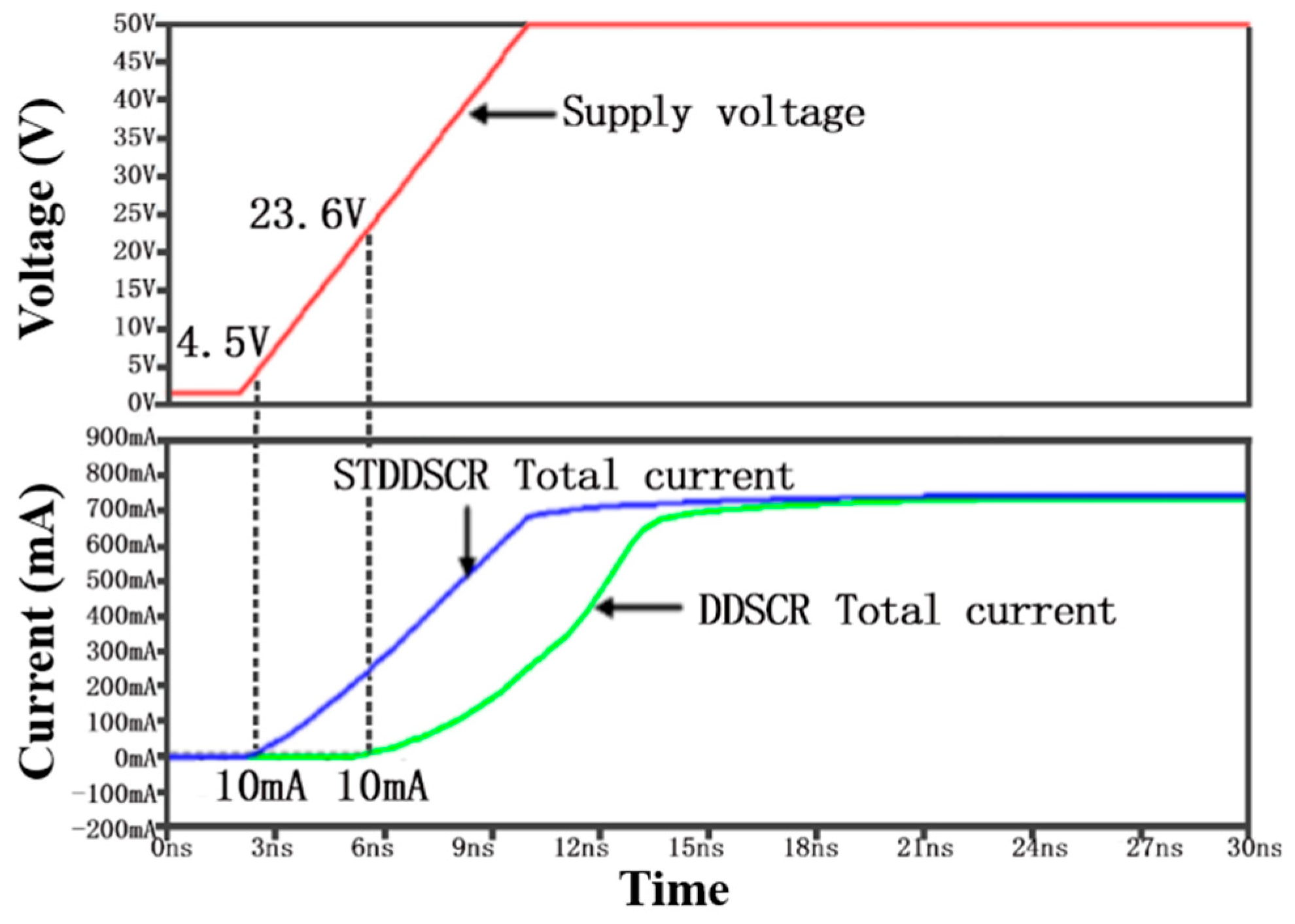
3.1. Overall Circuit Optimization Simulation Verification

LTspice simulation was performed for the extracted STDDSCR circuit diagram. To verify that the external RC trigger circuit achieves trigger voltage reduction, a TLP pulse voltage with a rising edge of 10 ns, a duration of 100 ns, a voltage of 50 V, and an internal resistance of 50 Ω was applied to the IO1 ends of the conventional DDSCR and STDDSCR structures, respectively. Figure 5 shows the variation of the voltage across the IO ports when a pulse was applied. With the increase in the pulse voltage, the voltage between IO port of STDDSCR structure is much lower than DDSCR at the same time, indicating that the RC trigger circuit achieves a further reduction in the trigger voltage. Figure 6 shows the total current versus supply voltage curves for the DDSCR and STDDSCR structures. Assuming that the device turns on when the total current in the circuit reaches 10 mA, we can know that when the device is on, the trigger voltage of the STDDSCR structure and DDSCR is 4.5 V and 23.6 V, respectively. The current curve shows that the STDDSCR has a lower trigger voltage compared to the DDSCR.

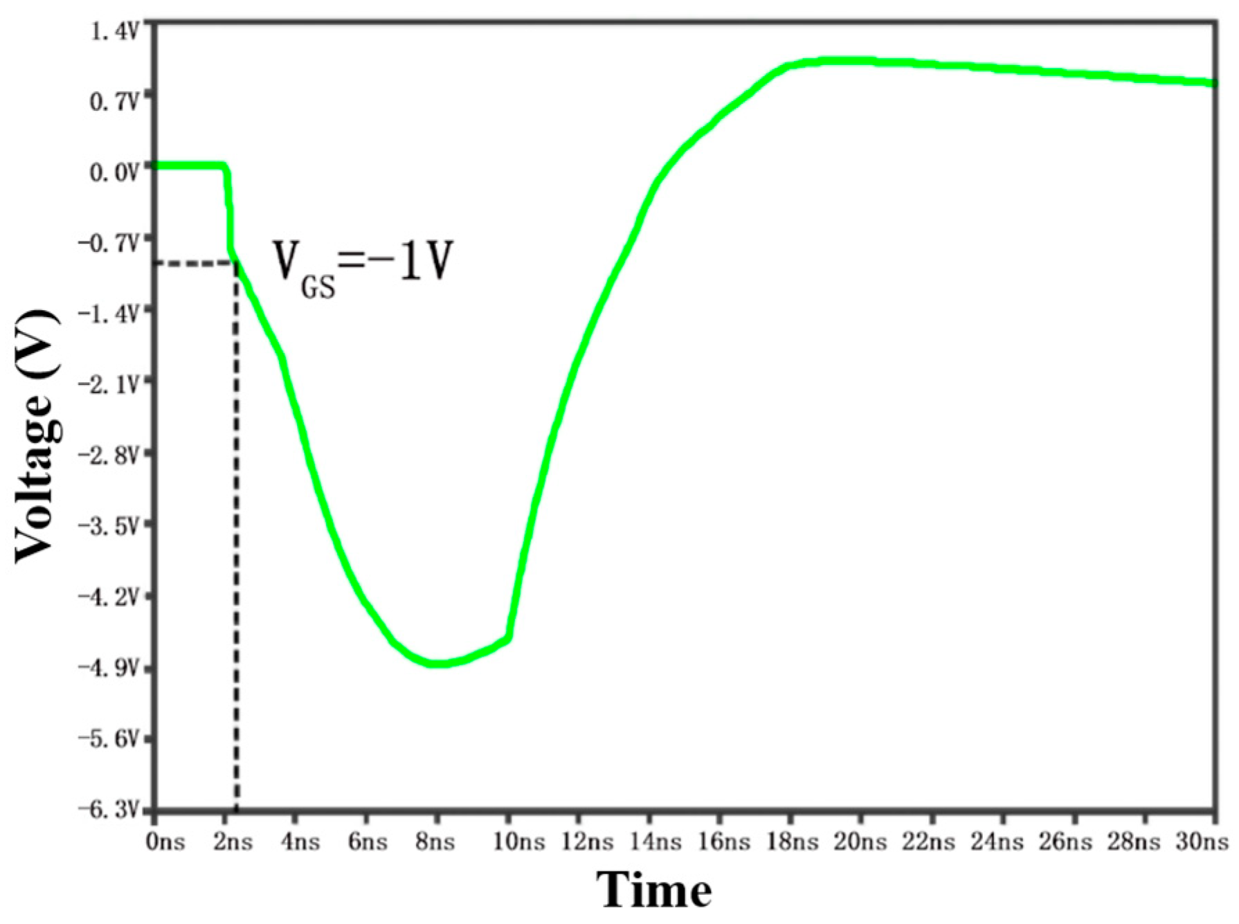
3.2. Fixed Gate Source Voltage Reasonableness Verification

The working principle of the device is further explored by TCAD software (Sentaurus TCAD). The threshold voltage of PMOS in STDDSCR structure is set to −0.8 V. Figure 7 shows the gate-source voltage of PMOS varies with time. In order to verify the effect of trigger junction on reducing trigger voltage in TCAD simulation, the fixed gate-source voltage V G S = 1   V was taken, at which time the PMOS starts to conduct. Figure 8 shows the I–V curves of the three structures under the same process simulation conditions. As we expected, the LTDDSCR trigger voltage of P-type trigger junction is lower than that of traditional DDSCR, and the STDDSCR structure further reduces the trigger voltage. Therefore, the simulation results show that two trigger units in the STDDSCR structure can effectively reduce the trigger voltage.
Figure 9 shows the TCAD simulation profile of the device. Figure 10 shows the current path of the device when it is fully on. We can see that when a pulse is applied to the IO1 end, the device is fully conducted and enters the clamping state. The current path at this moment is the SCR conduction path. The function of the trigger junction in the device is further analyzed. Figure 11 shows the collisional ionization diagram of the device.
The avalanche breakdown of the device occurs at the PB injection of the IO2 port, where the PB injection acts as a trigger junction and changes the location of the avalanche breakdown. For the PMOS in the device, Figure 12 shows the image of the cavity current at the PMOS channel when the gate source voltage is −1 V. There is a conductive channel under the PMOS, which provides channel current to facilitate the conduction of the SCR loop.

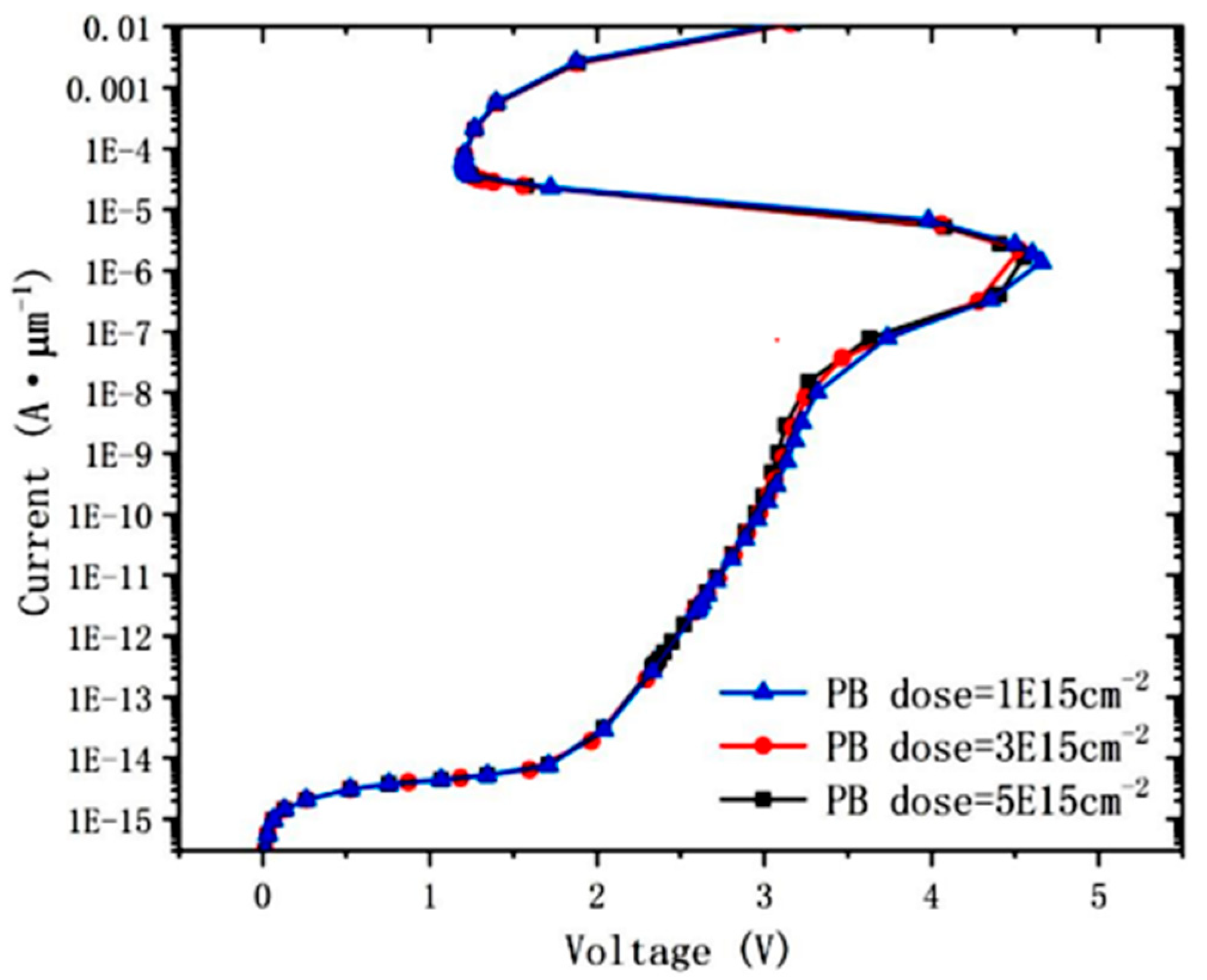
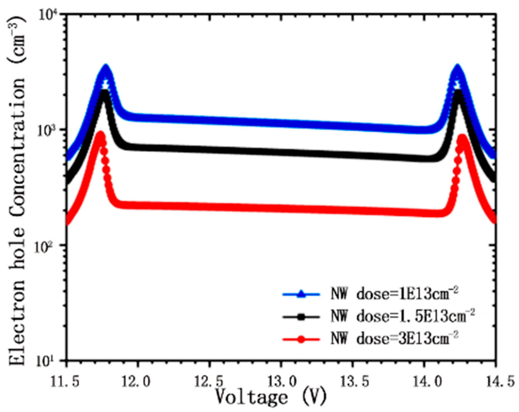
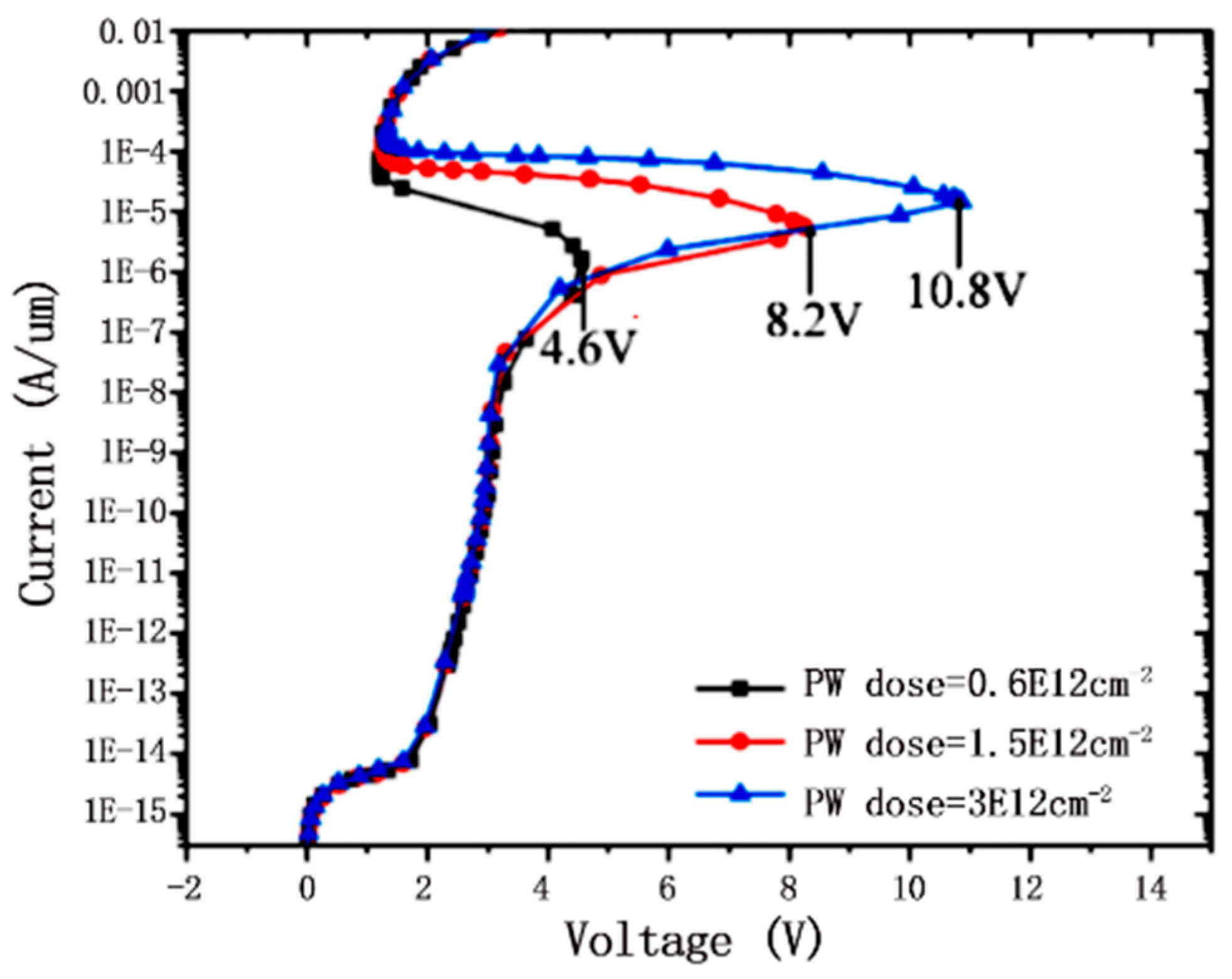
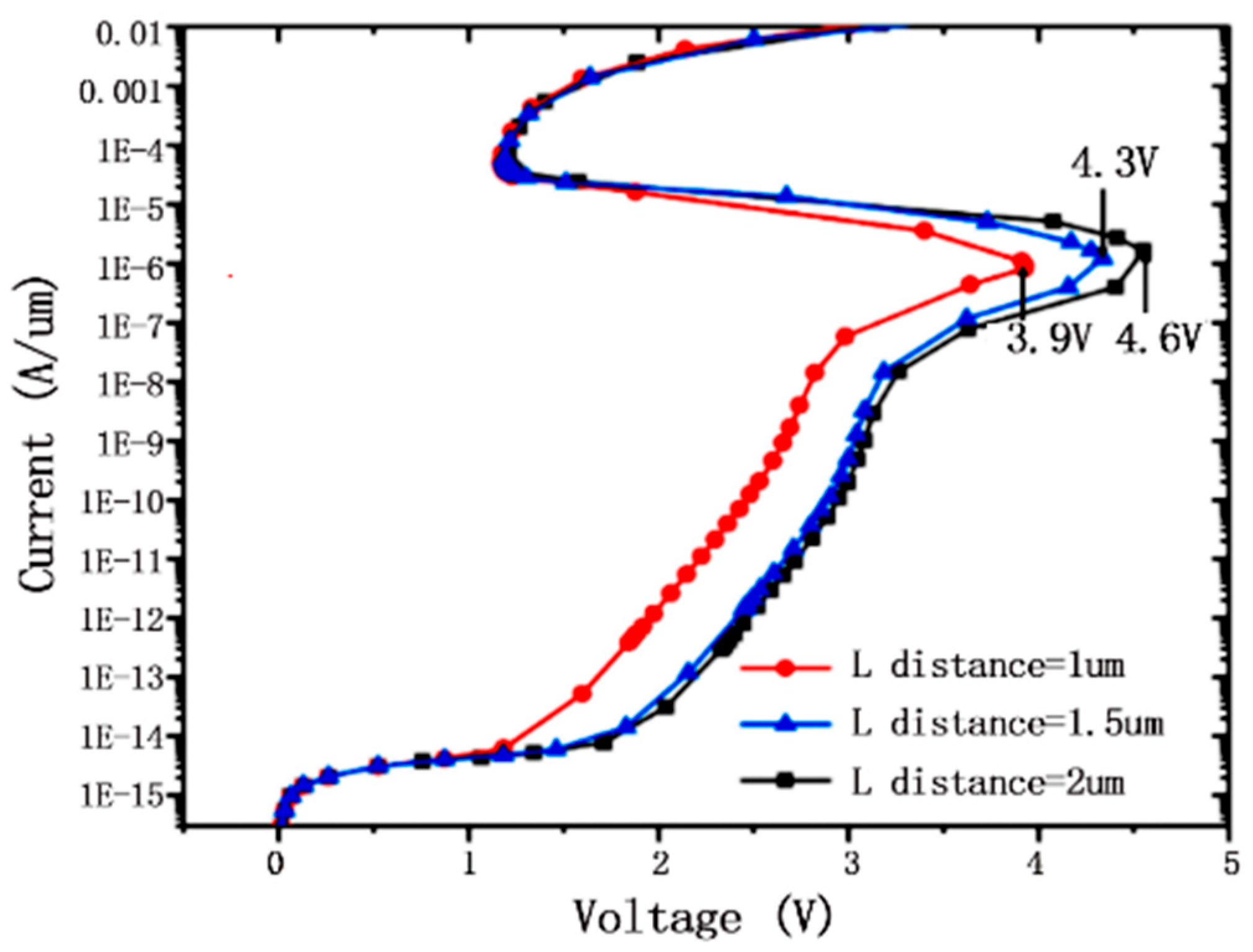
3.3. STDDSCR Parameter Optimization Simulation

Figure 13 shows the I–V curves of different PB injection concentrations. As we can see, the trigger voltage hardly changes for different PB injection doses. This structure has a small leakage of 1E14 A/μm level at 1.5 V operation, but a large leakage at 3.3 V operation. Thus, it can be used for ESD protection of 1.5 V high-speed ports.
In order to obtain a smaller threshold voltage, the injection dose of N-well is also small. The N-well serves as both the low concentration side of the trigger junction and the substrate of the PMOS pair. According to formula (3), the potential difference between the intrinsic Fermi level and quasi-Fermi level of N-type semiconductor is
Φ f n = V t ln N d n i
Increasing the NW injection dose will increase Φ f n , and the MOS threshold for N-type substrate is shown in (4)
V T H P = Q S D max Q S S t o x ε o x + Φ m s 2 Φ f n
Formulas (3) and (4) indicate that the change in N-well injection concentration will change the trigger voltage and the threshold voltage of PMOS. As shown in Figure 14, the trigger voltage decreases as the N-well injection concentration increases. However, a greater concentration of NW injection is not always better. Figure 15 shows a variation curve of hole concentration under PMOS with different concentrations of N-well. Contrary to Figure 14, the hole concentration under PMOS decreases as the N-well injection concentration increases. This indicates that the threshold voltage of PMOS becomes larger due to the increase in Φ f n , making channel-opening difficult [see (3) and (4)]. Therefore, the concentration of N-well injection needs to be strictly controlled.
As the base of the NPN triode, the doping concentration of P-well is highly correlated with the transmission coefficient of the base region. Figure 16 shows the variation of the trigger voltage with different P-well injection concentrations. As shown in the figure, the increase in P-well injection concentration makes the NPN conduction difficult and the trigger voltage become higher. And when the PW injection dose is 0.6 × 1012 cm−2, a lower trigger voltage can be obtained. In the next test, the effect of the PMOS gate length on the trigger voltage was verified, as shown in Figure 17. Since the gate length directly determines the channel length of the PMOS, and the channel length affects the intensity of the channel current [see (5)], when the gate length L decreases, the conduction current provided to the SCR path becomes larger, and the trigger voltage of the device decreases. Note that the gate length should not be too short to avoid the PB injection region on both sides of the PMOS to be connected after annealing. Compared to the other two cases, the device with a length of 1μm starts to leak current at 1 V.
I D = W μ p C o x 2 L 2 V S G + V T H V S D V S D 2
The feasibility of the structure and the trend of each electrical parameter were verified by LTspice and TCAD simulation software. Finally, the optimal parameters are summarized in Table 1.

3.4. Discussion

This work is compared with the previous ESD protection structures in Table 2. Different from the other two structures, the proposed STDDSCR structure rapidly detects the ESD pulse and activates PMOS with RC trigger circuit, thereby generating the drain current of conducting channel in advance. The trigger voltage can be reduced to about 4.5 V. Moreover, the device has low capacitance characteristics by using high resistance epitaxy and low concentration of N-well injection. The device can be used for high-speed port ESD protection at 1.5 V and below.

4. Conclusions

In this paper, a bidirectional ESD protection device with ultra-low trigger voltage is designed. The external RC trigger circuit and trigger junction can simultaneously reduce the trigger voltage, allowing ESD devices to be turned on and clamped to transient high currents earlier. Compared with the traditional structure, this structure has a lower trigger voltage and is more suitable for ESD design Windows under low voltage. In addition, the simulation results show that the structure has less leakage when the operating voltage is 1.5 V, and can be used for ESD protection of 1.5 V and below.

Author Contributions

Conceptualization, F.L.; validation, J.P., L.W. and J.H.; investigation, J.H.; resources, J.P. and L.W.; data curation, J.J.; writing—original draft preparation, X.H. and J.H.; writing—review and editing, X.H.; visualization, X.H.; supervision, F.L.; project administration, F.L.; funding acquisition, J.P. and L.W. and J.H. All authors have read and agreed to the published version of the manuscript.

Funding

This research was funded by The Laboratory Open Fund of Beijing Smart-Chip Microelectronics Technology Ltd. grant number [NO. SGSC0000MNQT2207226].

Data Availability Statement

The original contributions presented in the study are included in the article, further inquiries can be directed to the corresponding author.

Acknowledgments

This work was supported by the Laboratory Open Fund of Beijing Smart-chip Microelectronics Technology Co., Ltd.

Conflicts of Interest

Author J.P., W.L., J.J. was employed by the company Beijing Smartchip Microelectronics Technology Company Limited. The remaining authors declare that the research was conducted in the absence of any commercial or financial relationships that could be construed as a potential conflict of interest. The authors declare that this study received funding from The Laboratory Open Fund of Beijing Smart-Chip Microelectronics Technology Ltd. The funder had the following involvement with the study: validation, resource, data curation and funding acquisition.

References

  1. Navid, R.; Chen, E.-H.; Hossain, M.; Leibowitz, B.; Ren, J.; Chou, C.-H.A.; Daly, B.; Aleksic, M.; Su, B.; Li, S.; et al. A 40 Gb/s Serial Link Transceiver in 28 nm CMOS Technology. IEEE J. Solid-State Circuits 2015, 50, 814–827. [Google Scholar] [CrossRef]
  2. Cui, Q.; Salcedo, J.A.; Parthasarathy, S.; Zhou, Y.; Liou, J.J.; Hajjar, J.J. High-Robustness and Low-Capacitance Silicon-Controlled Rectifier for High-Speed I/O ESD Protection. IEEE Electron. Device Lett. 2013, 34, 178–180. [Google Scholar] [CrossRef]
  3. Ker, M.-D.; Hsu, K.-C. Overview of on-chip electrostatic discharge protection design with SCR-based devices in CMOS integrated circuits. IEEE Trans. Device Mater. Reliab. 2005, 5, 235–249. [Google Scholar] [CrossRef]
  4. Chang, T.H.; Hsu, Y.Y.; Tsai, T.C.; Tseng, J.C.; Lee, J.W.; Song, M.H. High-k metal gate-bounded Silicon Controlled Rectifier for ESD protection. In Proceedings of the Electrical Overstress/Electrostatic Discharge Symposium Proceedings 2012, Tucson, AZ, USA, 9–14 September 2012. [Google Scholar]
  5. Lin, C.-Y.; Chang, R.-K. Design of ESD Protection Device for K/Ka-Band Applications in Nanoscale CMOS Process. IEEE Trans. Electron. Devices 2015, 62, 2824–2829. [Google Scholar] [CrossRef]
  6. Dong, A.; Salcedo, J.A.; Parthasarathy, S.; Zhou, Y.; Luo, S.; Hajjar, J.-J.; Liou, J.J. ESD protection structure with reduced capacitance and overshoot voltage for high speed interface applications. Microelectron. Reliab. 2017, 79, 201–205. [Google Scholar] [CrossRef]
  7. He, L.; Salcedo, J.A.; Parthasarathy, S.; Zhou, Y.; Hajjar, J.-J.; Sundaram, K. Compact and Fast-Response Voltage Clamp for Bi-Directional Signal Swing Interface Applications. IEEE Electron. Device Lett. 2018, 39, 1880–1883. [Google Scholar] [CrossRef]
  8. Wu, M.; Zhang, C.; Peng, W.; Xu, J.; Jin, H.; Zeng, Y.; Chen, Z. A Radiation-Hardened Dual-Direction SCR Based on LDMOS for ESD Protection in the Extreme Radiation Environment. IEEE Trans. Nucl. Sci. 2020, 67, 708–715. [Google Scholar] [CrossRef]
  9. Guan, J.; Wang, Y.; Hao, S.; Zheng, Y.; Jin, X. A Novel High Holding Voltage Dual-Direction SCR With Embedded Structure for HV ESD Protection. IEEE Electron. Device Lett. 2017, 38, 1716–1719. [Google Scholar] [CrossRef]
  10. Huang, X.; Liou, J.J.; Liu, Z.; Liu, F.; Liu, J.; Cheng, H. A New High Holding Voltage Dual-Direction SCR With Optimized Segmented Topology. IEEE Electron. Device Lett. 2016, 37, 1311–1313. [Google Scholar] [CrossRef]
  11. Do, K.-I.; Song, B.-B.; Koo, Y.-S. A Novel Dual-Directional SCR Structure with High Holding Voltage for 12-V Applications in 0.13-μm BCD Process. IEEE Trans. Electron. Devices 2020, 67, 5020–5027. [Google Scholar] [CrossRef]
  12. Do, K.-I.; Koo, Y.-S. A New SCR Structure with High Holding Voltage and Low ON-Resistance for 5-V Applications. IEEE Trans. Electron. Devices 2020, 67, 1052–1058. [Google Scholar] [CrossRef]
  13. Liang, H.; Gu, X.; Dong, S.; Liou, J.J. RC-Embedded LDMOS-SCR With High Holding Current for High-Voltage I/O ESD Protection. IEEE Trans. Device Mater. Reliab. 2015, 15, 495–499. [Google Scholar] [CrossRef]
  14. Yang, Z.; Liu, H.; Wang, S. A low leakage power-rail ESD detection circuit with a modified RC network for a 90-nm CMOS process. J. Semicond. 2013, 34, 45010. [Google Scholar] [CrossRef]
Figure 1. Structural profile. (a) DDSCR. (b) STDDSCR.
Electronics 13 03458 g001
Figure 2. STDDSCR structure equivalent circuit. (a) RC trigger circuit works. (b) SCR pathway.
Electronics 13 03458 g002
Figure 3. Equivalent profile of STDDSCR with fixed gate voltage.
Electronics 13 03458 g003
Figure 4. Overall version of STDDSCR structure.
Electronics 13 03458 g004
Figure 5. Voltage at both ends of DDSCR and STDDSCR structures.
Electronics 13 03458 g005
Figure 6. Total current vs. supply voltage curves for DDSCR and STDDSCR structures.
Electronics 13 03458 g006
Figure 7. Gate-source voltage of PMOS varies with time.
Electronics 13 03458 g007
Figure 8. I–V curves for DDSCR, LTDDSCR, and STDDSCR structures.
Electronics 13 03458 g008
Figure 9. TCAD simulation profile of the device.
Electronics 13 03458 g009
Figure 10. Current path when the device is full on.
Electronics 13 03458 g010
Figure 11. Device avalanche breakdown location.
Electronics 13 03458 g011
Figure 12. Image of cavity current under PMOS.
Electronics 13 03458 g012
Figure 13. I–V curves for different PB injections.
Electronics 13 03458 g013
Figure 14. I–V curves for different N-well injection concentration.
Electronics 13 03458 g014
Figure 15. Hole concentration curves under PMOS.
Electronics 13 03458 g015
Figure 16. I–V curves for different P-well injection concentration.
Electronics 13 03458 g016
Figure 17. I–V curves for different gate length L.
Electronics 13 03458 g017
Table 1. Optimal parameters.
Key ParametersNumerical Value
NW dose/cm21.5 × 1013
PW dose/cm20.6 × 1012
L length/μm1.5
Resistance/kΩ30
Capacitance/pF30
Table 2. Trigger voltage comparison.
Device StructureTrigger Voltage/VHold Voltage/VLeakage Current at 25 °C (nA) @1.5 V
DDSCR23.91.2310
LVTDDSCR14.81.25<1
DCSCR1.821.3>1000
STDDSCR (Proposed)4.61.26<1
Disclaimer/Publisher’s Note: The statements, opinions and data contained in all publications are solely those of the individual author(s) and contributor(s) and not of MDPI and/or the editor(s). MDPI and/or the editor(s) disclaim responsibility for any injury to people or property resulting from any ideas, methods, instructions or products referred to in the content.

