Article

Frequent Power-Up-and-Down-Induced Degradation of Device and Bandgap Voltage Reference in 14-nm FinFET Technology

School of Microelectronics, Fudan University, Shanghai 200433, China
*
Authors to whom correspondence should be addressed.
Electronics 2024, 13(17), 3506; https://doi.org/10.3390/electronics13173506
Submission received: 4 July 2024 / Revised: 30 August 2024 / Accepted: 2 September 2024 / Published: 4 September 2024

Abstract

:
The need for low power consumption in highly integrated systems-on-chip (SoCs), such as IoT-based smoke detection systems, has made frequent power-ups and power-downs a common practice. Although the device performance degradation caused by such frequent power-ups and power-downs is ignored in most circuit studies, in high-precision bandgap voltage references, the degradation of particular devices can result in a reference voltage shift. This work investigates the effects of frequent power-ups and power-downs on a simple bandgap reference circuit and demonstrates that the effects are real and non-negligible. Aging simulations based on simple bandgap reference circuits are performed to analyze the causes of device performance degradation and circuit output voltage shifts. The simulation results show that frequent power-ups and power-downs induce the negative bias temperature instability (NBTI) effect, a phenomenon that causes performance degradation in devices, such as threshold voltage degradation, under negative bias and high temperature conditions. Further, gate voltage waveforms of these devices were extracted for aging tests and the results of the tests in 14 nm FinFET and the NBTI aging model were used to infer the threshold voltage shift after 10 years at 125 °C. A circuit modification is proposed to mitigate the degradation of device performance and reference voltage shift. This work indicates that NBTI stresses introduced by frequent power-ups and power-downs need to be considered in circuit design.

1. Introduction

With the rapid advancement of system-on-chip (SoC) technology, the pursuit of high performance, large scale, and high integration has made the system power consumption a great challenge [1]. Low-power SoCs often utilize power management modules to switch parts of the circuitry that are temporarily not required into a power-down mode [2,3]. This approach allows for efficient power utilization and helps meet the increasingly high performance and low power consumption requirements in modern SoCs. As an example, the SoC for smoke detection integrates a series of sensors such as temperature and humidity, which are detected at regular intervals to achieve real-time monitoring and response to changes in the environment while also reducing power consumption [4,5]. However, this approach to reduce power consumption leaves some of the functional circuits to be powered up and down frequently, leading to reliability issues as the performance of the devices in the circuit degrades.
Frequent power-down-and-power-up-induced device degradation has not been a concern in circuit studies due to the fact that for most of the circuit modules, the aging of the devices in the power-down circuits does not affect the circuit performance or the effect is negligible. However, for bandgap voltage references, the start-up circuit connected to the power-down circuit directly affects the bias current [6], high-precision bandgap voltage references with output accuracy at the ppm level are sensitive to the absolute value of the bias current, and device degradation caused by frequent power-ups and power-downs cannot be ignored.
According to the existing research on the mechanism of device degradation, directly related to the device degradation caused by frequent power-ups and power-downs is negative bias temperature instability (NBTI) [7,8,9], which refers to the progressive degradation of various electrical parameters, including threshold voltage and saturation current, in p-channel devices due to the prolonged application of negative gate bias [10,11]. The research of NBTI-induced circuit reliability degradation primarily focusses on digital circuits and frequency-dependent circuits like PLL and oscillator circuits. This emphasis stems from the fact that the gate voltage and drain voltages in these circuits often exhibit magnitudes that are close to the power supply voltage [12,13,14]. In analog circuits, the primary consequence of NBTI on circuit reliability manifests in device mismatches under varied gate biases. Specifically, this leads to output delays in comparators, output voltage decreases in amplifiers, and mismatches in current mirrors [15,16,17,18,19]. However, it is worth noting that the causes of NBTI effects in the existing studies are due to the prolonged operation of the circuits rather than frequent power-ups and power-downs, and that the circuit reliability analyses are limited to simulations relying on the NBTI aging model and lack data from actual tests. Transient start-up currents occur in circuits under frequent power on/off cycles, generating Joule heat that can cause localized temperature rises. Concurrently, devices experience significant negative gate bias during repeated power-ups and power-downs. Both of these phenomena accelerate NBTI degradation, making the accurate modeling of degradation effects crucial for predicting device longevity and reliability. Further research is needed to fill gaps on the effect of frequent power-ups and -downs on performance degradation in circuits. Insights into circuit degradation can be gained by analyzing the aging of specific devices within the overall circuit, providing a deeper understanding of bandgap reference shifts due to frequent power-ups and power-downs. Therefore, anti-aging studies are conducted on a bandgap reference with repeated power-ups and -downs for smoke detection SoCs in FinFET technology. Compared to standard CMOS, FinFET technology has specific characteristics such as better energy efficiency and greater resistance to parameter variability, making it more suitable for high-density, high-performance, and low-power applications. Additionally, FinFETs offer better channel control and reduced leakage currents, which are crucial factors when studying NBTI effects.
In this paper, the effect of frequent power-ups and power-downs on the output shift of a bandgap reference circuit is investigated through aging simulations of a simple bandgap voltage reference circuit and aging tests of a p-FinFET device under NBTI stress. The aging simulation of the bandgap reference circuit is used to identify a specific device that causes the reference voltage to shift during frequent power-ups and power-downs. Based on the simulated waveforms of the device gate, NBTI stress is applied to actual devices manufactured using the 14 nm FinFET process. Aging tests are then conducted to estimate the threshold voltage shift of these devices after 10 years of exposure to this stress at 125 °C. The reasons for circuit degradation caused by this device are analyzed, and the circuit is improved to reduce NBTI degradation. Our study provides a more comprehensive understanding and analysis of analog circuit degradation caused by power-ups and -downs, offering guidance for circuit design and reliability assessment.

2. NBTI Degradation Model

NBTI refers to the degradation of electrical parameters in p-FETs that occurs when a negative gate voltage is applied at high temperatures. On the nanometer scale, the impact of NBTI on electrical parameters such as threshold voltage shift and saturation current reduction becomes increasingly severe. Extensive research has been conducted to investigate the influence of these parameter degradations on analog circuits. Although there is ongoing debate about the precise mechanisms of NBTI degradation, there are widely acknowledged factors contributing to NBTI effects [20]. These include interface trap formation, hole trapping in the oxide layer, and bulk trap generation [15]. All of these mechanisms are intricately linked to the manufacturing process and stress conditions. Here, the degradation model of NBTI is described in [21,22]:
Δ V TH = A   ×   e E a kT   ×   e m V gs   ×   t n
where Ea is the activation energy, k is Boltzmann’s constant, Vgs is the applied gate-source voltage, and T and t are the aging temperature and time, respectively. A is a constant related to the process. m and n are acceleration exponential factors for gate source voltage and time, with n being 0.2 in the simulation. Based on the degradation model, the evaluation of threshold voltage shift at low voltages can be performed through device aging tests that are accelerated by applying high gate voltages and can also be extrapolated for long time aging threshold voltage shift.

3. Results and Discussion

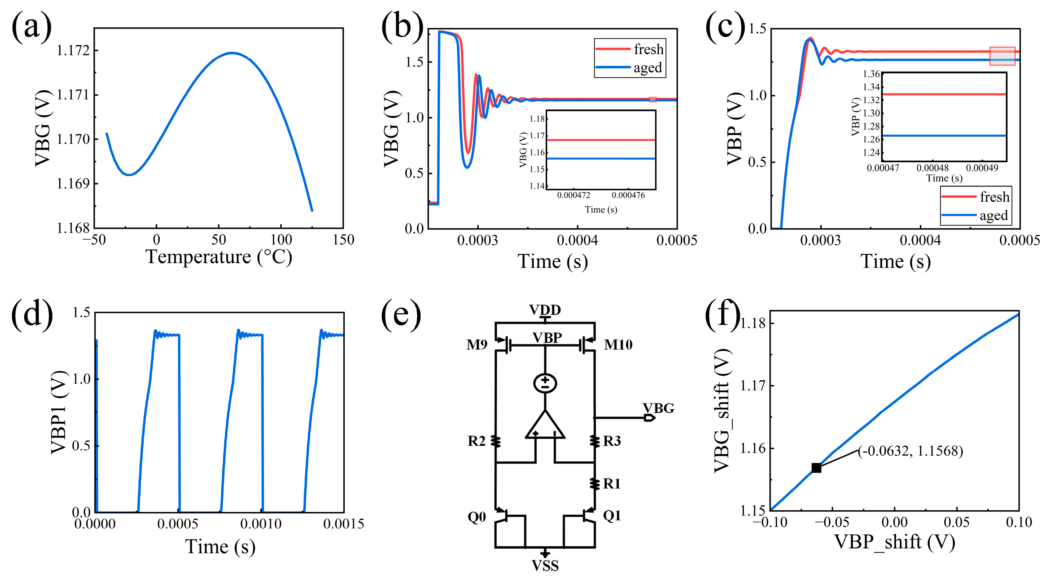
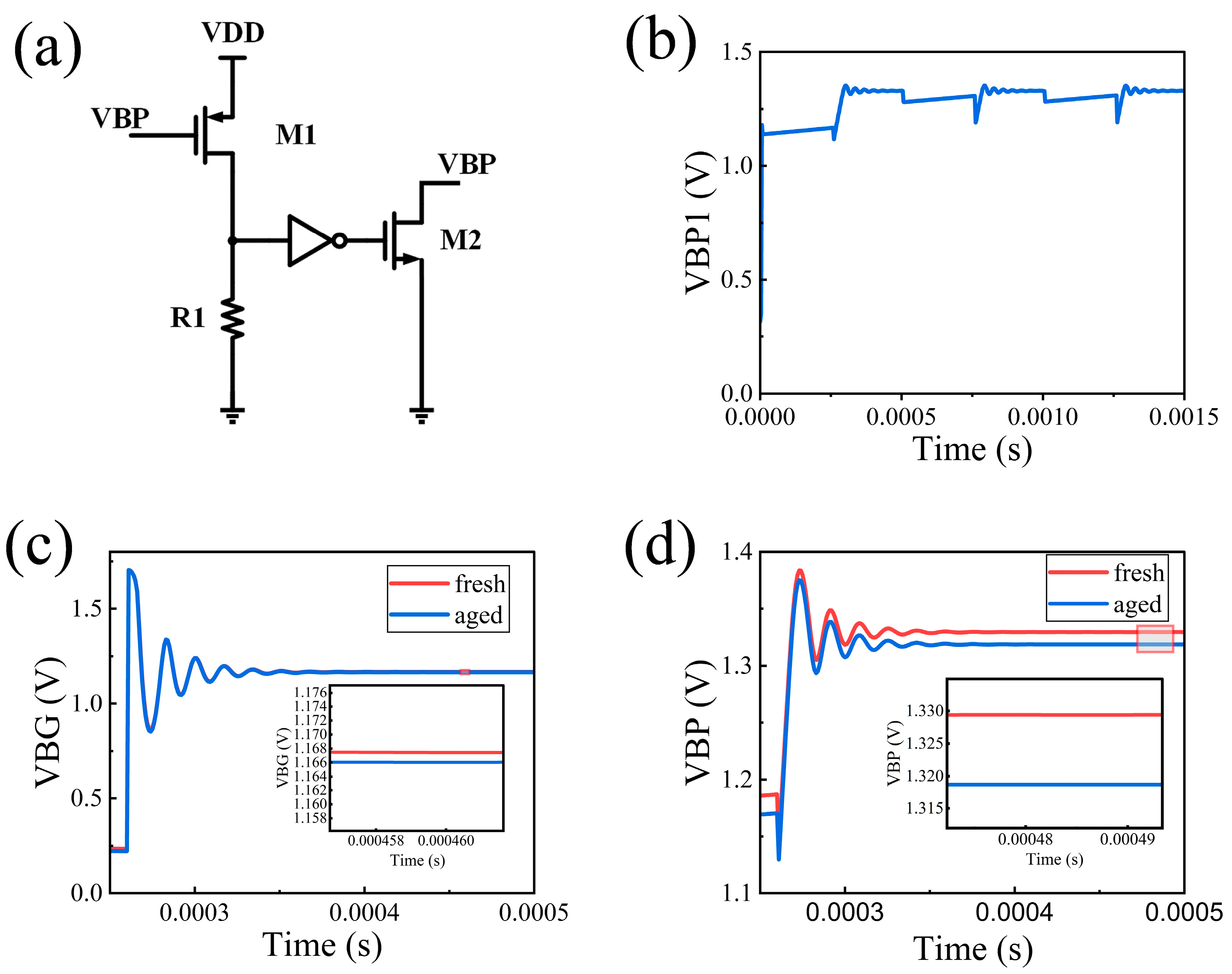
3.1. Circuit Modules and Simulation

3.1.1. Configurations of Simulated Bandgap Voltage Reference

The schematic of the proposed bandgap reference circuit is shown in Figure 1a. The overall circuit architecture consists of the core circuit with a Proportional to Absolute Temperature (PTAT) current generation scheme, a start-up circuit, and choppers. The base-emitter voltage VBE of the BJT exhibits a negative correlation with temperature. The aforementioned core circuit combines the linear PTAT voltage generated by the PTAT current and the VBE with an appropriate scaling factor to generate a voltage that remains independent of temperature, power supply, and process variations.
As shown in Figure 1b, the PTAT current generated by the core circuit is:
I PTAT   = V T ln n R 1
where VT is the thermal voltage and n is the area ratio of BJT Q0 and Q1. Then, the PTAT current flows through R1 and R3 and generates bandgap reference voltage VREF with VBE1 of BJT Q1, as follows:
V REF   = V T ln n · R 1 + R 3 R 1 + V B E 1
where the VT is proportional to temperature and VBE1 is negatively correlated with temperature. Thus, the two terms of the equation have positive and negative temperature coefficients, respectively. The PTAT voltage can be scaled by adjusting the coefficient associated with n, R1, and R3 to compensate for the voltage VBE1 with a negative temperature coefficient and generate the reference voltage VREF. This equation embodies the principle of voltage compensation based on temperature coefficients [6].
The operational amplifier of the core circuit is used to maintain the voltage levels at its two inputs approximately equal. Since the offset voltage at the two inputs of the op-amp directly affects the magnitude of the PTAT current, leading to the accuracy degradation of the bandgap voltage reference, choppers are used to periodically switch the input signals at the two inputs to reduce DC offset errors and improve the precision [23]. The filter at the output of the op-amp is used to average the output voltages at the OUTP and OUTN outputs. The load n-channel FinFETs are biased by M13 and M14.
In the bandgap voltage reference circuit, when the value of the voltage at the BP1 node is close to the supply voltage, the absence of current in the circuit signifies a specific steady state not intended. In order to avoid the state and to increase the start-up speed of the circuit, the start-up circuit in Figure 1c is applied. In the scenario where the enable signal EN is at the voltage level of VSS, the bandgap voltage reference circuit operates in a zero current mode. During this mode, the voltage at the VBG node closely approximates VSS and transistor M11 turns off while transistor M12 turns on, causing the BP1 node to be pulled down to the VSS level. This sequence allows the circuit to initiate its normal operation. It should be noted that the start-up circuit does not interfere with the normal operation of the circuit.
The circuit is simulated using the 14 nm FinFET process. The length of the devices in the PDK is limited, so to achieve the required size, nine devices are connected in series as a single device, as shown in Figure 1d.

3.1.2. Aging Analysis and Problem Identification

By using the Semiconductor Manufacturing International Corporation (SMIC) 14 nm FinFET process to simulate the proposed bandgap voltage reference, the results of the temperature variation of the pristine circuit and degraded circuit after 10 years of aging at 125 °C are shown below. The simulation of this circuit was conducted under a power supply voltage of 1.8 V. To emulate the frequent power-up process of the bandgap voltage reference in practical scenarios, a square wave signal was utilized as the enable signal. This signal ranged from 0 V to 1.8 V with a period of 500 μs and a pulse width of 250 μs. In this section, the devices cause degradation of the circuit will be discussed.
Figure 2 indicates the results of pre-layout simulation. Figure 2a shows the variation in VREF with temperature for the bandgap voltage reference. The VREF is 1.17 V at 25 °C and the temperature coefficient is 18.3 ppm/°C from −40 °C to 125 °C, with a maximum value of 1.172 V and a minimum value of 1.168 V. The temperature coefficient of the bandgap reference is calculated using the following equation:
TC = VRE F max VRE F min Δ Temperature   ·   VRE F average · 10 6
Figure 2b illustrates the output curve of the bandgap voltage reference at VBG node within 500 μs after the circuit is turned on. The red curve corresponds to the VBG’s output voltage curve before aging, while the blue curve represents the output voltage curve after subjecting the circuit to the specified stresses, aging at 125 °C for 10 years. It is observed that the output of the bandgap voltage reference is reduced by about 10 mV after aging. Bandgap references are essential in integrated circuits for precision applications such as ADCs (analog-to-digital converters) and voltage regulation circuits. However, even minor variations in voltage can compromise the system’s accuracy and reliability, potentially leading to malfunctions or reduced performance. For instance, in high-precision, low-speed incremental Delta-Sigma ADCs used for measurement, slight shifts in the reference voltage can result in inaccuracies during the analog-to-digital conversion process, causing output errors. Figure 2c,d show the voltage waveforms at the VBP node within 500 μs of circuit start-up and the aging stress on the VBP during aging, respectively. A voltage reduction of about 80 mV is observed at VBP. A voltage source is added to VBP to verify if this reduction leads to the output voltage reference shift, as shown in Figure 2e. Figure 2f shows the shift of VBG as the shift of VBP varies from −100 mV to +100 mV, and the data point at VBP = −63 mV matches the output VBG value after aging. The reference voltage at the output of the circuit after the aging simulation is 1.156 mV, which is the same as the reference voltage of the circuit after the VBP node voltage is reduced by 63 mV. This indicates that it is indeed the aging of the device associated with the VBP node voltage that is causing the reference voltage to shift.
A substantial degradation of devices M2, M9, M10, and M15 is evident from the simulation results, showing threshold voltage shifts exceeding 10 mV. During circuit operation in the power-down mode, the Vgs for these P-channel FinFETs notably increases, approaching the supply voltage. Each series-connected device composing M2, M9, M10, and M15 operates with millivolt-level Vds (source-drain voltage) and approximately 1 µA Ids (source-drain current). These conditions—high Vgs and low Vds and Ids—confirm that the devices are undergoing NBTI stress rather than HCI (hot carrier injection) stress. Hot carrier injection stresses arise due to interfacial states induced by drain avalanche carrier injection, and the stress conditions are characterized by high Vgs, Vds, and Ids [24].
In the bandgap reference circuit, the gates of FinFETs M2, M9, M10, and M15 are connected to the VBP node. As these devices experience an increase in threshold voltage due to NBTI stress, the VBP node level decreases to maintain their saturated operating state. Consequently, this induces a further negative bias on the gates of the devices, exacerbating the NBTI effect. Simultaneously, it disrupts the circuit’s static operating point and introduces mismatches in the bandgap reference op-amps, causing a shift in the output reference voltage.

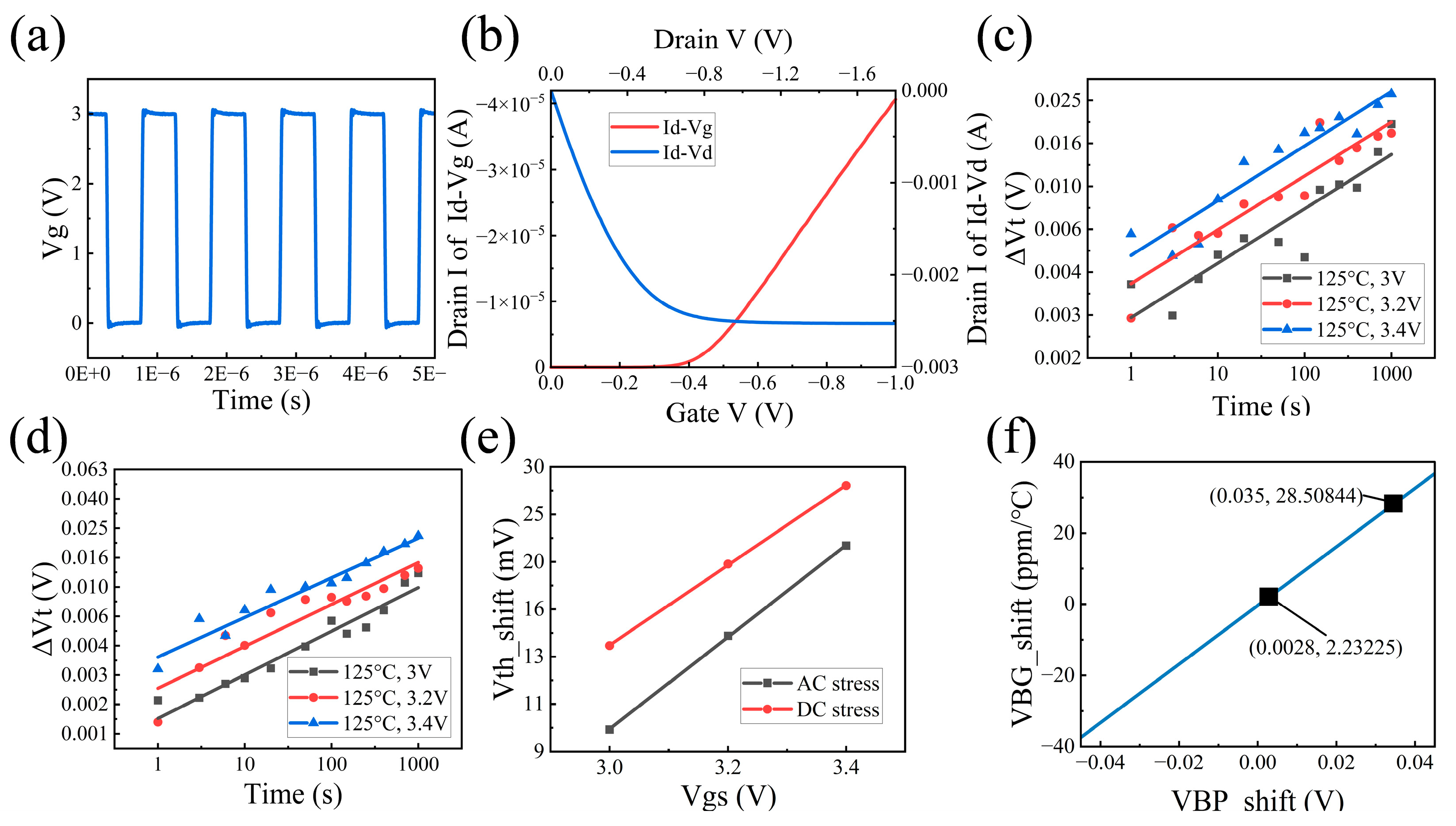
3.2. Device Aging Test Results and Discussion

Individual device aging tests were performed to validate the existence of NBTI aging in the simulation and to derive the device subthreshold voltage shift for practical applications. The FinFET devices tested in this work are core devices fabricated based on the SMIC FinFET process platform. The typical device has 14 fins, with a fin height of ~30 nm, a fin top width of ~10 nm, and an effective gate length of ~15 nm. NBTI stress is applied on p-channel FinFET with voltage acceleration using alternating gate bias at the temperature of 125 °C for 1000 s to represent the frequent power-ups of M2 in the bandgap voltage reference circuit. The drain, source, and well electrodes are biased at the supply voltage to prevent other degradation effects caused by excessive source-drain current during the stress process. The high level of the square wave of the gate stress varies between 3 V and 3.4 V to ensure that the degradation of the threshold voltage can be measured and that the gate dielectric breakdown does not occur.
The degradation of the p-channel FinFET is observed by threshold voltage shift with a stress-measure-stress technique [25,26]. Stress is applied at logarithmic time intervals with periodic interruptions to measure the drain current at a fixed voltage input of 0 V at the gate, 1.79 V at the source, and 1.8 V at the drain and well electrodes. The threshold voltage shift is extracted by linearly interpolating the Id-Vg curves based on the measured drain current.
Figure 3 shows the conditions and results of the aging test. Figure 3a depicts the gate bias waveform during actual testing. Figure 3b presents the original Id-Vg and Id-Vd characteristics of the device being tested. Figure 3c illustrates the temporal variation in the Vth shift during a 1000 s aging test, where the gate input is a square wave with different high levels. Logarithmic scales are employed for both the horizontal and vertical axes. By applying logarithms to both sides of Equation (1), a linear fit can be performed on the obtained data. The average slope of the resulting curve is determined to be 0.283, which represents the tested value of the time exponent n in Equation (1). Figure 3d illustrates the relationship between the shift value of Vth and time when the gate is grounded. After applying logarithmic transformations and performing linear fit analysis, the resulting slope is determined to be 0.253. Figure 3e displays the fitting of the Vth shift over 1000 s, extracted from Figure 3c and Figure 3d, respectively. The fitting is performed based on the relationship between the Vth shift and Vgs, as described in Equation (1). Figure 3f is optimized from Figure 2f and represents the voltage shift of the bandgap reference output with respect to the VBP node voltage, where the shift is calculated by substituting into Equation (4) to obtain the ppm level of variation.
The average slopes obtained from the linear fit analysis in Figure 3c,d are 0.283 and 0.253, respectively. According to Equation (1) and related illustration, these values correspond to the time acceleration exponential factor n. Typically, n assumes a value around 0.2 in the context of NBTI effects. In contrast, existing studies have shown this acceleration exponential factor to be above 0.5 in the HCI effect [27]. Thus, the results affirm that device aging is predominantly influenced by NBTI rather than HCI.
Based on the VBP waveform acquired through simulation and the fitted curve depicted in Figure 3e, it is possible to extrapolate the results. It can be inferred that when Vgs is a square wave with a high level of 1.8 V, the shift value of Vth after 1000 s of aging at 125 °C is estimated to be 0.969 mV. Furthermore, by extrapolating from the curve presented in Figure 3c, the shift value of Vth is projected to reach 34.9 mV after 10 years, which corresponds to a bandgap reference accuracy degradation of 28.5 ppm/°C according to Figure 3f. Similarly, by extrapolating from Figure 3d, if the measured device is subjected to prolonged bias with a negative gate voltage of 1.8 V, the anticipated shift value of Vth after 10 years is determined to be 45.8 mV.
The threshold voltage shifts observed in M2, M9, M10, and M15 during frequent power-ups of the bandgap reference can be attributed to the substantial negative bias applied to the gate. This negative bias results from VBP approaching VSS during the power-down state. To mitigate this degradation, a modification was made to the original circuit’s start-up circuit, as depicted in Figure 4a. In this modified circuit, when the supply voltage is 0 V, VBP is also 0 V. Upon power-up, M1 is turned off, M2 is turned on, and VBP is pulled up, enabling normal circuit operation. Consequently, M2 remains in the “on” state while M1 remains in the “off” state, thus ensuring that the normal operation of the circuit is not disrupted. During power-down, the effect of the enable terminal causes VBP to be close to VDD. As shown in Figure 4b, the modified start-up circuit results in a voltage waveform of VBP floating around 1.3 V, with corresponding Vgs values of M2, M9, M10, and M15 only reaching 0.5 V. Figure 4c,d demonstrate that the modification of the start-up circuit significantly reduces the shift of VBG and VBP compared to the pre-modification one after simulating aging for 10 years 125 °C. Based on the modification to the start-up circuit, a long-term negative gate bias of 0.5 V can be effectively applied on M2, M9, M10, and M15. Extrapolating the curves in Figure 3d,e, tests suggest that the device threshold voltage is expected to degrade by 2.8 mV after 10 years of aging at 125 °C. According to Figure 3f, a threshold voltage shift of 2.8 mV corresponds to a degradation of 1.6 ppm/°C in bandgap reference accuracy. The degradation is minimal and has negligible impact over a period of 10 years at room temperature (25 °C).

4. Conclusions

Frequent power-ups and power-downs cause the output voltage of the high-precision bandgap reference to shift. This work investigates the degradation of devices and bandgap reference circuits caused by frequent power-ups and power-downs. Based on the aging simulation of the bandgap voltage reference with frequent power-ups and power-downs, devices that exhibit significant degradation and lead to the shift of reference voltage were identified and tested under the simulated NBTI stress. It was observed that the devices exhibit a significant shift in threshold voltage when subjected to NBTI stress, which disrupts the operating point of the circuit, consequently leading to a shift in the reference voltage. The substantial shift observed in the threshold voltage of these devices can be attributed to the specific design characteristics of the start-up circuit. Modifications were made to the startup circuit to reduce the NBTI stress on the devices and minimize the degradation of the bandgap voltage reference. The findings of this study highlight the impact of NBTI stress on the devices and analog circuits in the power-down mode. These results are crucial for enhancing the reliability and longevity of analog circuits in low-power SoCs. By considering the specific design characteristics of circuits and implementing appropriate modifications, circuit designers can create more reliable and durable analog circuits in low-power SoCs, ultimately improving the overall lifespan of integrated systems.

Author Contributions

Writing—Original Draft, Y.S.; Validation, Y.L.; Methodology, M.L. and X.X.; Writing—Review and Editing, H.Z.; Supervision, Q.S. All authors have read and agreed to the published version of the manuscript.

Funding

This work was supported by the Support Plans for the Youth Top-Notch Talents of China, and the National Natural Science Foundation of China (62374036).

Data Availability Statement

The data presented in this study are available on request from the corresponding authors.

Conflicts of Interest

The authors declare no conflicts of interest.

References

  1. Hwang, W. New Trends in Low Power SoC Design Technologies. In Proceedings of the IEEE International [Systems-on-Chip] SOC Conference, Portland, OR, USA, 17–20 September 2003; p. 422. [Google Scholar]
  2. Sun, D.; Xu, S.; Sun, W.; Lu, S.; Shi, L. Low Power Design for SoC with Power Management Unit. In Proceedings of the 2011 9th IEEE International Conference on ASIC, Xiamen, China, 25–28 October 2011; pp. 719–722. [Google Scholar]
  3. Affes, H.; Auguin, M. SOC Power Management Strategy Based on Global Hardware Functional State Analysis. In Proceedings of the 2015 Euromicro Conference on Digital System Design, Madeira, Portugal, 26–28 August 2015; pp. 614–620. [Google Scholar]
  4. Serrano, R.; Sarmiento, M.; Duran, C.; Nguyen, K.-D.; Hoang, T.-T.; Ishibashi, K.; Pham, C.-K. A Low-Power Low-Area SoC Based in RISC-V Processor for IoT Applications. In Proceedings of the 2021 18th International SoC Design Conference (ISOCC), Jeju Island, Republic of Korea, 6–9 October 2021; pp. 375–376. [Google Scholar]
  5. Kumaran, S.; Arunachalam, S.; Surendar, V.; Sudharsan, T. IoT Based Smoke Detection with Air Temperature and Air Humidity; High Accuracy with Machine Learning. In Proceedings of the 2023 Third International Conference on Artificial Intelligence and Smart Energy (ICAIS), Coimbatore, India, 2–4 February 2023; pp. 604–610. [Google Scholar]
  6. Razavi, B. Design of Analog CMOS Integrated Circuits, 2nd ed.; McGraw-Hill Education: New York, NY, USA, 2001; ISBN 978-0-07-252493-2. [Google Scholar]
  7. Kim, J.J.; Jin, M.; Sagong, H.; Pae, S. Reliability Assessment of 10nm Finfet Process Technology. In Proceedings of the 2018 IEEE International Symposium on the Physical and Failure Analysis of Integrated Circuits (IPFA), Singapore, 16–19 July 2018. [Google Scholar] [CrossRef]
  8. Amouri, A.; Bruguier, F.; Kiamehr, S.; Benoit, P.; Torres, L.; Tahoori, M. Aging Effects in FPGAs: An Experimental Analysis. In Proceedings of the 2014 24th International Conference on Field Programmable Logic and Applications (FPL), Munich, Germany, 2–4 September 2014; pp. 1–4. [Google Scholar]
  9. Wang, W.; Reddy, V.; Krishnan, A.T.; Vattikonda, R.; Krishnan, S.; Cao, Y. Compact Modeling and Simulation of Circuit Reliability for 65-Nm CMOS Technology. IEEE Trans. Device Mater. Reliab. 2007, 7, 509–517. [Google Scholar] [CrossRef]
  10. Shakil, S.M.; Ullah, M.S. Effects of NBTI On PMOS Device with Technology Scaling. In Proceedings of the 2022 IEEE 13th Annual Ubiquitous Computing, Electronics & Mobile Communication Conference (UEMCON), New York, NY, USA, 26–29 October 2022; pp. 402–406. [Google Scholar]
  11. Li, X.; Qin, J.; Bernstein, J.B. Compact Modeling of MOSFET Wearout Mechanisms for Circuit-Reliability Simulation. IEEE Trans. Device Mater. Reliab. 2008, 8, 98–121. [Google Scholar] [CrossRef]
  12. Adesina, N.O.; Khan, M.A.U.; Xu, J. Modeling the Effects of SBD, HCI, and NBTI in CMOS Voltage Controlled Oscillator Design for PLL Applications. In Proceedings of the 2021 IEEE 12th Annual Information Technology, Electronics and Mobile Communication Conference (IEMCON), Vancouver, BC, Canada, 27–30 October 2021; pp. 720–725. [Google Scholar]
  13. Van Dam, C.; Hauser, M. Ring Oscillator Reliability Model to Hardware Correlation in 45nm SOI. In Proceedings of the 2013 IEEE International Reliability Physics Symposium (IRPS), Monterey, CA, USA, 14–18 April 2013; pp. CM.1.1–CM.1.5. [Google Scholar]
  14. Zhan, S.; Chen, C. Circuit Reliability Analysis with Considerations of Aging Effect. In Proceedings of the 2022 35th SBC/SBMicro/IEEE/ACM Symposium on Integrated Circuits and Systems Design (SBCCI), Porto Alegre, Brazil, 22–26 August 2022; pp. 1–5. [Google Scholar]
  15. Jha, N.K.; Reddy, P.S.; Sharma, D.K.; Rao, V.R. NBTI Degradation and Its Impact for Analog Circuit Reliability. IEEE Trans. Electron Devices 2005, 52, 2609–2615. [Google Scholar] [CrossRef]
  16. Latif, M.A.A.; Ali, N.B.Z.; Hussin, F.A. A Case Study for Reliability-Aware in SoC Analog Circuit Design. In Proceedings of the 2010 International Conference on Intelligent and Advanced Systems, Kuala Lumpur, Malaysia, 15–17 June 2010; pp. 1–6. [Google Scholar]
  17. Latif, M.A.A.; Ali, N.B.Z.; Hussin, F.A. NBTI-Induced 8-Bit DAC Circuit Mismatch in System-On-Chip (SoC). In Proceedings of the 2011 3rd Asia Symposium on Quality Electronic Design (ASQED), Kuala Lumpur, Malaysia, 19–20 July 2011; pp. 29–36. [Google Scholar]
  18. Yan, B.; Qin, J.; Dai, J.; Fan, Q.; Bernstein, J.B. Reliability Simulation and Design Consideration of High Speed ADC Circuits. In Proceedings of the 2008 IEEE International Integrated Reliability Workshop Final Report, South Lake Tahoe, CA, USA, 12–16 October 2008; pp. 125–128. [Google Scholar]
  19. Vijay, A.; Duari, C.; Garg, L.; Singh, A.K. Nanoscale CMOS Biasing Circuit for Analog Applications: The Impact of NBTI Degradation. In Proceedings of the 2023 International Conference for Advancement in Technology (ICONAT), Goa, India, 24–26 January 2023; pp. 1–3. [Google Scholar]
  20. Stathis, J.H.; Mahapatra, S.; Grasser, T. Controversial Issues in Negative Bias Temperature Instability. Microelectron. Reliab. 2018, 81, 244–251. [Google Scholar] [CrossRef]
  21. Tiwari, R.; Parihar, N.; Thakor, K.; Wong, H.-Y.; Mahapatra, S. TCAD Framework to Estimate the NBTI Degradation in FinFET and GAA NSFET Under Mechanical Strain. In Proceedings of the 2019 International Conference on Simulation of Semiconductor Processes and Devices (SISPAD), Udine, Italy, 4–6 September 2019; pp. 1–4. [Google Scholar]
  22. Parihar, N.; Goel, N.; Mukhopadhyay, S.; Mahapatra, S. BTI Analysis Tool—Modeling of NBTI DC, AC Stress and Recovery Time Kinetics, Nitrogen Impact, and EOL Estimation. IEEE Trans. Electron Devices 2018, 65, 392–403. [Google Scholar] [CrossRef]
  23. Song, B.S.; Gray, P.R. A Precision Curvature-Compensated CMOS Bandgap Reference. IEEE J. Solid-State Circuits 1983, 18, 634–643. [Google Scholar] [CrossRef]
  24. Chung, E.A.; Nam, K.J.; Nakanishi, T.; Park, S.; Yang, H.; Kauerauf, T.; Jiao, G.; Kim, D.W.; Hwang, K.H.; Kim, H.; et al. Investigation of Hot Carrier Degradation in Bulk FinFET. In Proceedings of the 2017 IEEE International Reliability Physics Symposium (IRPS), Monterey, CA, USA, 2–6 April 2017; pp. XT6.1–XT6.4. [Google Scholar] [CrossRef]
  25. Lu, M.; Chen, Y.; Liao, M.; Liu, C.; Zheng, S.; Gao, K. Degradation Mechanism of D-Mode GaN HEMT Based on High Temperature Reverse Bias Stress. In Proceedings of the 2021 IEEE Workshop on Wide Bandgap Power Devices and Applications in Asia (WiPDA Asia), Wuhan, China, 25–27 August 2021; pp. 167–170. [Google Scholar]
  26. Mahmud, M.I.; Gupta, A.; Toledano-Luque, M.; Mavilla, N.; Johnson, J.; Srinivasan, P.; Zainuddin, A.; Rao, S.; Cimino, S.; Min, B.; et al. Hot Carrier Reliability Improvement of Thicker Gate Oxide NFET Devices in Advanced FinFETs. In Proceedings of the 2019 IEEE International Reliability Physics Symposium (IRPS), Monterey, CA, USA, 31 March–4 April 2019; pp. 1–6. [Google Scholar]
  27. Takeda, E.; Suzuki, N. An Empirical Model for Device Degradation Due to Hot-Carrier Injection. IEEE Electron Device Lett. 1983, 4, 111–113. [Google Scholar] [CrossRef]
Figure 1. (a) Schematic of the simple bandgap voltage reference. (b) The core circuit of the bandgap voltage reference. (c) The start-up circuit of the bandgap voltage reference. (d) Schematic diagram of nine devices connected in series to be used as one.
Electronics 13 03506 g001
Figure 2. Simulation results: (a) output reference voltage vs. temperature curve of bandgap voltage reference; voltage shift of VBG (b) and VBP (c) before and after aging; (d) voltage waveform of VBP during aging; (e) circuit schematic to verify output voltage shift resulting from voltage drop at VBP node; and (f) output reference voltage shift vs. VBP voltage shift curve. The point corresponding to the circuit simulation results of the aging model is labeled.
Electronics 13 03506 g002
Figure 3. Test results: (a) waveform of the stress applied on the gate; (b) Id-Vg and Id-Vd curves obtained from the pristine device; threshold voltage shift vs. time curves for square wave (c) and DC (d) NBTI stresses with different voltage magnitudes applied to the gate, with both axes in logarithmic coordinates; (e) the points corresponding to 1000 s of aging, taken from (c,d) and fitted according to Equation (1), with vertical axes in logarithmic coordinate; and (f) reference voltage shift vs. VBP node voltage shift curve calculated from Figure 2f and Equation (4), where the value of reference shift is considered as the amount of VREF change from −40 °C to 125 °C.
Electronics 13 03506 g003
Figure 4. Simulation results after modifying the startup circuit: (a) schematic of the modified start-up circuit; (b) voltage waveform of VBP during aging; and voltage shift of VBG (c) and VBP (d) before and after aging.
Electronics 13 03506 g004
Disclaimer/Publisher’s Note: The statements, opinions and data contained in all publications are solely those of the individual author(s) and contributor(s) and not of MDPI and/or the editor(s). MDPI and/or the editor(s) disclaim responsibility for any injury to people or property resulting from any ideas, methods, instructions or products referred to in the content.

