

A New Cascaded Multilevel Inverter for Modular Structure and Reduced Passive Components

 , ,
, , 
Abstract
:1. Introduction
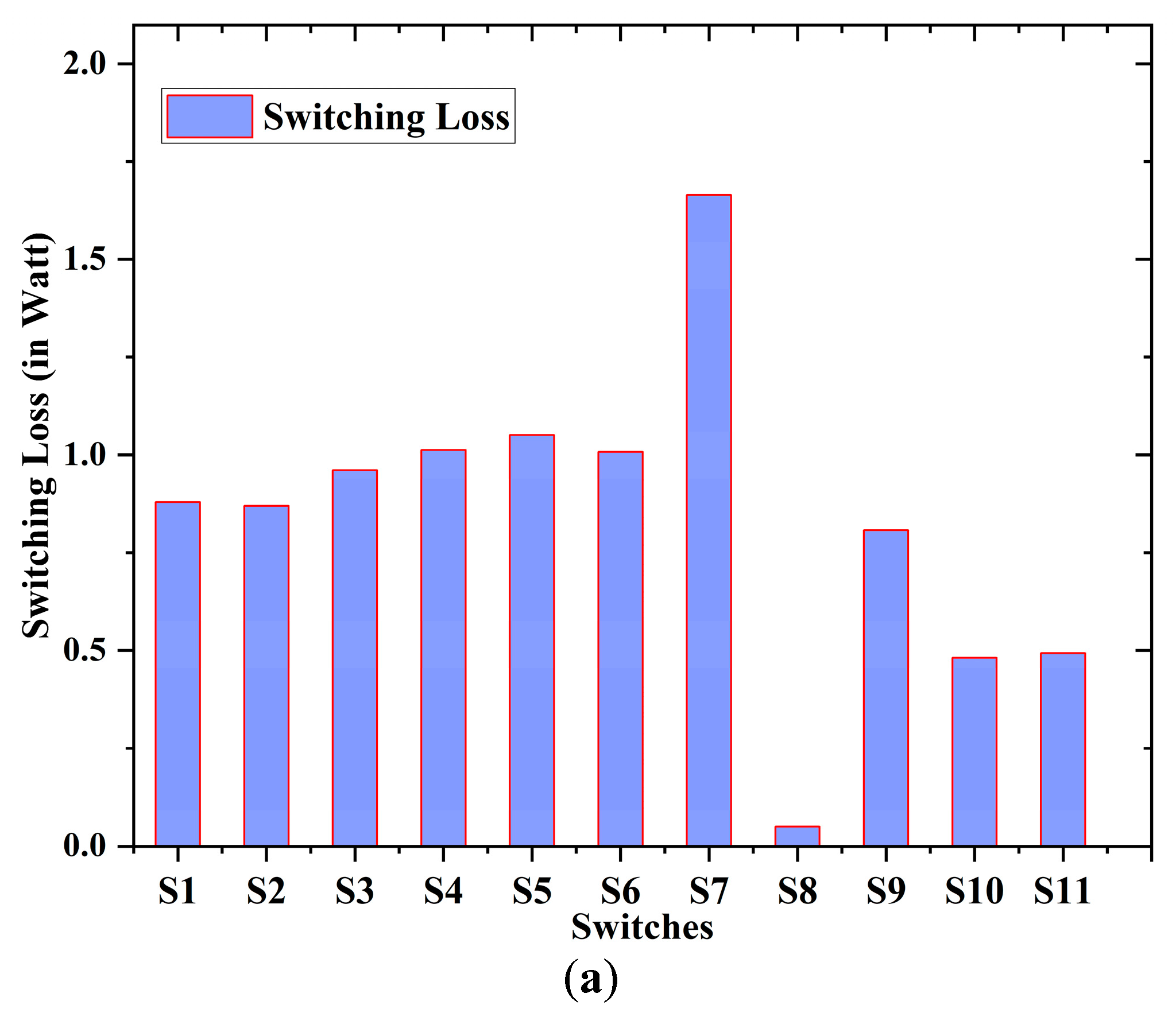
- (a)
- It employs eleven switches and four DC sources to generate a waveform with 25 levels of output voltage.
- (b)
- The proposed MLI does not require an H-bridge for negative polarity generation.
- (c)
- The proposed topology was initially modeled and simulated using the MATLAB/Simulink 2019b platform.
- (d)
- A 25-level inverter is proposed, simulated, and designed in the laboratory. The experimental results validate the smooth operation of the inverter.
- (e)
- Only three switches are conducted to generate any voltage levels.
- (f)
- The staircase waveform enhances power quality and lowers overall total harmonic distortion (THD).
2. Proposed Modular Structure Topology
2.1. Cascaded Operations
2.1.1. Case 1 (For Identical Voltage Ratios in All Modules)
2.1.2. Case 2 (For Voltage Ratio of 52t:52t+1, Where t = p−1 and ‘p’ is the Module)
3. Comparison Study
3.1. Comparison of Inverter Circuits with H-Bridge Configuration [14,15,16,17,18,19,20,21]
3.2. Comparison of Inverter Circuits without H-Bridge Configuration [22,23,24,25,26,27,28,29,30,31,32,33]
4. Simulation and Experimental Studies
5. Conclusions
Author Contributions
Funding
Data Availability Statement
Conflicts of Interest
References
- Chen, M.; Gao, C.; Yin, C.; Loh, P.C. Novel Cascaded Seven-Level Inverter with Embedded Voltage Boosting for Renewable Energy Applications. CPSS Trans. Power Electron. Appl. 2022, 7, 58–70. [Google Scholar] [CrossRef]
- Mondol, H.; Biswas, S.P.; Islam, R.; Mahfuz-Ur-Rahman, A.M.; Muttaqi, K.M. A New Hybrid Multilevel Inverter Topology with Level Shifted Multi-carrier PWM Technique for Harvesting Renewable Energy. In Proceedings of the 2020 IEEE Industry Applications Society Annual Meeting, Detroit, MI, USA, 10–16 October 2020; pp. 2574–2585. [Google Scholar] [CrossRef]
- Reddi, N.K.; Ramteke, M.R.; Suryawanshi, H.M.; Kothapalli, K.; Gawande, S.P. An Isolated Multi-Input ZCS DC–DC Front-End-Converter Based Multilevel Inverter for the Integration of Renewable Energy Sources. IEEE Trans. Ind. Appl. 2018, 54, 494–504. [Google Scholar] [CrossRef]
- Balachandran, A.; Jonsson, T.; Eriksson, L. Design and Analysis of Battery-Integrated Modular Multilevel Converters for Automotive Powertrain Applications. In Proceedings of the 2021 23rd European Conference on Power Electronics and Applications (EPE’21 ECCE Europe), Ghent, Belgium, 6–10 September 2021; pp. 1–12. [Google Scholar] [CrossRef]
- Khoucha, F.; Lagoun, S.M.; Marouani, K.; Kheloui, A.; Benbouzid, M.E.H. Hybrid Cascaded H-Bridge Multilevel-Inverter Induction-Motor-Drive Direct Torque Control for Automotive Applications. IEEE Trans. Ind. Electron. 2010, 57, 892–899. [Google Scholar] [CrossRef]
- Modeer, T.; Pallo, N.; Foulkes, T.; Barth, C.B.; Playa-Podgurski, R.C.N. Design of a GaN-Based Interleaved Nine-Level Flying Capacitor Multilevel Inverter for Electric Aircraft Applications. IEEE Trans. Power Electron. 2020, 35, 12153–12165. [Google Scholar] [CrossRef]
- Mahto, K.K.; Mahato, B.; Chandan, D.; Das, P.; Das, G.; Fotis, M. Mann. A New Symmetrical Source-Based DC/AC Converter with Experimental. Verification. Electron. 2024, 13, 1975. [Google Scholar] [CrossRef]
- Chen, W.L.; Su, Y.H. Negative Sequence Active and Reactive Currents Compensation for Unbalanced Three-Phase Networks Subject to Various Line Impedance Attributes. IEEE J. Emerg. Sel. Top. Power Electron. 2022, 10, 2528–2538. [Google Scholar] [CrossRef]
- Yadav, D.; Singh, N.; Bhadoria, V.; Vita, V.; Fotis, G.; Tsampasis, E.G.; Maris, T.I. Analysis of the Factors Influencing the 300 Performance of Single- and Multi-Diode PV Solar Modules. IEEE Access 2023, 11, 95507–95525. [Google Scholar] [CrossRef]
- Maris, T.I.; Kourtesi, S.; Ekonomou, L.; Fotis, G. Modeling of a single-phase photovoltaic inverter. Sol. Energy Mater. Sol. Cells 2007, 91, 1713–1725. [Google Scholar] [CrossRef]
- Ponnusamy, P.; Sivaraman, P.; Almakhles, D.J.; Padmanaban, S.; Leonowicz, Z.; Alagu, M.; Ali, J.S.M. A New Multilevel Inverter Topology with Reduced Power Components for Domestic Solar PV. Appl. IEEE Access 2020, 8, 187483–187497. [Google Scholar] [CrossRef]
- Bughneda, A.; Salem, M.; Richelli, A.; Ishak, D.; Alatai, S. Review of multilevel inverters for PV energy system applications. Energies 2021, 14, 1585. [Google Scholar] [CrossRef]
- Mahato, B.; Majumdar, S.; Jana, K.C. Carrier-based PWM techniques for multi-level inverters: A comprehensive performance study. Gazi Univ. J. Sci. Part. A Eng. Innov. 2018, 5, 101–111. [Google Scholar]
- Hosseinzadeh, M.A.; Sarebanzadeh, M.; Garcia, C.F.; Babaei, E.; Rodriguez, J.; Kennel, R. Reduced Multisource Switched-Capacitor Multilevel Inverter Topologies. IEEE Trans. Power Electron. 2022, 37, 14647–14666. [Google Scholar] [CrossRef]
- Chamarthi, P.K.; Agarwal, V.; Meutas, M.S.E.; Khadkakar, V. Novel 1–0 Dual Input Nine-Level Inverter Topology with Generalized Modulation Technique. IEEE Trans. Energy Convers. 2022, 37, 1789–1802. [Google Scholar] [CrossRef]
- Sadanala, C.; Pattoaik, S.P.; Singh, V.P. A novel switched capacitor based multilevel inverter with symmetrical and asymmetrical configurations. Electr. Eng. 2021, 103, 1461–1472. [Google Scholar] [CrossRef]
- Darmian, S.Y.; Barakati, S.M. A New Asymmetric Multilevel Inverter with Reduced Number of Components. IEEE J. Emerg. Sel. Top. Power Electron. 2020, 8, 4333–4342. [Google Scholar] [CrossRef]
- Pradeep, J.; Vengadakrishnan, K.; Palani, A.; Sandirasegarane, T. A new tri- source symmetric cascaded multilevel inverter topology with reduced power components. Circuit World 2022, 49, 431–444. [Google Scholar] [CrossRef]
- Chandrasekaran, K.; Mohanty, N.K.; Ranganathan, S. A new tapped sources stack succored modified HX bridge MLI Circuit World. Circuit World 2021, 47, 164–172. [Google Scholar] [CrossRef]
- Mahato, B.; Majumdar, S.; Jana, K.C. A new and generalized MLI with overall lesser power electronic devices. J. Circuits Syst. Comput. 2019, 29, 2050058. [Google Scholar] [CrossRef]
- Paul, S.; Mahato, B.; Majumdar, S.; Jana, K.C. A Novel H-Type MLI with the reduction in Power Electronic Devices. In Proceedings of the 2021 12th Power Electronics, Drive Systems, and Technologies Conference (PEDSTC), Tabriz, Iran, 2–4 February 2021; pp. 1–5. [Google Scholar] [CrossRef]
- Tupakula, R.R. A generalized single-phase cascaded multilevel inverter with reduced switch count. Electr. Eng. 2021, 103, 1115–1125. [Google Scholar] [CrossRef]
- Khasm, S.R.; Dhaminyslu, C. Design and Implementation of Asymmetrical Multilevel Inverter with Reduced Components and Low Voltage Stress. IEEE Access 2022, 10, 3495–3511. [Google Scholar] [CrossRef]
- Babaei, E.; Hosseinzadeh, M.A.; Sarbanzadeh, M.; Cecati, C. A new basic unit for cascaded multilevel inverters with reduced number of power electronic devices. In Proceedings of the 2016 7th Power Electronics and Drive Systems Technologies Conference (PEDSTC), Tehran, Iran, 16–18 February2016; pp. 185–190. [Google Scholar] [CrossRef]
- Harbi, I.A.; Azazi, H.Z.; Lashing, A.E.; Elsabbe, A. A higher levels multilevel inverter with reduced number of switches. Int. J. Electron. 2020, 105, 1286–1299. [Google Scholar] [CrossRef]
- Kannan, C.; Mohanty, N.K. A Non-modular Matrix Structure for Component Count Waning in Multilevel Inversion. Electr. Eng. Technol. 2022, 17, 251–259. [Google Scholar] [CrossRef]
- Mahato, B.; Majumdar, S.; Jana, K.C.; Babaei, E.; Mohanta, D.K. A new switch-diode cell-based single-phase cascaded multilevel inverter. Soft Comput. 2023, 27, 13719–13738. [Google Scholar] [CrossRef]
- Mahato, B.; Majumdar, S.; Paul, S.; Pal, P.K.; Jana, K.C. A new and modular back-to-back connected T-type inverter for minimum number of power devices, TSV, and cost factor. IETE Tech. Rev. 2022, 39, 357–374. [Google Scholar] [CrossRef]
- Mahato, B.; Ranjan, M.; Pal, P.K.; Gupta, S.K.; Mahto, K.M. Design, development and verification of a new multilevel inverter for reduced power switches. Arch. Electr. Eng. 2022, 1051–1063. [Google Scholar] [CrossRef]
- Mahato, B.; Majumdar, S.; Jana, K.C.; Thakura, P.R.; Mohanta, D.K. Experimental verification of a new scheme of MLI based on modified T-type inverter and switched-diode cell with lower number of circuit devices. Electr. Power Compon. Syst. 2021, 48, 1814–1834. [Google Scholar] [CrossRef]
- Mahato, B.; Majumdar, S.; Jana, K.C. Reduction of power electronic devices in a single-phase generalized multilevel inverter. J. Circuits Syst. Comput. 2020, 2050093. [Google Scholar] [CrossRef]
- Majumdar, S.; Mahato, B.; Jana, K.C. Optimum structure-based multi-level inverter with doubling circuit configuration. J. Circuits Syst. Comput. 2019, 1950194. [Google Scholar] [CrossRef]
- Chandrasekaran, K.; Mohanty, N.K. A Flexible Rung Ladder Structured Multilevel Inverter. Tech. Gaz. 2020, 27, 1044–1049. [Google Scholar] [CrossRef]


| Modes | State | T1 | T2 | T3 | T4 | T5 | T6 | T7 | T8 | T9 | T10 | T11 | State | Modes |
|---|---|---|---|---|---|---|---|---|---|---|---|---|---|---|
| 1 | +1 Vdc | ✔ | ✖ | ✖ | ✖ | ✔ | ✔ | −1 Vdc | 14 | |||||
| 2 | +2 Vdc | ✔ | ✖ | ✖ | ✔ | ✖ | ✔ | −2 Vdc | 15 | |||||
| 3 | +3 Vdc | ✖ | ✔ | ✔✖ | ✔ | ✖ | −3 Vdc | 16 | ||||||
| 4 | +4 Vdc | ✔ | ✔ | ✖ | ✔ | ✖ | ✖ | −4 Vdc | 17 | |||||
| 5 | +5 Vdc | ✖ | ✔ | ✖ | ✔ | ✔✖ | −5 Vdc | 18 | ||||||
| 6 | +6 Vdc | ✖ | ✔ | ✔✖ | ✔✖ | −6 Vdc | 19 | |||||||
| 7 | +7 Vdc | ✔ | ✖ | ✖ | ✔ | ✔✖ | −7 Vdc | 20 | ||||||
| 8 | +8 Vdc | ✖ | ✔ | ✔ | ✖ | ✔ | ✖ | −8 Vdc | 21 | |||||
| 9 | +9 Vdc | ✔ | ✖ | ✔✖ | ✔ | ✖ | −9 Vdc | 22 | ||||||
| 10 | +10 Vdc | ✖ | ✔ | ✖ | ✔ | ✔ | ✖ | −10 Vdc | 23 | |||||
| 11 | +11 Vdc | ✖ | ✔ | ✔ | ✔✖ | −11 Vdc | 24 | |||||||
| 12 | +12 Vdc | ✔ | ✖ | ✖ | ✔ | ✔ | ✖ | −12 Vdc | 25 | |||||
| 13 | 0 | ✔✖ | ✔✖ | ✔✖ | 0 | 13 |
| Switches | T7 | T1, T2 | T9 | T8 | T5, T6 | T3, T4, T10, T11 |
|---|---|---|---|---|---|---|
| TSV *(Vdc) | 1 | 2 | 5 | 6 | 10 | 12 |
| No. of Module | Voltage Levels (NL) | IGBTs (NS) | Diodes (Nd) | Gate Drivers (Ng) | DC Sources (Ndc) |
|---|---|---|---|---|---|
| 1 | 25 | 16 | 16 | 11 | 4 |
| 2 | 49 | 32 | 32 | 22 | 8 |
| 3 | 73 | 48 | 48 | 33 | 12 |
| ︙ | ︙ | ︙ | ︙ | ︙ | ︙ |
| p | (24p + 1) | 16p | 16p | 11p | 4p |
| No. of Module | Voltage Levels (NL) | IGBTs (NS) | Diodes (Nd) | Gate Drivers (Ng) | DC Sources (Ndc) |
|---|---|---|---|---|---|
| 1 | 25 | 16 | 16 | 11 | 4 |
| 2 | 625 | 32 | 32 | 22 | 8 |
| 3 | 15,625 | 48 | 48 | 33 | 12 |
| ︙ | ︙ | ︙ | ︙ | ︙ | ︙ |
| p | 25p | 16p | 16p | 11p | 4p |
| Module 1 | Module 2 | Module 3 |
|---|---|---|
| V1L = 5 Vdc V1R = Vdc Output voltage levels: 0, ±1 Vdc, ±2 Vdc, ±3 Vdc, ±4 Vdc, ±5 Vdc, ±6 Vdc, ±7 Vdc, ±8 Vdc, ±9 Vdc, ±10 Vdc, ±11 Vdc, ±12 Vdc | V2L = 5 Vdc V2R = Vdc Output voltage levels: 0, ±1 Vdc, ±2 Vdc, ±3 Vdc, ±4 Vdc, ±5 Vdc, ±6 Vdc, ±7 Vdc, ±8 Vdc, ±9 Vdc, ±10 Vdc, ±11 Vdc, ±12 Vdc | V3L = 5 Vdc V3R = Vdc Output voltage levels: 0, ±1 Vdc, ±2 Vdc, ±3 Vdc, ±4 Vdc, ±5 Vdc, ±6 Vdc, ±7 Vdc, ±8 Vdc, ±9 Vdc, ±10 Vdc, ±11 Vdc, ±12 Vdc |
| Module-1 | Module-2 | Module-3 |
|---|---|---|
| V1L = 5 Vdc V1R = Vdc Output voltage levels: 0, ±1 Vdc, ±2 Vdc, ±3 Vdc, ±4 Vdc, ±5 Vdc, ±6 Vdc, ±7 Vdc, ±8 Vdc, ±9 Vdc, ±10 Vdc, ±11 Vdc, ±12 Vdc | V2L = 125 Vdc V2R = 25 Vdc Output voltage levels: 0, ±25 Vdc, ±50 Vdc, ±75 Vdc, ±100 Vdc, ±125 Vdc, ±150 Vdc, ±175 Vdc, ±200 Vdc, ±225 Vdc, ±250 Vdc, ±275 Vdc, ±312 Vdc | V3L = 3125 Vdc V3R = 625 Vdc Output voltage levels: 0, ±625 Vdc, ±1250 Vdc, ±1875 Vdc, ±2500 Vdc, ±3125 Vdc, ±3750 Vdc, ±4375 Vdc, ±5000 Vdc, ±5625 Vdc, ±6250 Vdc, ±6875 Vdc, ±7500 Vdc |
| Parameters | Case 1 | Case 2 |
|---|---|---|
| Voltage levels | (24p + 1) | 25p |
| Power switches | 16p | 16p |
| DC sources | 4p | 4p |
| m2 | −12 | −11 | −10 | −9 | −8 | . . . . | 0 | . . . . | 8 | 9 | 10 | 11 | 12 | |
|---|---|---|---|---|---|---|---|---|---|---|---|---|---|---|
| m1 | ||||||||||||||
| −12 | −24 | −23 | −22 | −21 | −20 | . . . . | −12 | . . . . | −4 | −3 | −2 | −1 | 0 | |
| −11 | −23 | −22 | −21 | −20 | −19 | . . . . | −11 | . . . . | −3 | −2 | −1 | 0 | 1 | |
| −10 | −22 | −21 | −20 | −19 | −18 | . . . . | −10 | . . . . | −2 | −1 | 0 | 1 | 2 | |
| −9 | −21 | −20 | −19 | −18 | −17 | . . . . | −9 | . . . . | −1 | 0 | 1 | 2 | 3 | |
| −8 | −20 | −19 | −18 | 17 | −16 | . . . . | −8 | . . . . | 0 | 1 | 2 | 3 | 4 | |
| ︙ | ︙ | ︙ | ︙ | ︙ | ︙ | ︙ | ︙ | ︙ | ︙ | ︙ | ︙ | |||
| 0 | −12 | −11 | −10 | −9 | −8 | . . . . | 0 | . . . . | 8 | 9 | 10 | 11 | 12 | |
| ︙ | ︙ | ︙ | ︙ | ︙ | ︙ | ︙ | ︙ | ︙ | ︙ | ︙ | ︙ | ︙ | ︙ | |
| 8 | −4 | −3 | −2 | −1 | 0 | . . . . | 8 | . . . . | 16 | 17 | 18 | 19 | 20 | |
| 9 | −3 | −2 | −3 | 0 | 1 | . . . . | 9 | . . . . | 17 | 18 | 19 | 20 | 21 | |
| 10 | −2 | −1 | 0 | 1 | 2 | . . . . | 10 | . . . . | 18 | 19 | 20 | 21 | 22 | |
| 11 | −1 | 0 | 1 | 2 | 3 | . . . . | 11 | . . . . | 19 | 20 | 21 | 22 | 23 | |
| 12 | 0 | 1 | 2 | 3 | 4 | . . . . | 12 | . . . . | 20 | 21 | 22 | 23 | 24 | |
| m2 | −300 | −275 | −250 | −225 | −200 | . . . . | 0 | . . . . | 200 | 225 | 250 | 275 | 300 | |
|---|---|---|---|---|---|---|---|---|---|---|---|---|---|---|
| m1 | ||||||||||||||
| −12 | −312 | −287 | −262 | −237 | −212 | . . . . | −12 | . . . . | 192 | 213 | 238 | 263 | 288 | |
| −11 | −311 | −286 | −261 | −236 | −211 | . . . . | −11 | . . . . | 191 | 214 | 239 | 262 | 289 | |
| −10 | −310 | −285 | −260 | −235 | −210 | . . . . | −10 | . . . . | 190 | 215 | 240 | 261 | 290 | |
| −9 | −309 | −284 | −259 | −234 | −209 | . . . . | −9 | . . . . | 189 | 216 | 241 | 260 | 291 | |
| −8 | −308 | −283 | −258 | −233 | −208 | . . . . | −8 | . . . . | 188 | 217 | 241 | 259 | 292 | |
| ︙ | ︙ | ︙ | ︙ | ︙ | ︙ | ︙ | ︙ | ︙ | ︙ | ︙ | ︙ | ︙ | ||
| 0 | −300 | −275 | −250 | −225 | −200 | . . . . | 0 | . . . . | 200 | 225 | 250 | 275 | 300 | |
| ︙ | ︙ | ︙ | ︙ | ︙ | ︙ | ︙ | ︙ | ︙ | ︙ | ︙ | ︙ | ︙ | ||
| 8 | −292 | −267 | −242 | −217 | −192 | . . . . | 8 | . . . . | 208 | 233 | 258 | 283 | 308 | |
| 9 | −291 | −266 | −241 | −216 | −191 | . . . . | 9 | . . . . | 209 | 234 | 259 | 284 | 309 | |
| 10 | −290 | −265 | −240 | −215 | −190 | . . . . | 10 | . . . . | 210 | 235 | 260 | 285 | 310 | |
| 11 | −289 | −264 | −239 | −214 | −189 | . . . . | 11 | . . . . | 211 | 236 | 261 | 286 | 311 | |
| 12 | −288 | −263 | −238 | −213 | −188 | . . . . | 12 | . . . . | 212 | 237 | 262 | 287 | 312 | |
| Type of Topology | Reference No. | Total Switches | Gate Drivers | DC Sources | No. of Voltage Levels | Switches in Current Conduction Path |
|---|---|---|---|---|---|---|
| Topologies with H-bridges | [14] | 16 | 16 | 2 | 33 | 6 |
| [15] | 7 | 7 | 2 | 9 | 3 | |
| [16] | 14 | 14 | 2 | 21 | 4 | |
| [17] | 13 | 13 | 5 | 49 | 2 | |
| [18] | 12 | 12 | 3 | 7 | 5 | |
| [19] | 11 | 11 | 3 | 7 | 3 | |
| [20] | 9 | 9 | 3 | 9 | 5 | |
| [21] | 9 | 9 | 4 | 17 | 3 | |
| Topologies without H-bridges | [22] | 3 | 3 | 3 | 15 | 5 |
| [23] | 12 | 12 | 4 | 33 | 6 | |
| [24] | 12 | 12 | 5 | 27 | 4 | |
| [25] | 8 | 8 | 4 | 9 | 6 | |
| [26] | 8 | 8 | 2 | 9 | 4 | |
| [27] | 9 | 9 | 2 | 9 | 4 | |
| [28] | 10 | 10 | 3 | 7 | 4 | |
| [29] | 11 | 11 | 5 | 27 | 4 | |
| [30] | 8 | 8 | 4 | 15 | 4 | |
| [31] | 6 | 6 | 4 | 9 | 3 | |
| [32] | 6 | 6 | 3 | 7 | 3 | |
| [33] | 7 | 7 | 3 | 15 | 4 | |
| Proposed | 11 | 11 | 4 | 25 | 3 |
| Parameters | Specification | |
|---|---|---|
| Switching parameters for IGBT | CT-60AM-18F: 900 V, 60 A Von, IGBT = 1.3 V, Von, Dio = 1.5 V, RDio = 0.01 Ω, RIGBT = 0.11 Ω, β = 3 | |
| Types of switching devices and their controlling elements | Driver Controller | TLP250: 10–35 V, ±1.5 A DS1103 |
| Simulation and experimental parameters for V1 = V2 = 25 V, V3 = V4 = 125 V | R = 180 Ω, L = 25 mH, Vpk = 259.2 V, Ipk = 1.2 A, MI = 0.8. | |
| R = 180 Ω, L = 150 mH, Vpk = 259.2 V, Ipk = 0.9 A, MI = 0.8. | ||
| R = 180 Ω, L = 25 mH, Vpk = 301 V, Ipk = 1.3 A, MI = 1. | ||
Disclaimer/Publisher’s Note: The statements, opinions and data contained in all publications are solely those of the individual author(s) and contributor(s) and not of MDPI and/or the editor(s). MDPI and/or the editor(s) disclaim responsibility for any injury to people or property resulting from any ideas, methods, instructions or products referred to in the content. |
© 2024 by the authors. Licensee MDPI, Basel, Switzerland. This article is an open access article distributed under the terms and conditions of the Creative Commons Attribution (CC BY) license (https://creativecommons.org/licenses/by/4.0/).
Share and Cite
Das, D.; Mahato, B.; Chandan, B.; Joshi, H.; Mahto, K.K.; Das, P.; Fotis, G.; Vita, V.; Mann, M. A New Cascaded Multilevel Inverter for Modular Structure and Reduced Passive Components. Electronics 2024, 13, 3566. https://doi.org/10.3390/electronics13173566
Das D, Mahato B, Chandan B, Joshi H, Mahto KK, Das P, Fotis G, Vita V, Mann M. A New Cascaded Multilevel Inverter for Modular Structure and Reduced Passive Components. Electronics. 2024; 13(17):3566. https://doi.org/10.3390/electronics13173566
Chicago/Turabian StyleDas, Durbanjali, Bidyut Mahato, Bikramaditya Chandan, Hitesh Joshi, Kailash Kumar Mahto, Priyanath Das, Georgios Fotis, Vasiliki Vita, and Michael Mann. 2024. "A New Cascaded Multilevel Inverter for Modular Structure and Reduced Passive Components" Electronics 13, no. 17: 3566. https://doi.org/10.3390/electronics13173566