
Smart Transfer Planer with Multiple Antenna Arrays to Enhance Low Earth Orbit Satellite Communication Ground Links


Abstract
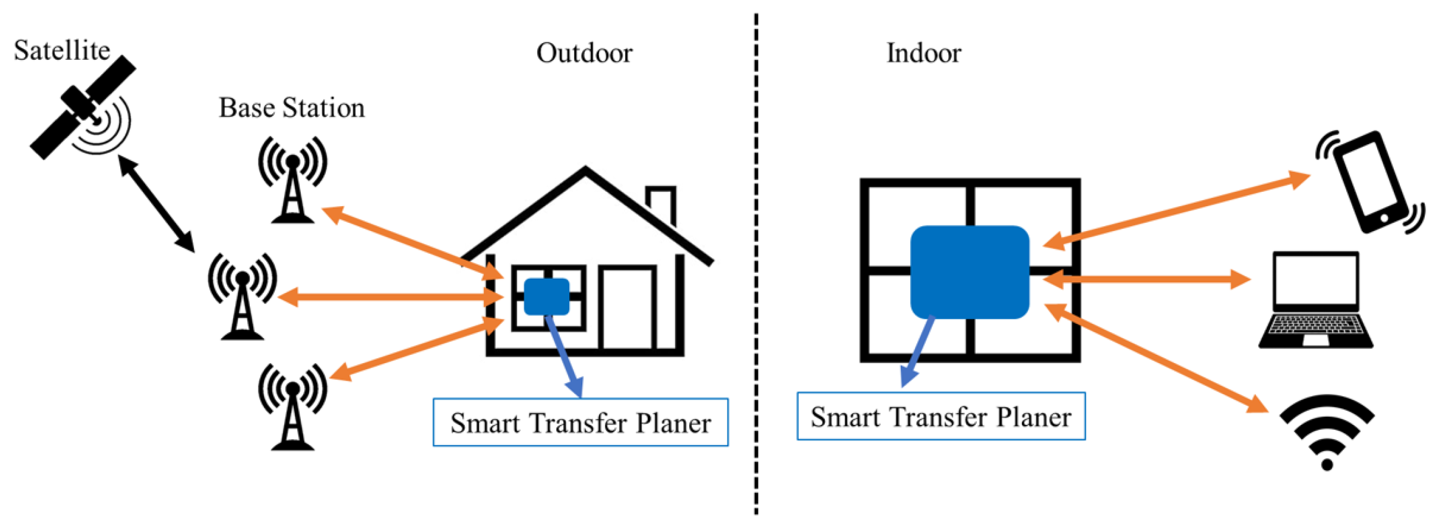
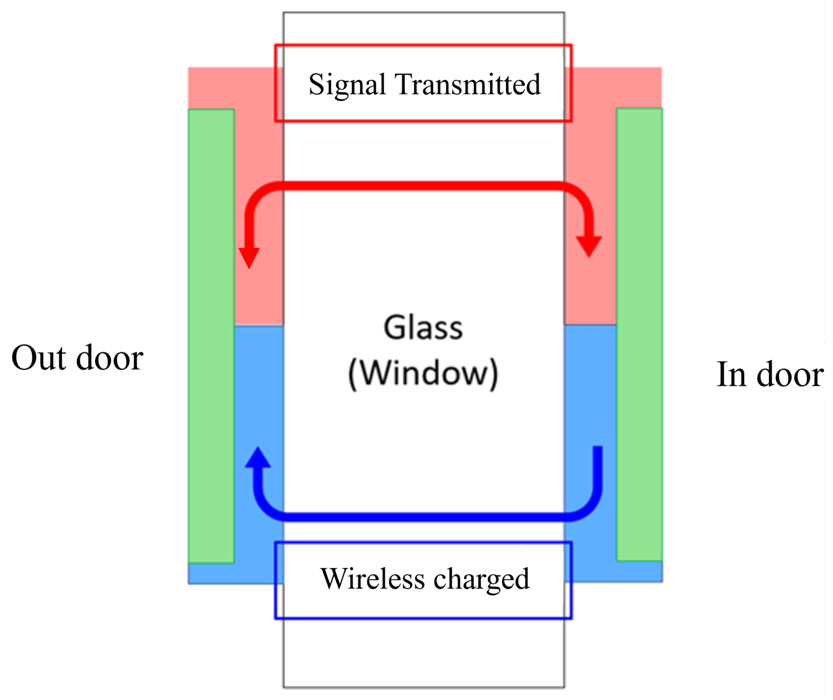
:1. Introduction
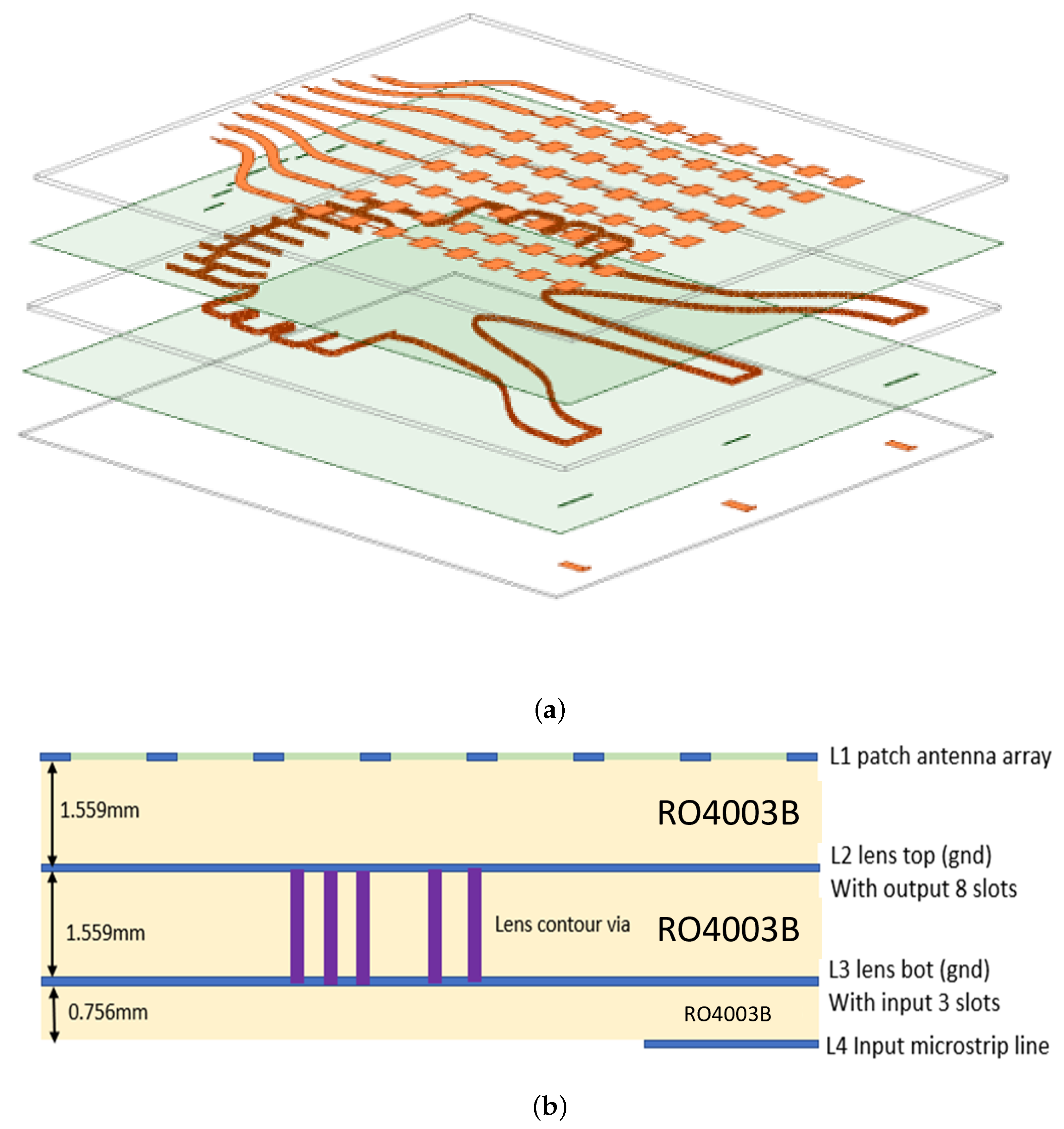
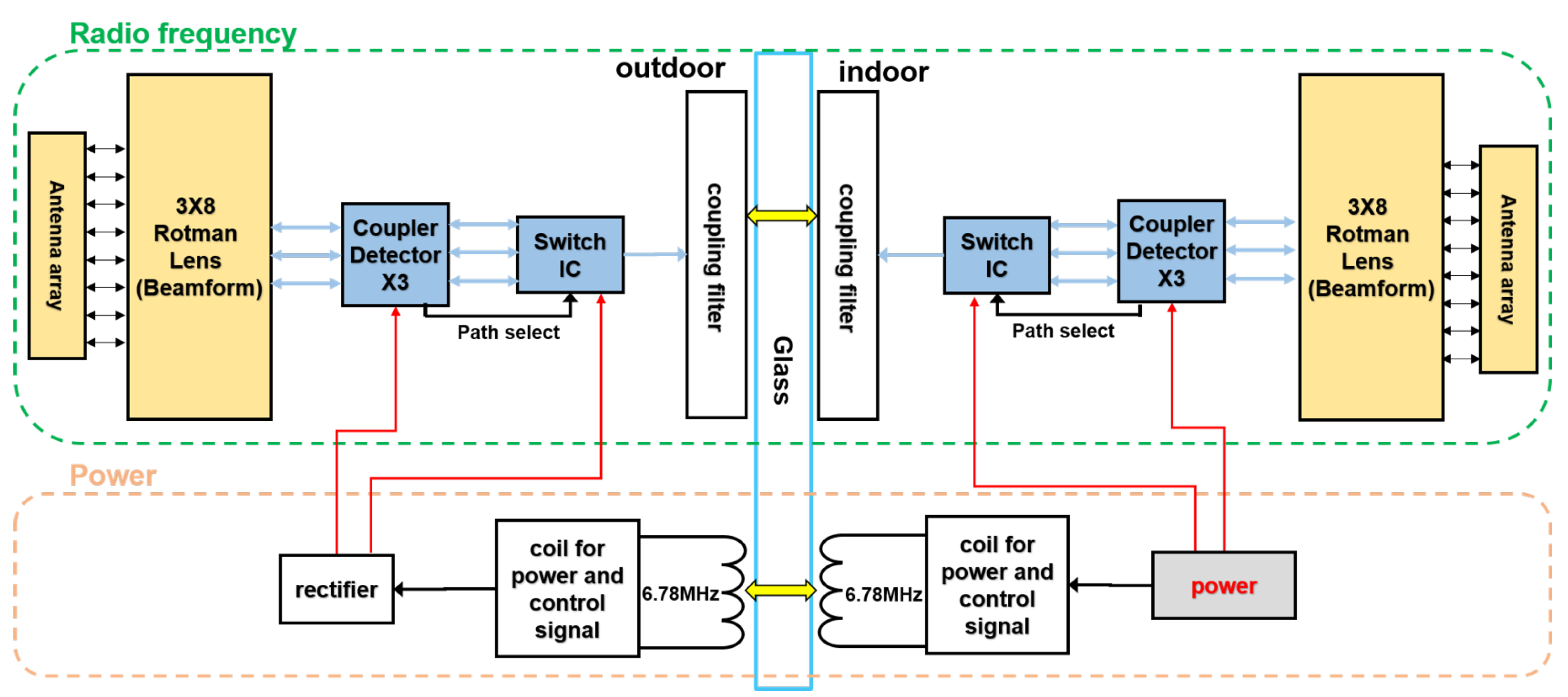
2. Design Concept of Smart Transfer Planer
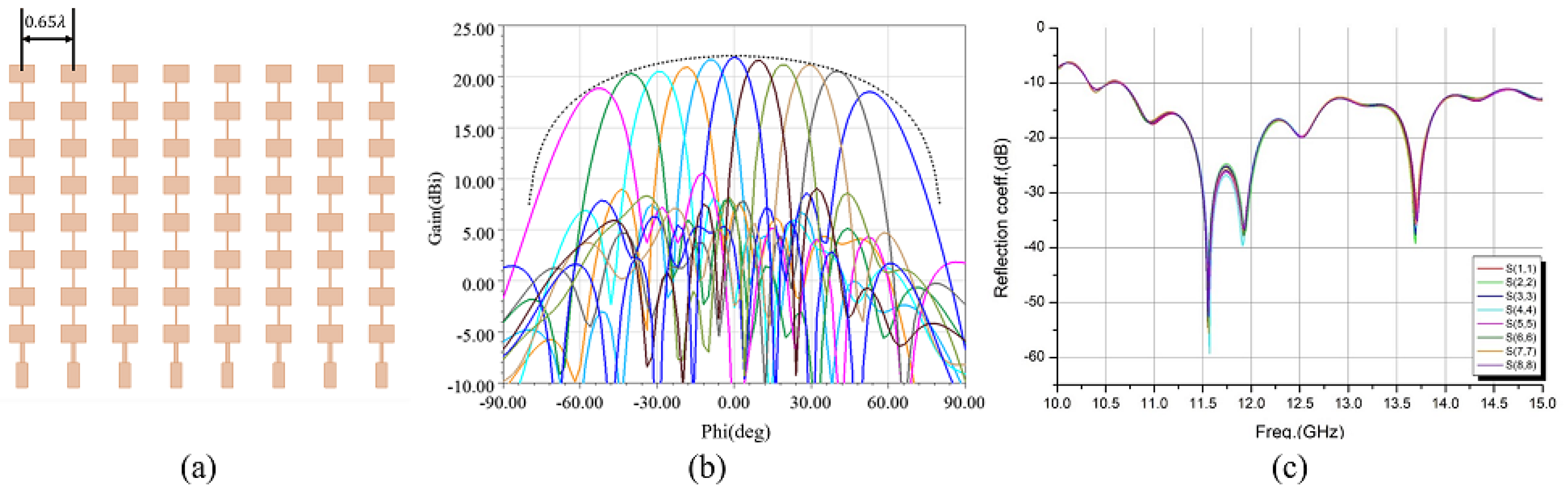
2.1. Antenna Array
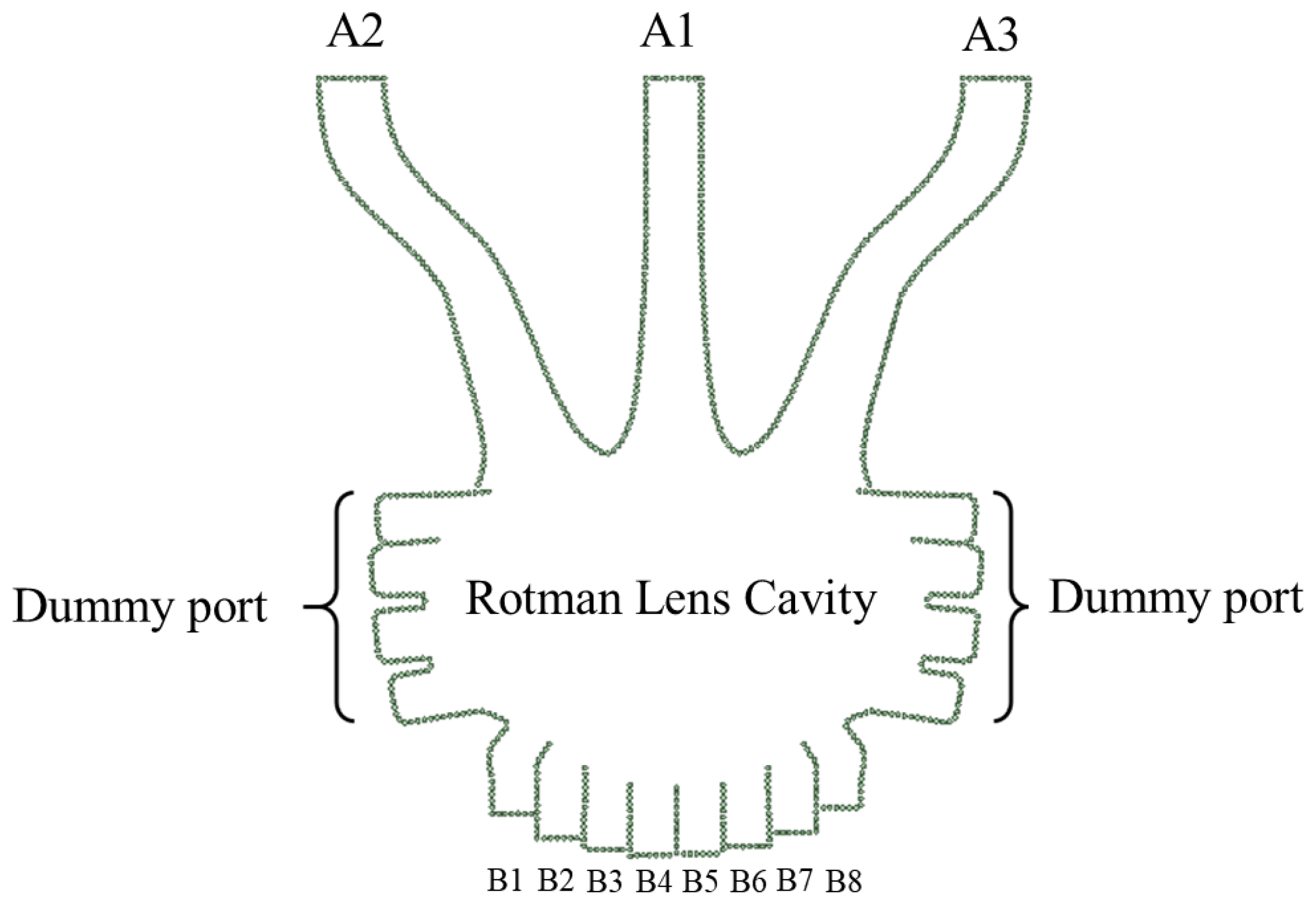
2.2. Beamforming Network
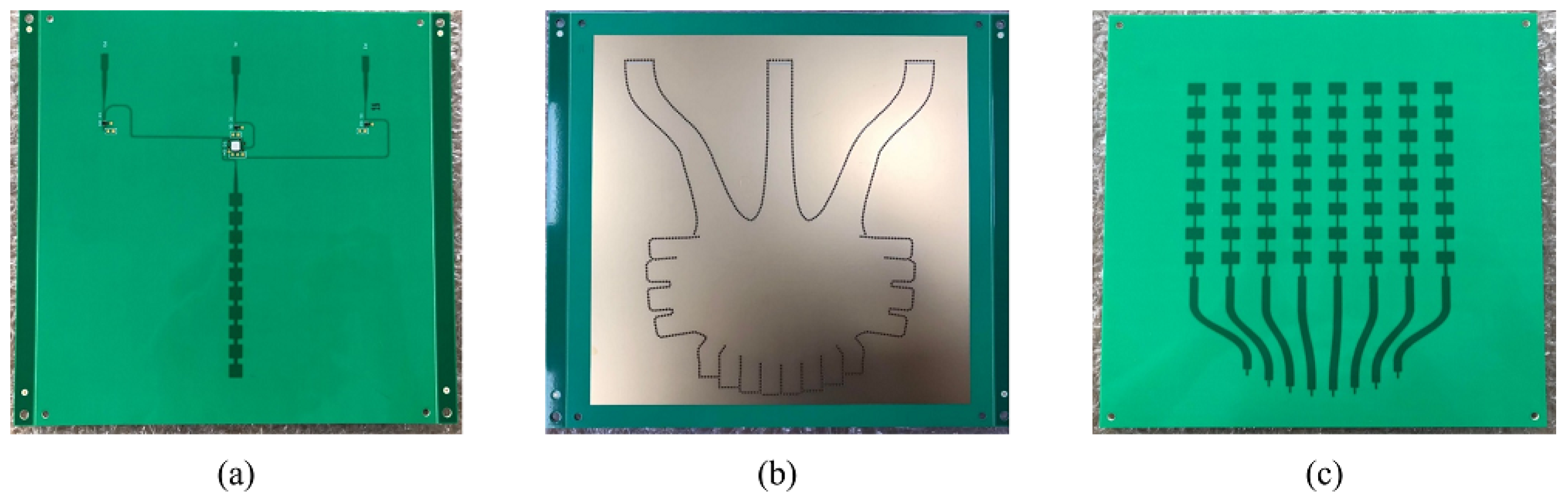
2.3. Smart Transfer Planer Fabrication
2.4. Signal Transform
2.5. Switch Circuit
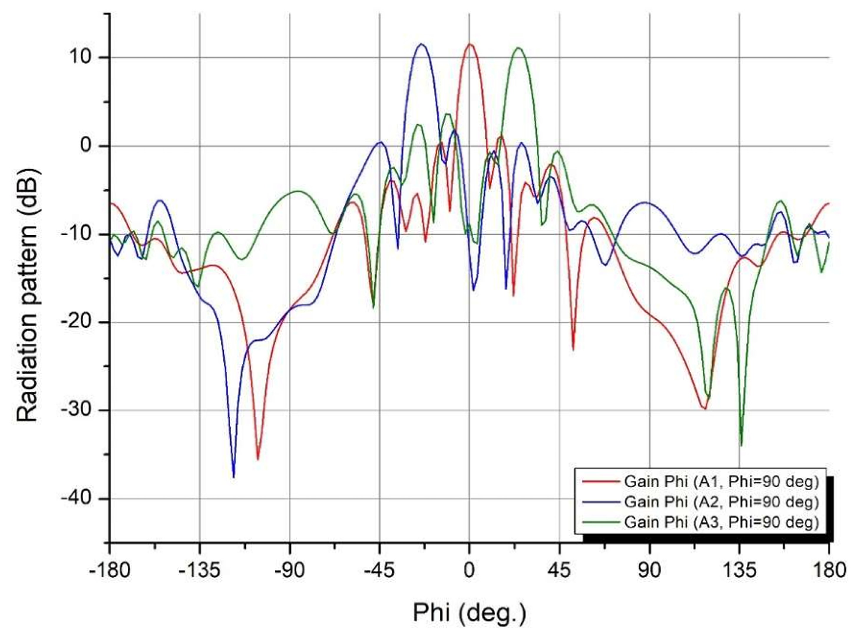
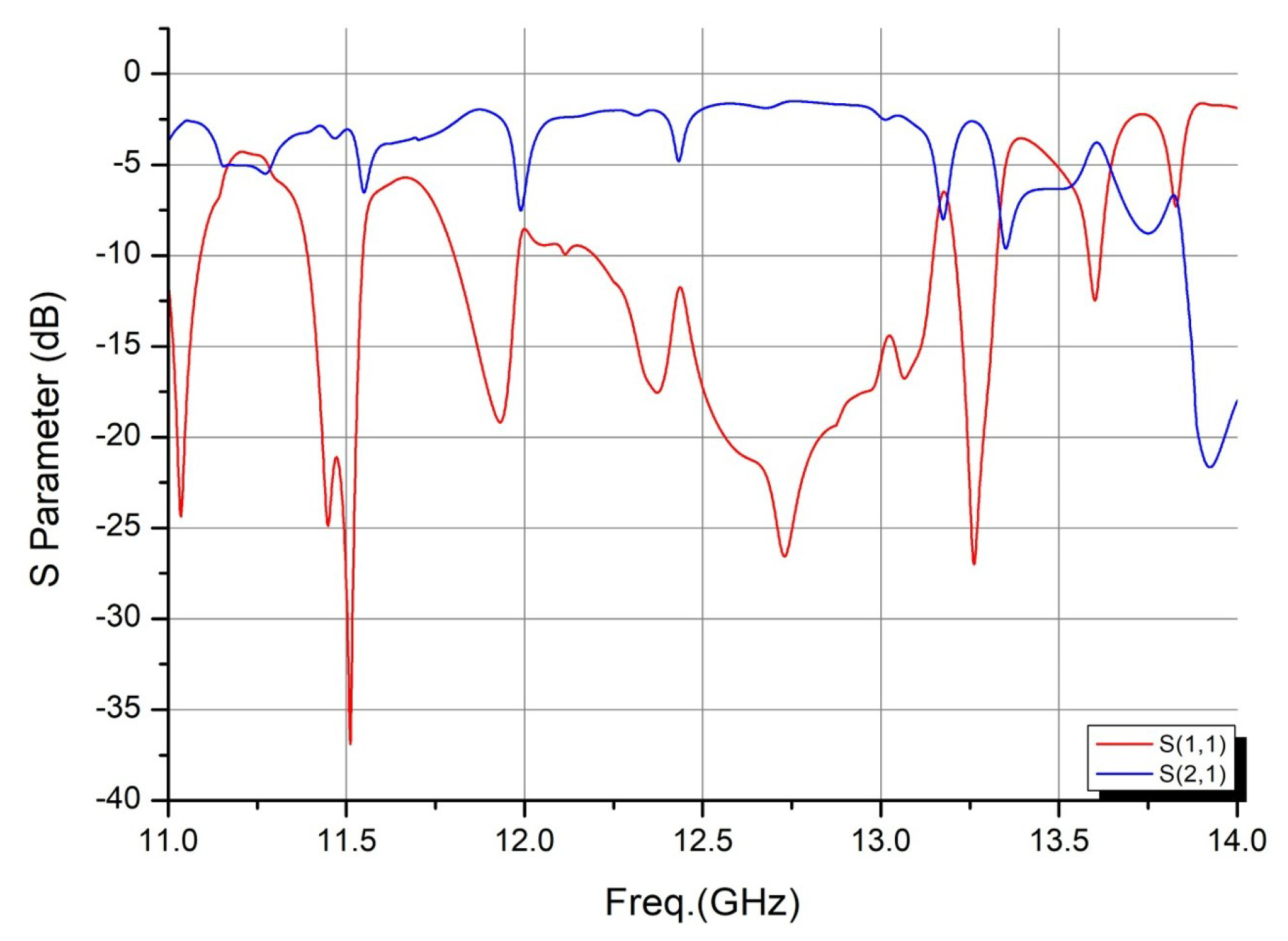
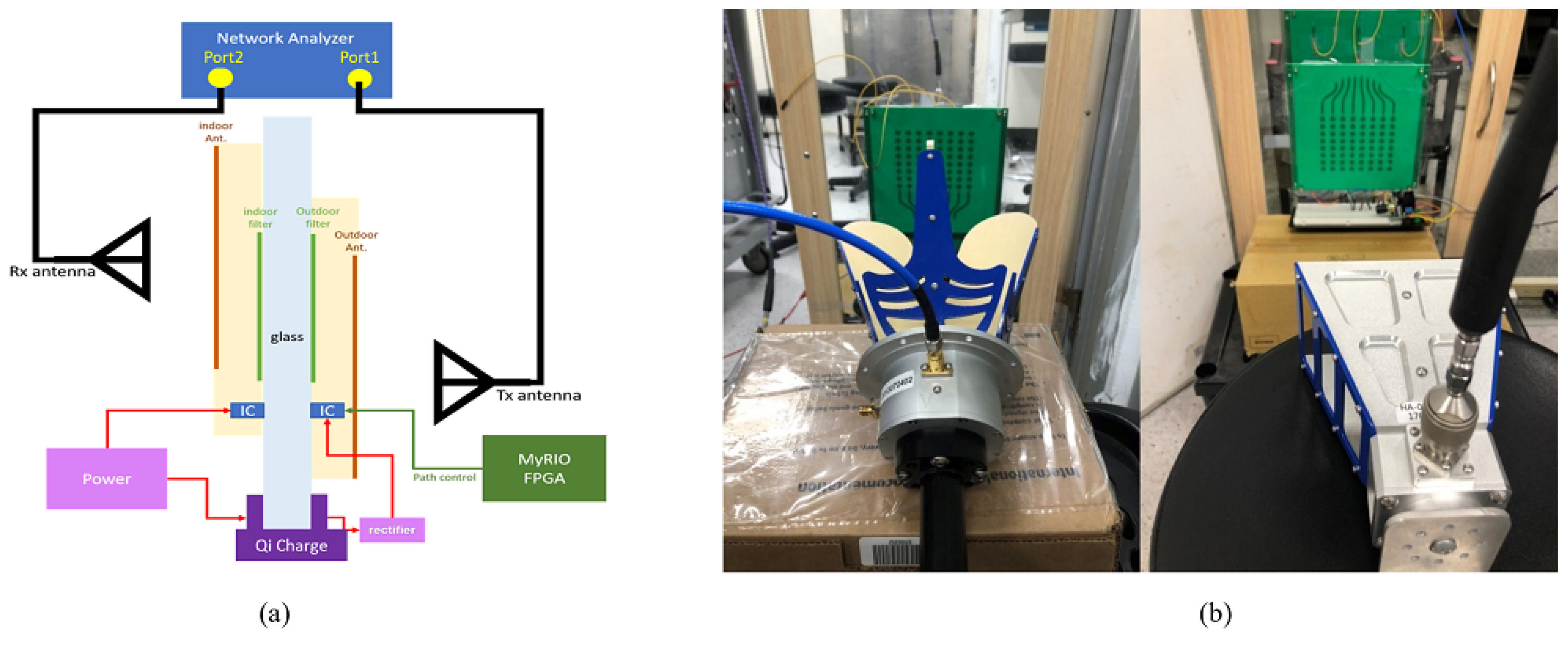
3. Experimental Results
4. Conclusions
Author Contributions
Funding
Data Availability Statement
Conflicts of Interest
References
- Chang, M.-L.; Lin, D.-B.; Rao, H.-T.; Lin, H.-Y.; Chou, H.-T. Smart Transfer planer for Enhancing Low Earth Orbit Satellite Communication Ground Links. In Proceedings of the 2023 Asia-Pacific Microwave Conference (APMC), Taipei, Taiwan, 5–8 December 2023; p. 143. [Google Scholar] [CrossRef]
- Stutzman, W.L.; Thiele, G.A. Antenna Theory and Design, 3rd ed.; John Wiley & Sons Inc.: Hoboken, NJ, USA, 1998. [Google Scholar]
- Babas, D.G.; Sahalos, J.N. Synthesis method of series-fed microstrip antenna arrays. Electron. Lett. 2007, 43, 78–80. [Google Scholar] [CrossRef]
- Mydhili, K.; Parvathi, P.; Prasanthi, K. Design and simulation of edge fed microstrip patch antenna array. In Proceedings of the 2018 2nd International Conference on I-SMAC (IoT in Social, Mobile, Analytics and Cloud) (I-SMAC), Palladam, India, 30–31 August 2018; pp. 356–360. [Google Scholar] [CrossRef]
- Liu, D.; Gu, X.; Baks, C.W.; Valdes-Garcia, A. Antenna-in-Package Design Considerations for Ka-Band 5G Communication Applications. IEEE Trans. Antennas Propag. 2017, 65, 6372–6379. [Google Scholar] [CrossRef]
- Rotman, W.; Turner, R. Wide-angle microwave lens for line source applications. IEEE Trans. Antennas Propag. 1963, 11, 623–632. [Google Scholar] [CrossRef]
- Rajabalian, M.; Zakeri, B. An implemented non-focal Rotman Lens. In Proceedings of the 2015 European Radar Conference (EuRAD), Paris, France, 9–11 September 2015; pp. 393–396. [Google Scholar] [CrossRef]
- Adibifard, S. Design of Wideband Rotman Lenses with Dummy Ports for Wide-Scan Phased Array Applications. Master’s Thesis, Ecole de Technologie Superieure Universite du Quebec, Montréal, QC, Canada, 2016. [Google Scholar]
- Chou, C.-H.; Ho, S.-K.; Lin, D.-B.; Chou, H.-T. Beam Switchable Antenna Array Design by Rotman Lens with SIW Feeding Lines for Vehicular Applications. In Proceedings of the 2021 International Symposium on Antennas and Propagation (ISAP), Taipei, Taiwan, 19–21 October 2021; pp. 1–2. [Google Scholar] [CrossRef]
- Du, J.K.; So, K.; Ra, Y.; Jung, S.Y.; Kim, J.; Kim, S.Y.; Woo, S.; Kim, H.-T.; Ho, Y.-C.; Paik, W. Dual-polarized patch array antenna package for 5G communication systems. In Proceedings of the 2017 11th European Conference on Antennas and Propagation (EUCAP), Paris, France, 19–24 March 2017; pp. 3493–3496. [Google Scholar] [CrossRef]
- Omar, A.A.; Dib, N.I. Analysis of slot-coupled transitions from microstrip to-microstrip and microstrip-to-waveguides. IEEE Trans. Microw. Theory Tech. 1997, 45, 1127–1132. [Google Scholar] [CrossRef]
- Chen, Z.; Wu, X.; Yang, F. A compact SIW butler matrix with straight delay lines at 60 GHz. In Proceedings of the 2017 IEEE International Symposium on Antennas and Propagation & USNC/URSI National Radio Science Meeting, San Diego, CA, USA, 9–14 July 2017; pp. 2141–2142. [Google Scholar]
- Huang, X.; Wu, K. A Broadband U-Slot Coupled Microstrip-to-Waveguide Transition. IEEE Trans. Microw. Theory Tech. 2012, 60, 1210–1217. [Google Scholar] [CrossRef]
- Molaei, B.; Khaleghi, A. A NovelWideband Microstrip Line to Ridge GapWaveguide Transition Using Defected Ground Slot. IEEE Microw. Wirel. Compon. Lett. 2015, 25, 91–93. [Google Scholar] [CrossRef]
- Tu, W.-H.; Chang, K. Compact microstrip bandstop filter using open stub and spurline. IEEE Microw. Wireless Compon. Lett. 2005, 15, 268–270. [Google Scholar]
- Lee, W.; Kim, J.; Yoon, Y.J. Compact Two-Layer Rotman Lens-Fed Microstrip Antenna Array at 24 GHz. IEEE Trans. Antennas Propag. 2011, 59, 460–466. [Google Scholar] [CrossRef]
- Pozar, D.M. Microwave Engineering, Revised ed.; Wiley: New York, NY, USA, 2005. [Google Scholar]
- Sbarra, E.; Marcaccioli, L.; Gatti, R.V.; Sorrentino, R. A novel rotman lens in SIW technology. In Proceedings of the 2007 European Radar Conference, Munich, Germany, 10–12 October 2007; pp. 236–239. [Google Scholar] [CrossRef]


| Receiver Angle | |||
|---|---|---|---|
| Received power without STP (dB) | −52.2 | −53.9 | 50.6 |
| Received power with STP (dB) | −43.7 | −40 | −40.2 |
| Increased received power (dB) | 9.1 | 10.1 | 10.4 |
Disclaimer/Publisher’s Note: The statements, opinions and data contained in all publications are solely those of the individual author(s) and contributor(s) and not of MDPI and/or the editor(s). MDPI and/or the editor(s) disclaim responsibility for any injury to people or property resulting from any ideas, methods, instructions or products referred to in the content. |
© 2024 by the authors. Licensee MDPI, Basel, Switzerland. This article is an open access article distributed under the terms and conditions of the Creative Commons Attribution (CC BY) license (https://creativecommons.org/licenses/by/4.0/).
Share and Cite
Chang, M.-L.; Lin, D.-B.; Rao, H.-T.; Lin, H.-Y.; Chou, H.-T. Smart Transfer Planer with Multiple Antenna Arrays to Enhance Low Earth Orbit Satellite Communication Ground Links. Electronics 2024, 13, 3581. https://doi.org/10.3390/electronics13173581
Chang M-L, Lin D-B, Rao H-T, Lin H-Y, Chou H-T. Smart Transfer Planer with Multiple Antenna Arrays to Enhance Low Earth Orbit Satellite Communication Ground Links. Electronics. 2024; 13(17):3581. https://doi.org/10.3390/electronics13173581
Chicago/Turabian StyleChang, Mon-Li, Ding-Bing Lin, Hui-Tzu Rao, Hsuan-Yu Lin, and Hsi-Tseng Chou. 2024. "Smart Transfer Planer with Multiple Antenna Arrays to Enhance Low Earth Orbit Satellite Communication Ground Links" Electronics 13, no. 17: 3581. https://doi.org/10.3390/electronics13173581