Article

Novel Power-Efficient Fast-Locking Phase-Locked Loop Based on Adaptive Time-to-Digital Converter-Aided Acceleration Compensation Technology

College of Information Engineering, Henan University of Science and Technology, Luoyang 471023, China
*
Author to whom correspondence should be addressed.
Electronics 2024, 13(18), 3586; https://doi.org/10.3390/electronics13183586
Submission received: 14 August 2024 / Revised: 5 September 2024 / Accepted: 6 September 2024 / Published: 10 September 2024
(This article belongs to the Section Circuit and Signal Processing)

Abstract

:
This paper proposes an adaptive acceleration lock compensation technology for phase-locked loops (PLLs) based on a novel dual-mode programmable ring voltage-controlled oscillator (ring-VCO). In addition, a time-to-digital converter (TDC) is designed to accurately quantify the phase difference from the phase frequency detector (PFD) in order to optimize the dead-zone effect while dynamically switching an auxiliary charge pump (CP) module to realize fast phase locking. Furthermore, a TDC-controlled three/five-stage dual-mode adaptively continuously switched VCO is proposed to optimize the phase noise (PN) and power efficiency, leading to an optimal performance tradeoff of the PLL. Based on the 180 nm/1.8 V standard CMOS technology, the complete PLL design and a corresponding simulation analysis are implemented. The results show that, with a 1 GHz reference signal as the input, the output frequency is 50–324 MHz, with a wide tuning range of 260 MHz and a low phase noise of −98.07 dBc/Hz@1 MHz. The key phase-locking time is reduced to 1.11 μs, and the power dissipation is lowered to 1.86 mW with a layout area of 66 μm × 128 μm. A significantly remarkable multiobjective performance tradeoff with topology optimization is realized, which is in contrast to several similar design cases of PLLs.

1. Introduction

A phase-locked loop (PLL) is a vital component in all electronic communication systems, which have functions related to clock signal generation, frequency synthesis, and data recovery [1,2,3,4,5]. Compared with traditional PLLs, a charge pump phase-locked loop (CP-PLL) provides a highly robust electronic system with a stable reference frequency source. A high-quality PLL circuit has significant advantages such as high speed, low noise, low jitter, low power consumption, low spurious, and easy integration [6,7,8], and it can be widely integrated with various types of clocks—asynchronous/synchronous logical electronic systems. In addition, compared with analogue CP-PLLs, all-digital phase-locked loops (ADPLLs) have advantages in price, locking speed, anti-interference performance, power consumption, and chip area [9,10,11], but the noise feature and spurious performance parameters are not as good as those of the CP-PLLs. Among these aforementioned performance metrics of a PLL circuit, the locking speed and power consumption can be considered as the two core performance parameters [12,13,14,15,16]. With the constraint of optimizing the locking speed of PLLs, achieving the best design tradeoff regarding electrical features between phase noise or jitter and power consumption is currently a challenging research hotspot [17,18]. Therefore, the focus of the PLL design in this study is to implement a more ideal circuit with better comprehensive performance by combining the advantages of two PLLs—CP-PLL and ADPLL circuits.
To address the locking time issue in high-speed, high-frequency PLLs, a study in the literature [19] proposed an effective design scheme based on phase difference cancellation technology to improve locking speed. However, the inability to optimize the dead-zone effect of the phase frequency detectors will still adversely affect the stability of the output frequency of a PLL system. Another study in the literature [20] proposed a design scheme to enhance the output of a charging/discharging current by adding an auxiliary CP module to accelerate the locking phase of the PLLs. However, the added CP modules would result in an unnecessary parallel charging/discharging operation and cause unexpected jitter or noise in the PLL system, and the increased design complexity, power consumption, and circuit area are also some important factors affecting design efficiency.
This paper proposes a novel PLL acceleration locking compensation technology based on an adaptive programmable control technique and aided by a customized time-to-digital converter (TDC), which effectively realizes synchronous tuning and dynamic control in the key submodules of the PFD, CP, and VCO to optimize the locking time and the accuracy of phase frequency detection and to minimize the loss of power consumption while stabilizing the system by restraining jitter and phase noise. The detailed contributions of this study are summarized as follows:
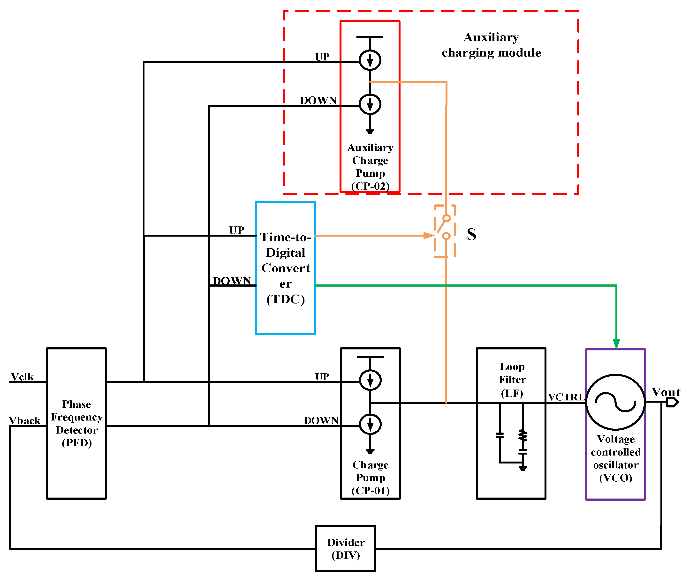
  • An aided TDC circuit is implemented as the core adaptive control module in the PLL, and it can accurately convert the phase difference signal to switch the instructions to dynamically control the CP and VCO.
  • An auxiliary secondary CP with a selectable switch is designed to construct a parallel output topology that forms paired CP modules, which can double the charging/discharging current to speed up the locking phase; otherwise, the CP operates in power-saving mode.
  • A novel coarse- or fine-grained programmable frequency tunable ring voltage-controlled oscillator (VCO) is proposed, which can be adaptively tuned to the third or the fifth order by the TDC in order to dynamically optimize the phase noise and power consumption, leading to an optimal performance tradeoff.
The remainder of this paper is organized as follows: Section 2 gives a general introduction to the proposed novel PLL architecture. Section 3 presents the details of the PLL design tradeoff and introduces the circuit design and operation principles of the TDC-controlled CPs and ring-VCOs. Section 4 demonstrates the Cadence-based pre/post-layout simulation results, a comparative analysis, and the discussion. The conclusion and future work are provided in Section 5.

2. PLL Design and Implementation
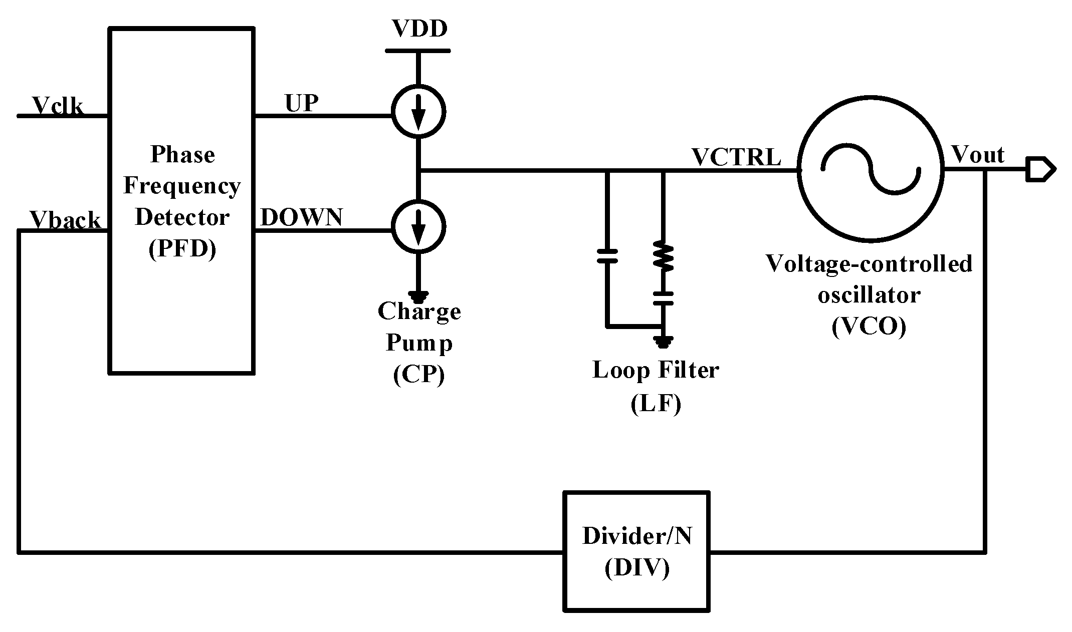
2.1. Previous Work

The traditional topology of a PLL circuit is shown in Figure 1 [21], consisting of the following five functional submodules: a phase frequency detector (PFD), a charge pump (CP), a loop filter (LF, generally using a low-pass filter), a voltage-controlled oscillator (VCO), and a frequency divider (DIV). The main operating principle is as follows: The phase difference between the input reference and feedback signal of the DIV in the PFD is calculated. Then, the obtained phase difference is converted into a voltage signal by the CP and LF, and this signal is used to drive and continuously adaptively adjust the output frequency of the VCO. Finally, the phase-locking function is activated until the phase difference between the input reference and the feedback signal becomes zero.
For the mainstream design of a PLL circuit, having achieved the expected output frequency, determining how to comprehensively optimize the design tradeoff in terms of the locking time, phase jitter and noise, power consumption, and circuit area is the core task of designers. The locking time directly determines the operating efficiency of the microelectronic communication system, and the remarkable noise-processing feature with an acceptable power efficiency directly determines the transmission quality, reliability, and applicability of the communication system. In the PLL system, phase noise is mainly caused by white noise and 1/f noise sources in the high-speed switching operation of the internal active MOS transistor devices [22,23].

2.2. Proposed PLL Architecture

The fast-locking compensation circuit topology of the PLL proposed in this study is shown in Figure 2. Compared with Figure 1, two auxiliary functional modules are added, a time-to-digital converter (TDC) and a secondary CP are designed, and the TDC is a core control module in this novel PLL architecture.
As illustrated in the connection diagram in Figure 2, first, the phase difference between the two system input signals is detected by the PFD and then converted into a digital control signal by the TDC. Then, this control signal is sent to turn on switch S and connect the outputs of the two sets of CP modules together in parallel so that the total output charging/discharging current of the CPs can be doubled to drive the subsequent LPF and VCO more powerfully in order to speed up the locking time of the PLL. At the same time, the voltage-controlled ring oscillator is adaptively switched into the third or fifth order according to whether the level of the control signal from the TDC is high or low. Furthermore, by combining the controls with Vctrl, the output frequency is dynamically adjusted to continuously reduce the phase difference until it is under the threshold value, and the PLL completes the phase-locking function. Finally, once locking is achieved, the TDC outputs a low-level signal to turn off the double-current switch S, and then the secondary auxiliary CP module stops working and enters power-saving mode for power efficiency. Therefore, the overall proposed PLL architecture achieves a remarkably significant performance tradeoff in output frequency, operating speed, phase noise, and power consumption.

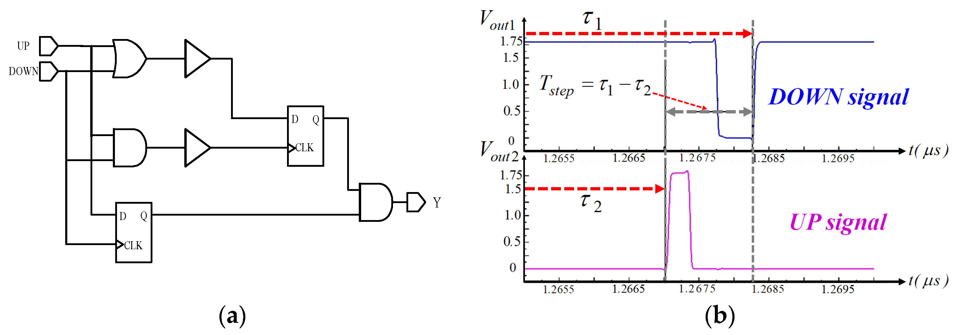
2.3. TDC-Aided Control

As a core functional module in the PLL, the TDC circuit is designed and operated based on a basic differential delay line architecture [24]. As illustrated in Figure 3a, the proposed TDC is composed of the following two delay lines: one is the transmission path of the UP signal, labeled with a time delay of τ2, and the other is the transmission path of the DOWN signal, labeled with a time delay of τ1. When the UP signal arrives before the DOWN signal, the phase difference (the difference value between two delay signals) is considered positive, and vice versa. Regarding the difference value between the two delay lines, as the smallest unit in the phase difference, i.e., the measurable accuracy that can be detected by the TDC, it is generally termed Tstep, which is used to represent the detection resolution of a TDC. As shown in Formula (1), Tstep can be simply calculated as the difference value of τ1 and τ2. Meanwhile, as shown in Figure 3b, in this study, when the output phase difference Tstep falls within 1.25 ns, due to the limitations in detectable accuracy, the TDC will approximate this phase difference value as 0; therefore, the overall PLL system is considered to have completed the phase-locking operation.
T s t e p = τ 1 τ 2

3. Design Tradeoff of Fast-Locking and Other Features

3.1. Theoretical Analysis of Phase Locking

In general, the locking time of the PLL is determined by the closed-loop transfer function of the system, which is expressed in Formula (2) as follows:
H c l o s e ( s ) = K P K v c o R ( s + w z ) s 2 + s K P K v c o R N + w 2 n ; w n = K p K v c o N C ; δ = R 2 K p K v c o C N ;
where wn represents the natural frequency of the closed-loop system of the PLL; δ represents the damping coefficient; and wz represents the zero frequency, i.e., the frequency that makes the numerator of the transfer function be zero. The common approach used to reduce the locking time is to increase the natural frequency wn by reducing the capacitance value of loop capacitor C. KP represents the transfer function of the PFD and the CP current, and Kvco is the tuning gain of the VCO [19]. However, a decrease in the main capacitor value in the filter will cause the noise characteristics of the PLL system to deteriorate, resulting in a contradictory relationship between the two core metrics of the locking time and noise features. In contrast, simply expanding the value of loop capacitor C causes the damping factor to be too large, and the overall PLL system would be in an over-damped state and operate in a non-oscillating discharge process. At the same time, using too many passive components also increases the layout area and product costs of chips.
The output current Icp of the CP determines the locking speed of the PLL. The larger the charge and discharge current Icp, the shorter the delay time and the faster the locking speed is realized. Hence, this study proposes a fast-locking scheme with a doubly enhancing charging/discharging current by adding a secondary auxiliary CP module, as shown in Figure 2.
By only increasing the natural frequency wn and doubling the current Icp, the locking time of the PLL system is effectively reduced, and the damping coefficient and dynamic stability of the system are maintained without varying the capacitor. Finally, once the UP or DOWN value of the output phase difference of the PFD is less than the minimum resolution of the Tstep of the TDC, the PLL circuit achieves and completes phase locking.

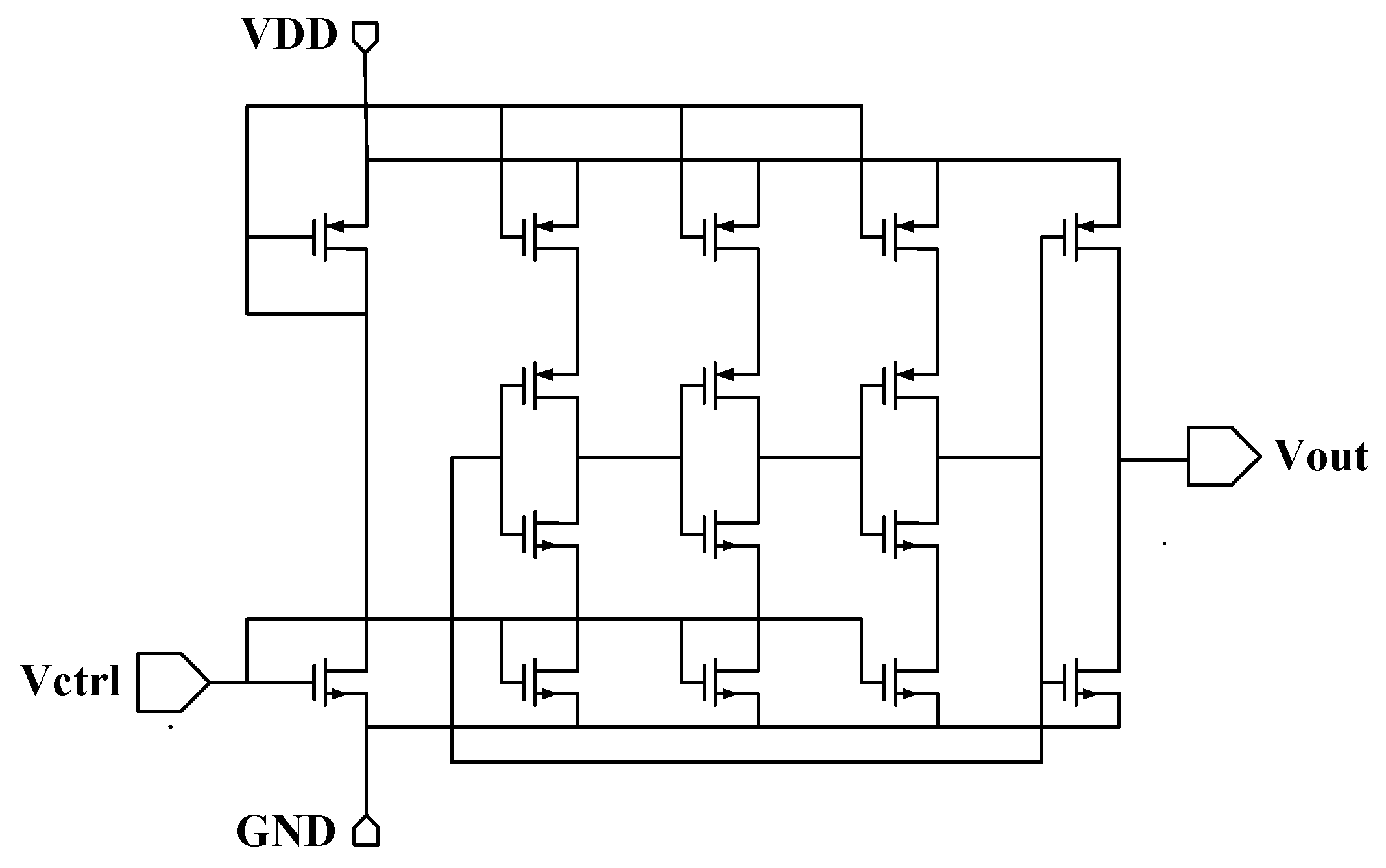
3.2. Principle and Design of Ring-VCO

As the other core module in the PLLs, compared with an LC-type VCO, which has disadvantages in circuit area due to a large passive inductor and capacitor, large power consumption, and poor anti-radiation ability [25], a ring-type voltage-controlled oscillator (VCO) has obvious advantages in terms of a lower design complexity, good circuit area and power efficiency, and easy programmability and architecture extensibility. Therefore, for an adaptable high- or low-level voltage control of the TDC, as well as considering the output frequency, which should be lower than the GHz level, a ring-VCO with a three/five-stage frequency switchable topology is proposed in this study. A ring-VCO is used because the TDC-based adaptive switching control can counteract and compensate for the negative impacts caused by the fast-locking process of the PLL, such as increased power consumption, jitter, and system instability. Therefore, a three/five-stage ring-VCO can achieve a significant superior performance tradeoff in the proposed PLL with fast-locking, power-saving, and anti-noise features.
Figure 4 shows an example of a conventional three-stage ring-VCO, which is well known as a non-linear feedback system.
According to the Barkhausen criterion, a ring oscillator needs to meet the following two basic conditions in oscillation frequency in order to achieve stable oscillation: the loop gain must be greater than one, and the total phase of the feedback loop must be zero. The total phase is further divided into a DC phase shift and a frequency phase shift, and the DC phase shift of a single-stage inverter is 180°. The phase shift is mainly dependent on the number of poles introduced by the logic inverters in the system, where the stage inverter can only reach 90° under ideal conditions. Meanwhile, a ring oscillator needs to have at least three inverters. In addition, a common calculation formula used to estimate the output frequency of a ring oscillator is as follows:
f o s c = 1 2 N T
where N and T represent the stage number of the ring oscillator and the phase delay of a single-stage inverter, respectively. As described in Formula (3), a higher output center frequency and a wider tuning range can be obtained by selecting a lower stage number or a lower phase delay.

3.3. Feature Analysis of Individual Three-Stage and Five-Stage Ring Oscillators

Based on the 180 nm/1.8 V standard CMOS technology, Cadence-based circuit designs and corresponding feature simulations are implemented for three- and five-order ring oscillators. The tuning frequency range and phase noise features are mainly evaluated via plotted curves.
First, the simulated tuning frequency range of the three-stage ring oscillator is 0.70–3.35 GHz, as shown in Figure 5a, and the typical phase noise at the 1 MHz offset point is −78.13 dBc/Hz@1 MHz, as shown in Figure 5b. However, with a higher power dissipation likely due to the addition of two-stage inverters, the tunable frequency range and phase noise of each inverter can only provide one pole. Therefore, the ring oscillators are all closed-loop feedback loops composed of an odd number of inverters, and the corresponding values of the five-stage ring oscillator are changed to 0.17–2.00 GHz, as shown in Figure 6a, and −86.89 dBc/Hz@1 MHz, as shown in Figure 6b.
Considering Formula (3) and the related simulation results, it can be concluded that the output center frequency of the ring oscillator drops off, along with the added stage number of inverters, and the tuning frequency range becomes narrow, but the phase noise feature is improved and optimized with more power consumption. Hence, when the TDC-controlled auxiliary CP is operated in the fast-locking mode, which may cause an increase in power consumption, jitter, system instability, etc., the design of the ring-VCO in the PLL is an important tradeoff consideration in terms of the power dissipation, phase noise, center frequency, and tuning range. In this study, by regarding the phase noise feature as the first optimization objective, the three-stage ring oscillator is further optimized by iterative sizing designs to finally realize a better phase noise of −98.07 dBc/Hz@1 MHz, as shown in Figure 7.

3.4. Proposed TDC-Control-Based Adaptive Dual-Mode Switchable Ring-VCO

To realize the best performance tradeoff in the locking time, power consumption, and phase noise features when the PLL switches into the fast-locking or normal operating mode, a novel three/five-stage dual-mode switchable ring-VCO is proposed to assist with the implementation of a power-efficient fast-locking PLL. As shown in Figure 8, the operating mode of the ring-VCO is controlled by the S signal directly sent from the TDC; by switching it into the three- or five-stage mode via the selection of a different number of inverters, the VCO can effectively realize optimized performance tradeoff in the locking speed, phase noise, and power features.
For the phase-locking acceleration mechanism, S needs to be turned on in order to switch the oscillator into the five-stage operating phase; this will significantly reduce the output frequency and further result in a longer output period via the frequency divider module in the feedback loop path. This means that the five-stage mode can speed up the process of frequency division to realize the fast phase locking of the whole PLL system. Otherwise, the ring-VCO operates in the three-stage mode, and the PLL system can continuously reduce the phase difference between the input reference signal and the feedback clock signal with a normal frequency division speed.
In addition to accelerating the phase locking, the output frequency of the PLL can be adaptively adjusted by the input control voltage combined with the TDC control signal synchronously; this is the other key applicable function. At the same time, by using the TDC-based high-precision phase error cancellation technology mentioned above, the stability problems caused by the acceleration of the PLL phase-locking process can also be solved [2,19].
In order to further verify the comprehensive performance of the proposed dual-mode ring-VCO, the Figure of Merit (FoM) value is calculated based on a commonly used formula, as shown in Formula (4):
F o M = P N ( Δ f ) 20 log ( f c Δ f ) + 10 log ( P diss 1 m W )
where PNf) is the phase noise at the Δf frequency offset point (the frequency offset point is generally set to 1 MHz), fC is the central oscillation frequency, and Pdiss is the power dissipation. Table 1 lists all the performance metrics and comparison results of the proposed three-stage ring-VCO with/without transistor size tuning (pre- or post-optimization). As shown in the table, the oscillator, after a number of iteratively optimized sizing designs, has an obvious advantage in terms of the FoM value, obtaining a value of −157.06 dBc/Hz compared with −150.41 dBc/Hz obtained by the previous ring oscillator analyzed in Section 3.3. Thus, the proposed ring-VCO module achieves a significant performance tradeoff between the phase noise and power features.

4. Performance Verification and Discussion

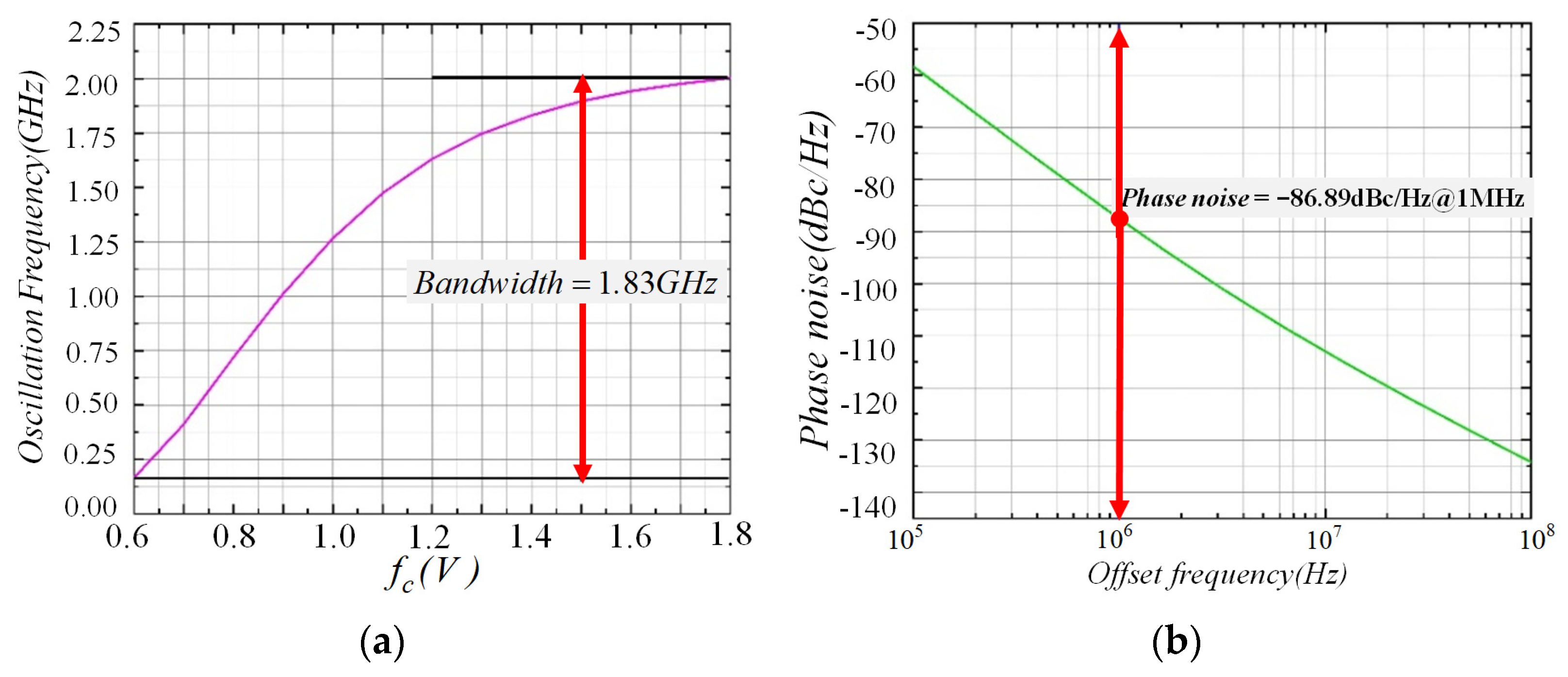
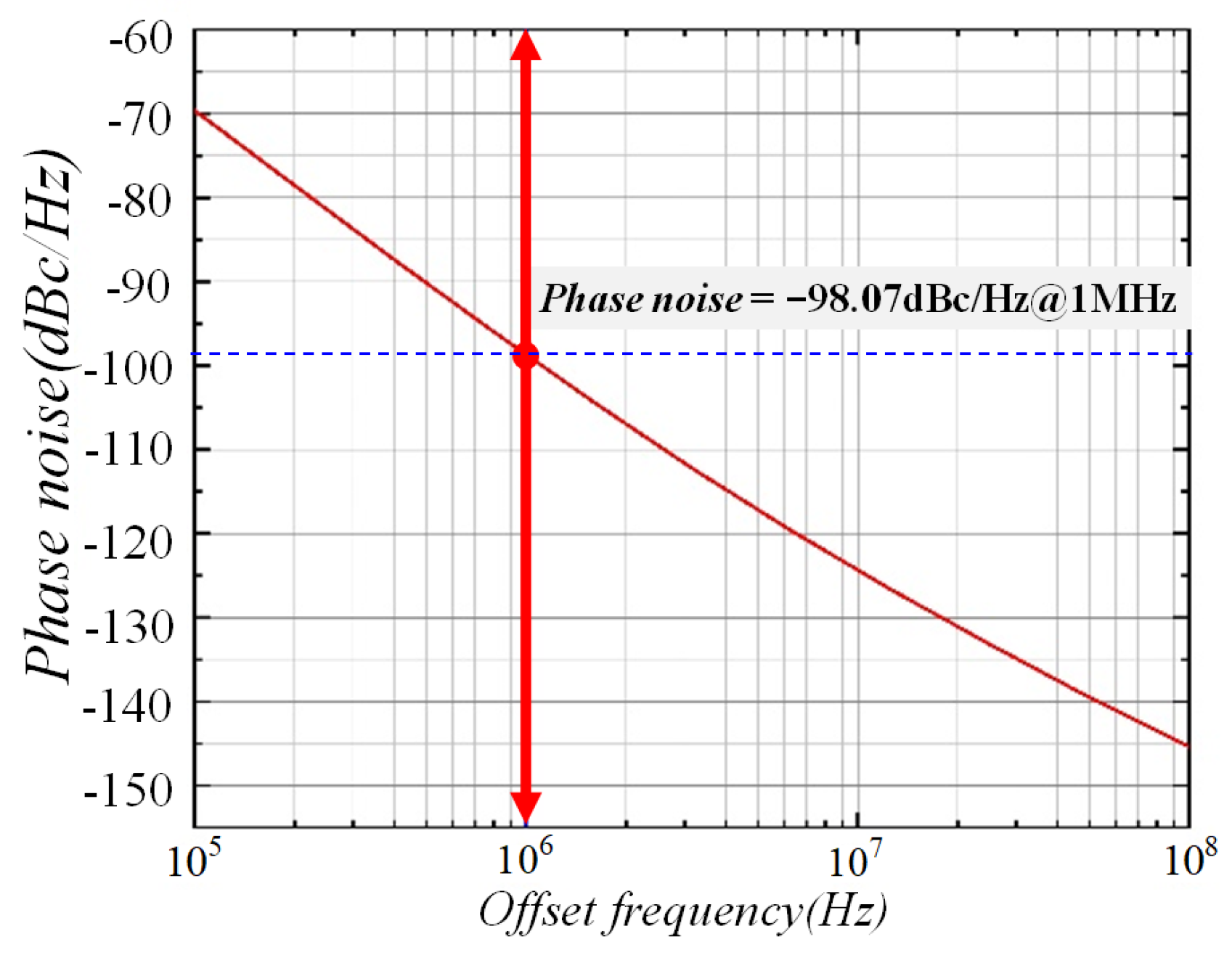
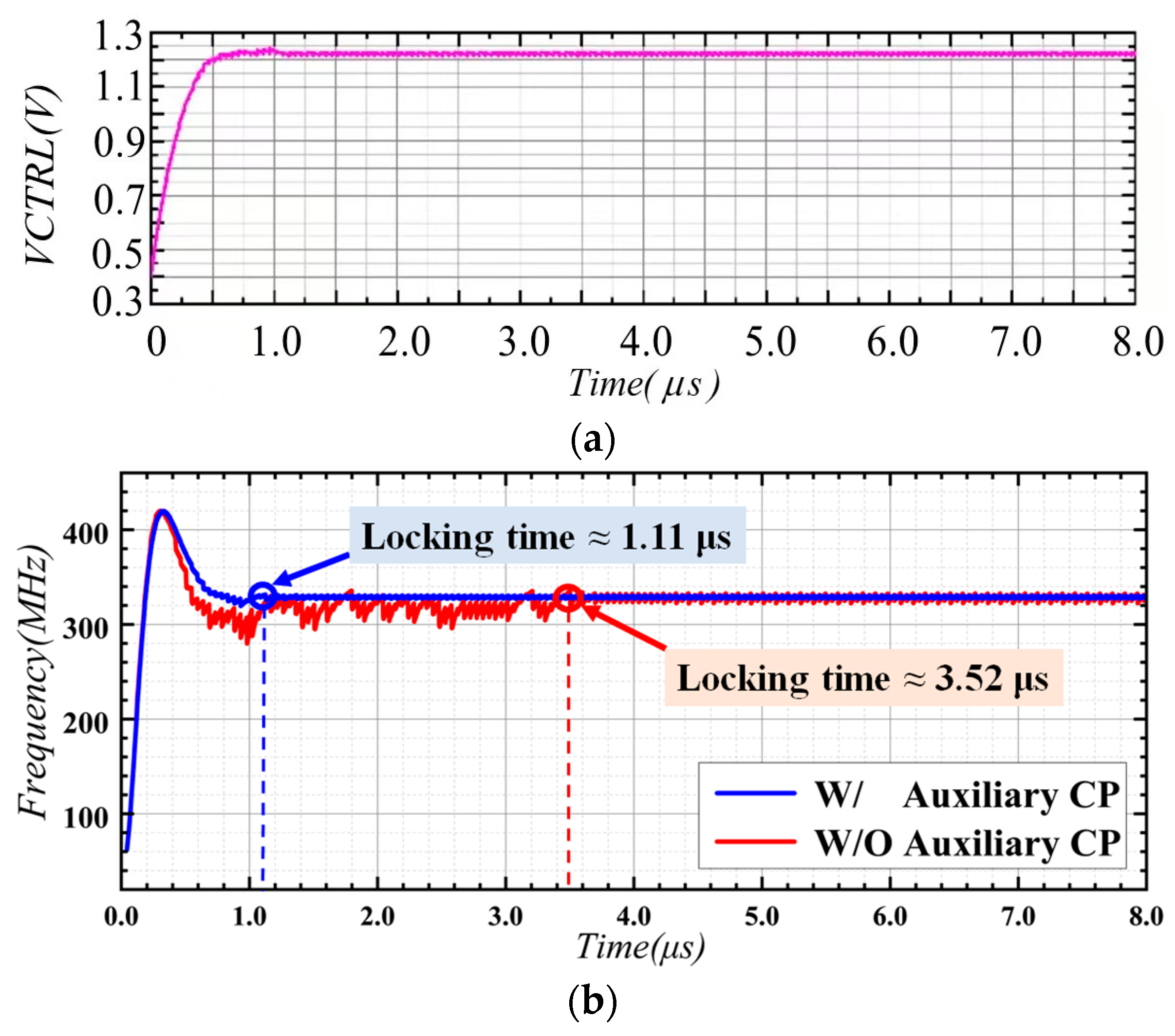
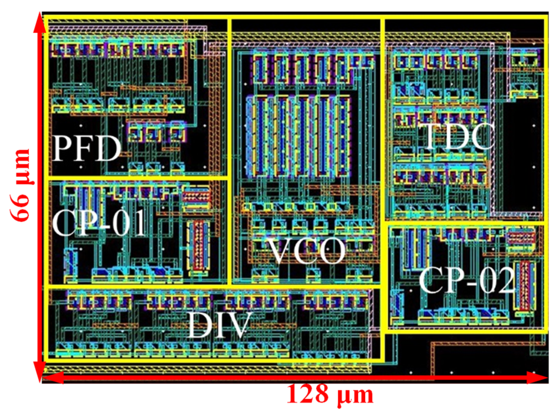
4.1. Simulation-Based Analysis

An all-sided performance evaluation of the proposed fast-locking PLL circuit based on a Cadence simulation is carried out to verify the effectiveness of the core design goals of reducing the locking time while optimizing the phase noise and power consumption features. With a 1 GHz input signal reference at room temperature and an eight-fold frequency divider module in the feedback loop path, the final output frequency of the proposed TDC-aided acceleration PLL is stabilized at 324 MHz. Furthermore, the well-designed PLL has excellent output jitter and phase noise characteristics due to the proposed TDC-aided phase-locked technology. Figure 9 presents the simulation results of the transient noise trend, along with a swept frequency from approximately 0 to 10 GHz, and a sinusoidal noise source is mixed into the power network. The output jitter noise of the overall PLL system can be lowered to 4.92 nV/sqrt (Hz)@1 MHz. Additionally, at a 1.8 V power supply voltage, the average power dissipation is only 1.86 mW, which is extremely low, even in a multi-module complex mixed-signal system. As shown in Figure 10a,b, the most crucial finding of this study is that, with an increase in the control voltage of the core ring-VCO from 0.40 V to 1.22 V, the improved PLL can reach a steady phase-locked state within only 1.11 µs; this locking time is significantly superior to the 3.52 µs required without TDC-controlled fast-locking technology.
The worst case of the proposed PLL is further investigated, and Table 2 exhibits the performance metrics, which are simulated based on different PVT condition corners. Under the process corner in “FF”, with a 10% variation in the power supply voltage of 1.98 V and extremely low temperature conditions of −40 °C, the PLL can realize the shortest phase-locking time of only 0.57 μs, but the power efficiency is worse, increasing to 3.43 mW. Additionally, even in the worst case with the “SS” corner, a lower power supply voltage of 1.62 V, and an extremely high temperature of 120 °C, the locking time and power consumption can still reach 0.82 μs and 0.85 mW; thus, both features achieve good results. These PVT analysis results prove that the PLL proposed in this study also has a remarkably significant robustness feature. Finally, we implement the back-end physical design for the whole PLL system based on the 180 nm/1.8 V CMOS process. Figure 11 illustrates the complete layout view, including each functional submodule, and the full-dimension scale of the layout pattern is about 66 μm × 128 μm.

4.2. Comparison of Design Cases

In order to further verify the practicability of the proposed TDC-aided acceleration compensation technology in the PLL design with an improved architecture, a comprehensive performance comparison is performed with several recent PLL design cases.
Table 3 lists the detailed feature metrics of each PLL in terms of the output frequency, bandwidth, phase noise, power consumption, and locking time. It can be clearly observed that, with a moderate frequency tuning range of 260 MHz and an acceptable phase noise of −98.07 dBc/Hz@1 MHz, the proposed PLL successfully realizes the original expected design objectives in optimizing the phase-locking time and power features due to the power-efficient three/five-stage dual-mode ring-VCO architecture. As the best locking speed compared with that of the other nine advanced PLLs, the phase-locking time of this work is only 1.11 μs, which is achieved through the fast-locking technology with a novel topology adopting a TDC-aided auxiliary charge pump and a frequency-tunable ring-VCO. As well as benefiting from the proposed novel TDC-aided lower-power control technology, the power consumption is effectively optimized and reduced to a very low level of only 1.86 mW, being just 19% of that in the literature [12]. These comparison results show that the proposed TDC-aided fast-locking acceleration compensation technology combined with power-saving technology and the corresponding circuit architecture in this study is remarkably effective and practical for high-performance PLL designs.

5. Conclusions and Future Work

A novel power-efficient fast-locking PLL circuit, which is implemented based on TDC-aided adaptive acceleration compensation technology for high-speed image sensor processing, is presented in this paper. By introducing a high-precision TDC-aided module and a double-current-assisted CP module to realize the synchronous and adaptive control of core CPs and a newly developed switchable dual-mode ring-VCO, the comprehensive performance of the PLL is effectively improved, especially in terms of locking time and power features, and it maintains a moderate and acceptable frequency tuning range and phase noise. Based on the 180 nm/1.8 V standard CMOS technology, a Cadence-based circuit design, layout implementation, and corresponding feature simulations are employed, and a number of iterative sizing works and design optimization are carried out. The final analysis results show that the phase-locked PLL system has a stable output frequency at 324 MHz, with a moderate frequency tuning range of 260 MHz and a phase noise of −98.07 dBc/Hz@1 MHz. The locking time, as a core design objective, can be lowered to 1.11 µs, while the power consumption is only 1.86 mW. The final comprehensive metric comparison proves that the proposed TDC-aided acceleration compensation technology and the corresponding PLL architecture are remarkably effective and practical.
As a future goal, the PLL can be further redesigned with a differential topology ring oscillator so as to obtain better noise performance. In addition, an effort can be made to reduce the current mismatch in order to reduce the jitter by optimizing the charge pump structure.

Author Contributions

Conceptualization, L.S., Z.D. and B.L.; methodology, L.S., Y.L. and Z.D.; formal analysis, Z.D. and Y.L.; investigation, L.S. and J.W.; data curation, Z.D. and J.W.; writing—original draft preparation, L.S., Z.D. and B.L.; writing—review and editing, Y.L., J.W. and B.L.; supervision, L.S. and B.L.; resources, J.W. and B.L.; project administration, J.W. and B.L. All authors have read and agreed to the published version of the manuscript.

Funding

This research was funded by the National Natural Science Foundation of China (NSFC, Grant No. 61704049), the Key Science and Technology Program of Henan Province (Grant Nos. 232102211066 and 242102211101), and Young Teacher Talent Program of Henan Province (Grant No. 2020GGJS077).

Data Availability Statement

The data that support the findings of this study are available from the corresponding author upon reasonable request.

Conflicts of Interest

The authors declare that they have no known conflicts of interest that could have appeared to influence the work reported in this study.

References

  1. Azadmousavi, T.; Azadbakht, M.; Aghdam, E.N.; Frounchi, J. A novel zero dead zone PFD and efficient CP for PLL applications. Analog. Integr. Circuit Signal Process. 2018, 95, 83–91. [Google Scholar] [CrossRef]
  2. Ding, Z.; Liu, H.; Li, Q. Phase-error cancellation technique for fast-lock phase-locked loop. IET Circuts Devices Syst. 2016, 10, 417–422. [Google Scholar] [CrossRef]
  3. Sahani, J.K.; Singh, A.; Agarwal, A. A Fast Locking and Low Jitter hybrid ADPLL Architecture with Bang Bang PFD and PVT calibrated Flash TDC. AEU Int. J. Electron. Commun. 2020, 124, 153344. [Google Scholar] [CrossRef]
  4. Biswas, D.; Bhattacharyya, T.K. Spur reduction architecture for multiphase fractional PLLs. IET Circuts Devices Syst. 2019, 13, 1169–1180. [Google Scholar] [CrossRef]
  5. Xia, L.; Wu, J.; Huang, C.; Zhang, M. Built-in self-test structure for fault detection of charge-pump phase-locked loop. IET Circuts Devices Syst. 2016, 10, 317–321. [Google Scholar] [CrossRef]
  6. Huang, P.-C.; Chang, W.-S.; Lee, T.-C. 21.2 A 2.3 GHz fractional-N divider less phase locked loop with −112dBc/Hz in-band phase noise. In Proceedings of the 2014 IEEE International Solid-State Circuits Conference Digest of Technical Papers (ISSCC), San Francisco, CA, USA, 9–13 February 2014; pp. 362–363. [Google Scholar]
  7. Liu, Y.H.; van Den Heuvel, J.; Kuramochi, T.; Busze, B.; Mateman, P.; Chillara, V.K.; Wang, B.; Staszewski, R.B.; Philips, K. An ultra-low power 1.7~2.7GHz fractional-N sub- sampling digital frequency synthesizer and modulator for IoT applications in 40nm CMOS. IEEE Trans. Circuits Syst. 2017, 64, 1094–1105. [Google Scholar] [CrossRef]
  8. Ali, M.K.M.; Hashemipour, O. Fast locking technique for phase locked loop based on phase error cancellation. AEU—Int. J. Electron. Commun. 2019, 109, 99–106. [Google Scholar]
  9. Dinesh, R.; Dinesh, R. A wide range high resolution digital controlled oscillator with high precision time to digital convertor for optimal sampling digital PLL. Microprocess. Microsyst. 2020, 74, 103013. [Google Scholar] [CrossRef]
  10. Deng, W.; Yang, D.S.; Ueno, T.; Siriburanon, T.; Kondo, S.; Okada, K.; Matsuzawa, A. A Fully Synthesizable All-Digital PLL With Interpolative Phase Coupled Oscillator, Current-Output DAC, and Fine-Resolution Digital Varactor Using Gated Edge Injection Technique. IEEE J. Solid-State Circuits 2015, 50, 68–80. [Google Scholar] [CrossRef]
  11. Su, R.; Lanzisera, S.; Pister, K.S.J. A 2.6ps rms-Period-Jitter 900MHz All-Digital Fractional-N PLL Built with Standard Cells. In Proceedings of the 2011 ESSCIRC, Helsinki, Finland, 12–16 September 2011; pp. 455–458. [Google Scholar]
  12. Aravinda, K.; Kuppushetty, R.T. Integer-N charge pump phase locked loop for 2.4 GHz application with a novel design of phase frequency detector. IET Circuts Devices Syst. 2020, 14, 60–65. [Google Scholar]
  13. Sofimowloodi, S.; Razaghian, F.; Gholami, M. Low-Power High-Frequency Phase Frequency Detector for Minimal Blind-Zone Phase-Locked Loops. Circuits Syst. Signal Process. 2019, 38, 498–511. [Google Scholar] [CrossRef]
  14. Lo, Y.-L.; Ho, W.-H. A Low-Voltage PLL Design Using a New Calibration Technique for Low-Power Implantable Biomedical Systems. Circuits Syst. Signal Process. 2017, 36, 4809–4828. [Google Scholar] [CrossRef]
  15. Li, X.; Zhang, J.; Zhang, Y.; Wang, W.; Liu, H.; Lu, C. A 5.7–6.0 GHz CMOS PLL with low phase noise and -68dBc reference spur. AEU-Int. J. Electron. Commun. 2018, 85, 23–31. [Google Scholar] [CrossRef]
  16. Arjun, R.P.; Liter, S. A TDC-less all-digital phase locked loop for medical implant applications. Microprocess. Microsyst. 2019, 6, 168–178. [Google Scholar]
  17. Albittar, I.F.; Dogan, H.; Ozgun, M.T. A novel biasing technique for low phase noise voltage controlled oscillators. Microelectron. J. 2018, 72, 120–125. [Google Scholar] [CrossRef]
  18. Jafari, B.; Sheikhaei, S. Low phase noise LC VCO with sinusoidal tail current shaping using cascode current source. AEU-Int. J. Electron. Commun. 2018, 83, 114–122. [Google Scholar] [CrossRef]
  19. Wei-Hao, C.; Yu-Hsiang, H.; Tsung-Hsien, L. A Dynamic Phase Error Compensation Technique for Fast-Locking Phase-Locked Loops. IEEE J. Solid State Circuits 2010, 45, 1137–1149. [Google Scholar]
  20. Erfani-Jazi, H.R.; Ghaderi, N. A divider-less, high speed and wide locking range phase locked loop. AEU-Int. J. Electron. Commun. 2015, 69, 722–729. [Google Scholar] [CrossRef]
  21. Hati, M.K.; Bhattacharyya, T.K. Phase noise analysis of proposed PFD and CP switching circuit and its advantages over various PFD/CP switching circuits in phase-locked loops. Integration 2018, 63, 115–129. [Google Scholar] [CrossRef]
  22. Wu, Y.; Shahmohammdi, M.; Chen, Y.; Lu, P.; Staszewski, R.B. A 3.5–6.8-GHz wide-bandwidth DTC-Assisted fractional-N all-digital PLL with a MASH $delta sigma $ -TDC for low in-band phase noise. IEEE J. Solid-State Circuits 2017, 52, 1885–1903. [Google Scholar] [CrossRef]
  23. Mazloum, J.; Sheikhaei, S. 1/f 3 (Close-in) Phase Noise Reduction by Tail Transistor Flicker Noise Suppression Technique. J. Circuits Syst. Comput. 2020, 29, 2050035. [Google Scholar] [CrossRef]
  24. Henzler, S. Time-to-Digital Converters; Springer: New York, NY, USA, 2010. [Google Scholar]
  25. Hati, M.K.; Bhattacharyya, T.K. A fast automatic frequency and amplitude control LC-VCO circuit with noise filtering technique for a fractional-N PLL frequency synthesizer. Microelectron. J. 2016, 52, 134–146. [Google Scholar] [CrossRef]
  26. Tsai, C.H.; Zong, Z.; Pepe, F.; Mangraviti, G.; Craninckx, J.; Wambacq, P. Analysis of a 28-nm CMOS Fast-Lock Bang-Bang Digital PLL With 220-fs RMS Jitter for Millimeter-Wave Communication. IEEE J. Solid-State Circuits 2020, 50, 1854–1863. [Google Scholar] [CrossRef]
  27. Yao, C.; Ni, R.; Lau, C.; Wu, W.; Godbole, K.; Zuo, Y.; Ko, S.; Kim, N.-S.; Han, S.; Jo, I.; et al. A 14-nm 0.14-psrms fractional-N digital PLL with a 0.2ps resolution ADC-assisted coarse/fine-conversion chopping TDC and TDC nonlinearity calibration. IEEE J. Solid-State Circuts 2017, 52, 3446–3457. [Google Scholar] [CrossRef]
  28. Qiu, Y.S.; Zhao, L.; Zhang, F. Design of 0.35-ps RMS Jitter 4.4–5.6-GHz Frequency Synthesizer with Adaptive Frequency Calibration Using 55-nm CMOS Technology. Circuits Syst. Signal Process. 2018, 17, 1489–1504. [Google Scholar] [CrossRef]
  29. Kashani, Z.G.; Avanji, S.A.I. Fully integrated fractional-N phase-locked loop for GNSS standards. IET Microw. Antennas Propag. 2019, 13, 2391–2395. [Google Scholar] [CrossRef]
  30. Amourah, M.; Whately, M. A Novel Switched Capacitor Filter Based Low-Area and Fast-Locking PLL. In Proceedings of the 2015 IEEE Custom Integrated Circuits Conference, San Jose, CA, USA, 28–30 September 2015; pp. 1–6. [Google Scholar]
Figure 1. The circuit topology of a traditional PLL.
Electronics 13 03586 g001
Figure 2. The proposed fast-locking PLL architecture and submodules.
Electronics 13 03586 g002
Figure 3. (a) Logic gate level TDC schematic. (b) Calculation of phase difference Tstep.
Electronics 13 03586 g003
Figure 4. Circuit schematic of a traditional three-stage ring oscillator.
Electronics 13 03586 g004
Figure 5. (a) Feature of three-stage ring oscillator’s frequency tuning curve. (b) Curve of the phase noise relative to the offset frequency.
Electronics 13 03586 g005
Figure 6. (a) Feature of five-stage ring oscillator’s frequency tuning curve. (b) Curve of the phase noise relative to the offset frequency.
Electronics 13 03586 g006
Figure 7. Improved phase noise feature of three-stage ring oscillator after sizing optimization.
Electronics 13 03586 g007
Figure 8. The proposed dual-mode three/five-stage switchable mixed-ring oscillator.
Electronics 13 03586 g008
Figure 9. Output jitter noise feature with frequency sweeping.
Electronics 13 03586 g009
Figure 10. (a) Control voltage curve of ring-VCO until phase locking is completed. (b) Comparison of phase-locking time with/without auxiliary CP controlled by TDC.
Electronics 13 03586 g010
Figure 11. Complete layout view and detailed placement of main functional core modules of the proposed PLL.
Electronics 13 03586 g011
Table 1. Performance comparison before and after sizing optimization of proposed three-stage ring oscillator.
Performance IndexPre-Opti.Post-Opti.
Voltage [V]1.801.80
Temperature [°C]2525
PN [dBc/Hz@1 MHz]−78.13−98.07
Power [μW]244.47382.12
FoM [dBc/Hz]−150.41−157.06
Table 2. Worst-case analysis based on PVT variation simulation.
Process CornerTTSSFF
Technology [nm]180180180
Voltage [V]1.801.621.98
Temperature [°C]25120−40
Lock Time [μs]1.110.820.57
Power Diss. [mW]1.860.853.43
Table 3. Comparison of the performance metrics with different design cases.
Items[1][2][14][15][26][27][28][29][30]This Work
Technology [nm]18013018013028145518065180
Supply voltage
[V]
1.801.200.701.50N/A0.801.201.80N/A1.80
Phase noise
[dBc/Hz @1 MHz]
−100N/A−99.5−109−99.3−113.6−110−90N/A−98.07
Output freq. range
[GHz]
4.8–5.02.32–2.56N/A5.7–6.022.5–27.7N/A4.4–5.61.06–1.600.2–2.00.05–0.324
Power dissipation
[mW]
11N/A0.43122513.4201191.86
Locking time [μs]52.518N/A453101559.341.11
Data typeSimSimMeasMeasMeasMeasMeasSimMeasSim
Disclaimer/Publisher’s Note: The statements, opinions and data contained in all publications are solely those of the individual author(s) and contributor(s) and not of MDPI and/or the editor(s). MDPI and/or the editor(s) disclaim responsibility for any injury to people or property resulting from any ideas, methods, instructions or products referred to in the content.

