Article

An Integrated Double-Sided LCC Compensation Based Dual-Frequency Compatible WPT System with Constant-Current Output and ZVS Operation

College of Electrical and Information Engineering, Zhengzhou University of Light Industry, Zhengzhou 450002, China
*
Author to whom correspondence should be addressed.
Electronics 2024, 13(18), 3714; https://doi.org/10.3390/electronics13183714
Submission received: 3 August 2024 / Revised: 5 September 2024 / Accepted: 9 September 2024 / Published: 19 September 2024

Abstract

:
This article presents an integrated double-sided inductance and double capacitances (DS-LCC) compensation based dual-frequency compatible wireless power transfer (WPT) system. A cascaded single-phase multi-frequency inverter (CSMI) is constructed to generate the independent dual-frequency power transfer signals. In order to achieve the load-independent constant-current output (CCO) at two frequencies, an integrated DS-LCC compensated topology is reconstructed. By configuring the frequency-selective resonating compensation (FSRC) network in the primary side, the power transfer signals at two frequencies can be superimposed into a single transmitting coil, reducing the cost and volume of the system. Furthermore, to implement zero-voltage switching (ZVS) of the CSMI throughout the entire power range, a general parameter design method of the proposed system is also introduced. A 1.5-kW experimental prototype is built to validate the practicability of the presented dual-frequency compatible WPT System. The system can supply power to different loads at two frequencies simultaneously with CCO and ZVS properties. The peak efficiency reaches 91.75% at a 1.2-kW output power.

1. Introduction

Wireless power transfer (WPT) technology is a promising power supply technology developed in recent years. Compared with the traditional wired energy transfer, it can effectively avoid the problems of spark and electric shock, and has advantages in improving the reliability, safety, convenience, and extending the service life of the equipment [1,2,3,4]. As a result, this novel alternative technology has been applied in many applications requiring electrical power transfer from a supply to a load without the need for physical contacts, including electric vehicles, unmanned aerial vehicles, underwater vehicles, automated guided vehicles, consumer electronics and biomedical implants [5,6,7,8].
At present, most of the power supply targets of WPT systems are single loads. Power is supplied to a single load through a single transmitting coil or multiple transmitting coils at a specific frequency. The efficiency of a single-frequency system is higher and easier to align, but it is more difficult to design a single-frequency system for a wide range of loads. Therefore, a multi-frequency system can overcome this issue. In addition, the single-load WPT system with single-frequency operation has some limitations, such as weak power transfer capacity, poor frequency compatibility and low spatial freedom [9,10,11]. With the application demand and the continuous development of technology, the research on WPT has gradually developed from single-load WPT system to “one-to-two” or even “one-to-many” multi-frequency and multi-load WPT. When a plurality of secondary side receivers with the same natural frequency as the primary side transmitter are in the magnetic field formed by the transmitting coil, wireless power transfer from one transmitter to multiple electrical devices at different operating frequencies can be achieved simultaneously [12,13].
In the multi-frequency and multi-load WPT system, because the power is transferred to the load end corresponding to different frequencies only through a common transmitting coil, it is necessary to carry out multi-frequency superposition modulation on the inverter, so as to generate power superposition signals of different frequencies [14,15]. In [16,17], a cascade structure of multiple inverters was proposed, in which multiple square wave voltages of different frequencies were generated by the cascade of multiple inverters on the primary side, and the multi-frequency power signals were coupled and superimposed on the transmitting coil by the same number of transformers. However, the use of a large number of inverters and transformers greatly increases the volume and cost of the system. Refs. [18,19,20] utilized the multi-frequency superposition modulation method based on sinusoidal pulse width modulation (SPWM), by superimposing sinusoidal modulated waves of different frequencies to form hybrid modulated waves, and modulating them with high-frequency carrier, the inverter can generate multi-frequency superimposed power signal. This structure only uses one inverter, which has the advantages of simple structure and easy implementation. However, under SPWM modulation, all four switches of the single-phase inverter operate in a hard switching state, and the excessively high switching frequency leads to a sharp increase in switching losses. In [21,22], A multi-frequency superposition modulation method based on neutral point clamped-multilevel inverters (NPC-ML) was proposed, this method uses NPC-ML to generate multilevel square wave signals, which contain multiple power signals of different frequencies, Therefore, the superposition transfer of multi-frequency signals can be realized only by a single inverter. However, in this way, some switches of the inverter still cannot achieve soft switching operation, and the switching loss is still very large.
In the multi-frequency multi-load WPT system, it is crucial to ensure independent transmission of power signals at different frequencies [23]. Since the receiving circuit has a high impedance at a non-resonant frequency, the crosstalk between signals of different frequencies can be locally suppressed. Therefore, it is necessary to construct additional wave traps in the transmitter circuit to demodulate the multi-frequency superposition modulation signal to further suppress the multi-frequency crosstalk problem and ensure the independence of the multi-frequency signals [24,25]. Ref. [26] proposed a method of multi-frequency demodulation using tunable capacitor array, in which the natural resonant frequency of the primary circuit can be changed by switching the compensation capacitor, so as to realize frequency tracking. However, this scheme requires a large capacitor array, reducing the practicality and applicability of the system. Ref. [27] proposed a continuously adjustable capacitor scheme that simulates the real capacitance characteristics by controlling the input voltage of the resonant network port, which can realize the continuous tracking of the resonant frequency. However, this method is based on the idea of time-sharing multiplexing to realize the demodulation of multi-frequency signals, and can only realize the power transfer at a single frequency at each moment, which violates the principle of multi-frequency and multi-load transfer in essence, and the power transfer capacity is limited. In addition, the multi frequency resonant compensation topology was also studied in [28,29,30], However, the above research schemes generally have a common issue, that is, the design of resonant compensation network only considers the frequency selection characteristics of the target frequency, ignoring the frequency blocking characteristics of other transmission frequencies. Thus, these schemes cannot completely eliminate crosstalk between signals of different frequencies.
In order to address the above issues, this article presents an integrated double-sided inductance and double capacitances (DS-LCC) compensation based dual-frequency compatible WPT system. First, a cascaded single-phase multi-frequency inverter (CSMI) is constructed to generate the dual-frequency power transmission signals. Next, in order to implement the load-independent constant-current output (CCO) and zero-voltage switching (ZVS) at two specified frequencies, the DS-LCC compensated topology is reconstructed based on the frequency-selective resonating compensation (FSRC) network, and a general design procedure of the resonant parameters is introduced for general applications. Ultimately, the practicability and effectiveness of the presented dual-frequency compatible WPT system are verified by a 1.5-kW experimental prototype.

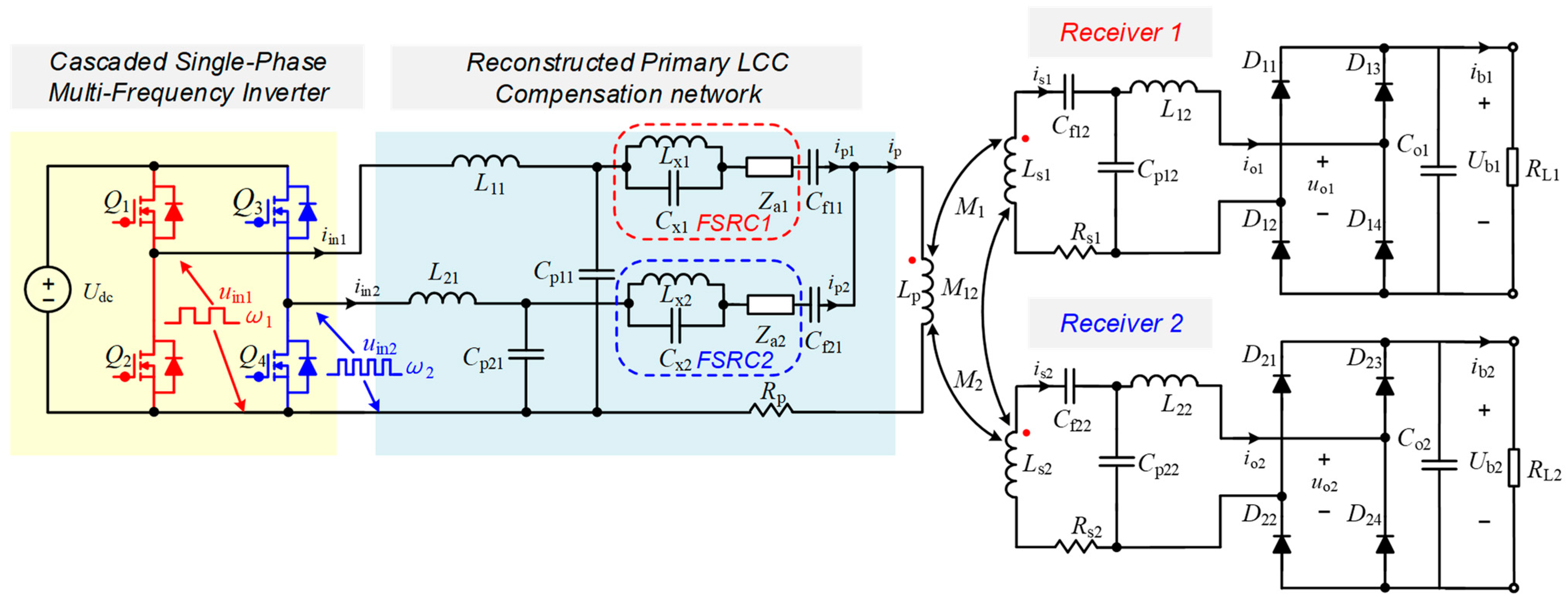
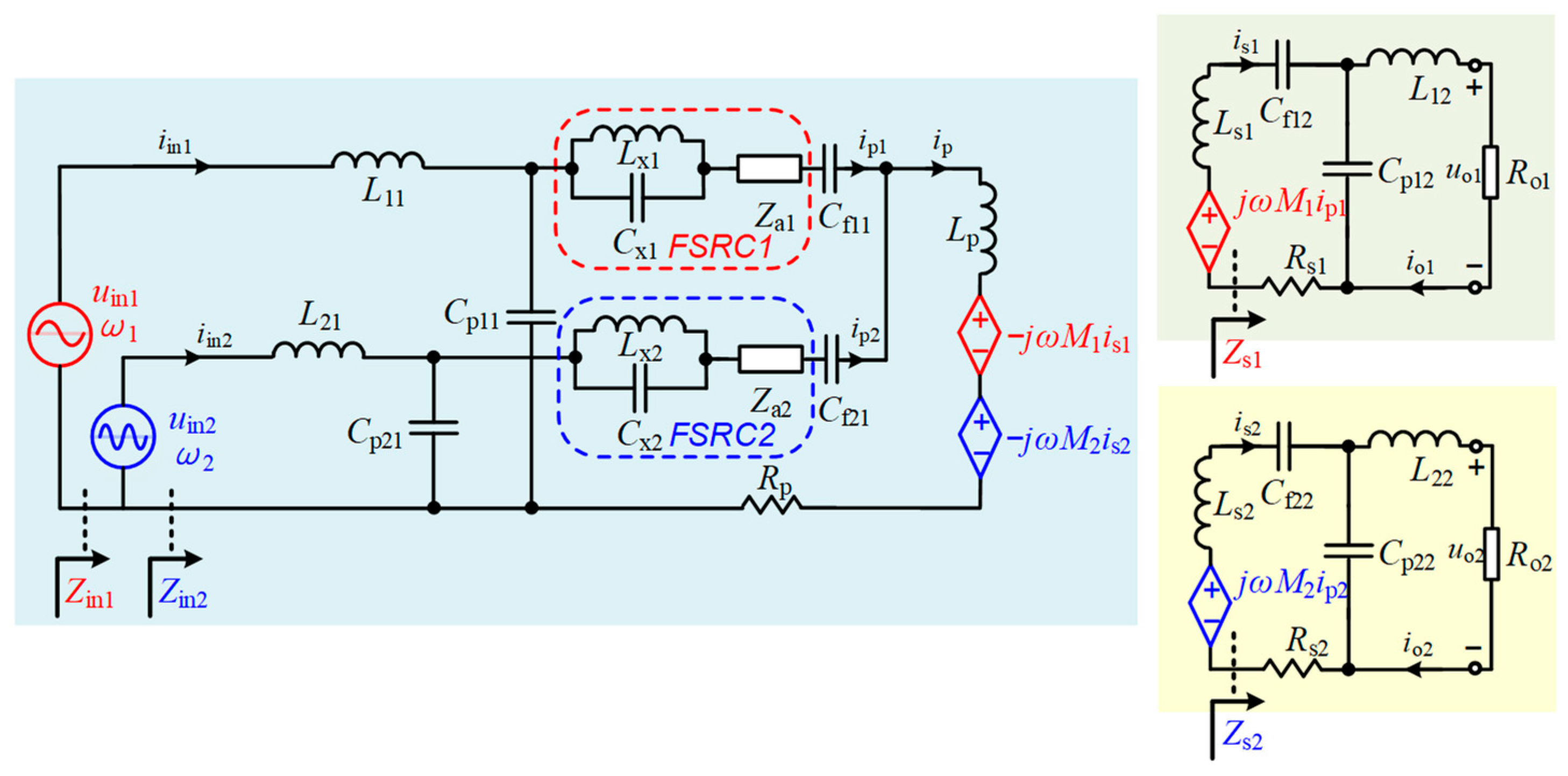
2. Theoretical Analysis of the Proposed Dual-Frequency Compatible WPT System

The schematic diagram of the proposed integrated DS-LCC compensation based dual-frequency compatible WPT system is shown in Figure 1. The entire system constitutes a CSMI, a reconstructed primary LCC compensation network, and two receivers. Among these, the cascaded multi-frequency inverter is composed of two half-bridge inverters, and it is utilized to convert the common dc-link voltage Udc to the ac voltages uini (i = 1, 2) at two specified resonant frequency ω1 and ω2. It should be noted that the subscript “i” represents the number of channels corresponding to the two resonant frequencies, which will not be repeated in subsequent sections. In practical, two full-bridge inverter also can be used to construct the system. Compared with full-bridge inverters, the use of half-bridge inverters can reduce the utilization rate of dc bus voltage, but it allows two transmission channels to share a dc power supply and a common ground wire and can reduce the number of power switch, which reduces the volume and cost of the system and improve the integration, this is the main reason why we use cascaded half-bridge structure. Generally, uini is a half-square wave with a fixed duty cycle of 0.5, and the fundamental harmonic analysis (FHA) method is used for qualitative analysis. In this case, only the fundamental harmonic of uini is considered, and its root mean square (RMS) value is denoted as Uini, and can be derived as:
U i n i = U i n i · = 2 π U dc ,   i = 1 , 2
In the primary side, two LCC compensation networks are cascaded and reconstructed based on the FSRC network, so as to provide independent dual-frequency power transmission channels. Each reconstructed primary LCC compensation network comprises a resonant inductor Li1, two resonant capacitors Cpi1 and Cfi1, and a FSRC network. In order to suppress the crosstalk between the two power transmission channels and ensure the independence of the dual-frequency signals, the FSRC network is utilized to provide a path for the power signal transmission at the target resonant frequency and block the power signal transmission at another resonant frequency. The specific working principle and parameter design criteria of the FSRC network will be discussed in subsequent sections. By reconstructing the primary LCC compensation network, the loop currents of the two power transmission channels ip1 and ip2 can be superimposed into a single transmitting coil to reduce the cost and volume of the system.
In the secondary side, the two receivers are composed of two receiving coils, two normal LCC compensation networks, two single-phase bridge rectifiers (SBR), and two dc loads. Among these, the SBR is used to convert the ac voltage uoi to the charging voltage Ubi, and a dc capacitor Coi is used to stabilize Ubi. Under this scenario, the inputs and outputs of the SBR have the following relationships:
U b i = π 2 4 U o i I b i = 2 2 π I o i ,   i = 1 , 2
where Uoi and Ioi are the RMS values of the AC inputs of each SBR. Based on (2), an ac equivalent resistance Roi can be deduced as:
R o i = 8 π 2 R L i ,   i = 1 , 2
For the loosely coupled transformer (LCT), a transmitting coil and two receiving coils form a three-coil structure. Lp is the self-inductance of the single transmitting coil, Ls1 and Ls2 are the self-inductance of the two receiving coils. M1 and M2 are the mutual inductance between the single transmitting coil and two receiving coils, M12 is the mutual inductance between the two receivers. The coupling coefficient of the LCT is defined as
k 1 = M 1 L p L s 1 ,   k 2 = M 2 L p L s 2 ,   k 12 = M 12 L s 1 L s 2
According to some previous literatures [17,27], it can be known that when two receiving coils are overlapped slightly or separated from each other by a distance, the cross-coupling effect can be ignorable, namely, k12 << 1. Therefore, only the cross-coupling between the single transmitting coil and two receiving coils is considered in this paper. Under this condition, and according to Equations (1) and (2), the CSMI and SBR in Figure 1 can be replaced by two sinusoidal voltage sources and an AC equivalent load, respectively. Meanwhile, the LCT is considered equivalent to a mutual-inductance model based on the transformer theory. As a result, the proposed DS-LCC dual-frequency compatible WPT system in Figure 1 can be simplified as a mutual-inductance model-based equivalent circuit to simplify the analyses and calculations, as shown in Figure 2.
In Figure 2, it should be noted that although both receivers and the common transmitter are coupled, because the receiving circuit has a high impedance at a non-resonant frequency and the FSRC network can suppress the crosstalk between the dual-frequency power transmission channels, the equivalent circuit operating at two different frequencies can be analyzed and calculated independently. In the primary side, according to the analysis of LCC resonant network in previous literatures, when the inductor Li1 and capacitor Cpi1 are resonant, i.e., ωi 2 = 1/(Li1Cpi1), the load-independent primary side loop current in each power transmission channels can be deduced as:
I pi · = U ini · j ω i L i 1 = U ini ω i L i 1 90 , i = 1 , 2
According to the Kirchhoff’s current law (KCL), the dual-frequency superposition current passing through the primary side coil is
I p · = I p 1 · + I p 2 ·
On the basis of satisfying Equation (5), if the resonant condition ωi2 = 1/(LseiCpi2) is also satisfied in each secondary side, where Lsei is the equivalent inductance that includes the series connection of Lsi and Cfi2, and Lsei = Lsi − 1/(ωi2Cfi2), the load-independent ac output current in each receiver can be deduced as:
I o i · = M i U ini · j ω i L i 1 L sei 1 = M i U ini j ω i L i 1 L sei 1 90 ° , i = 1 , 2

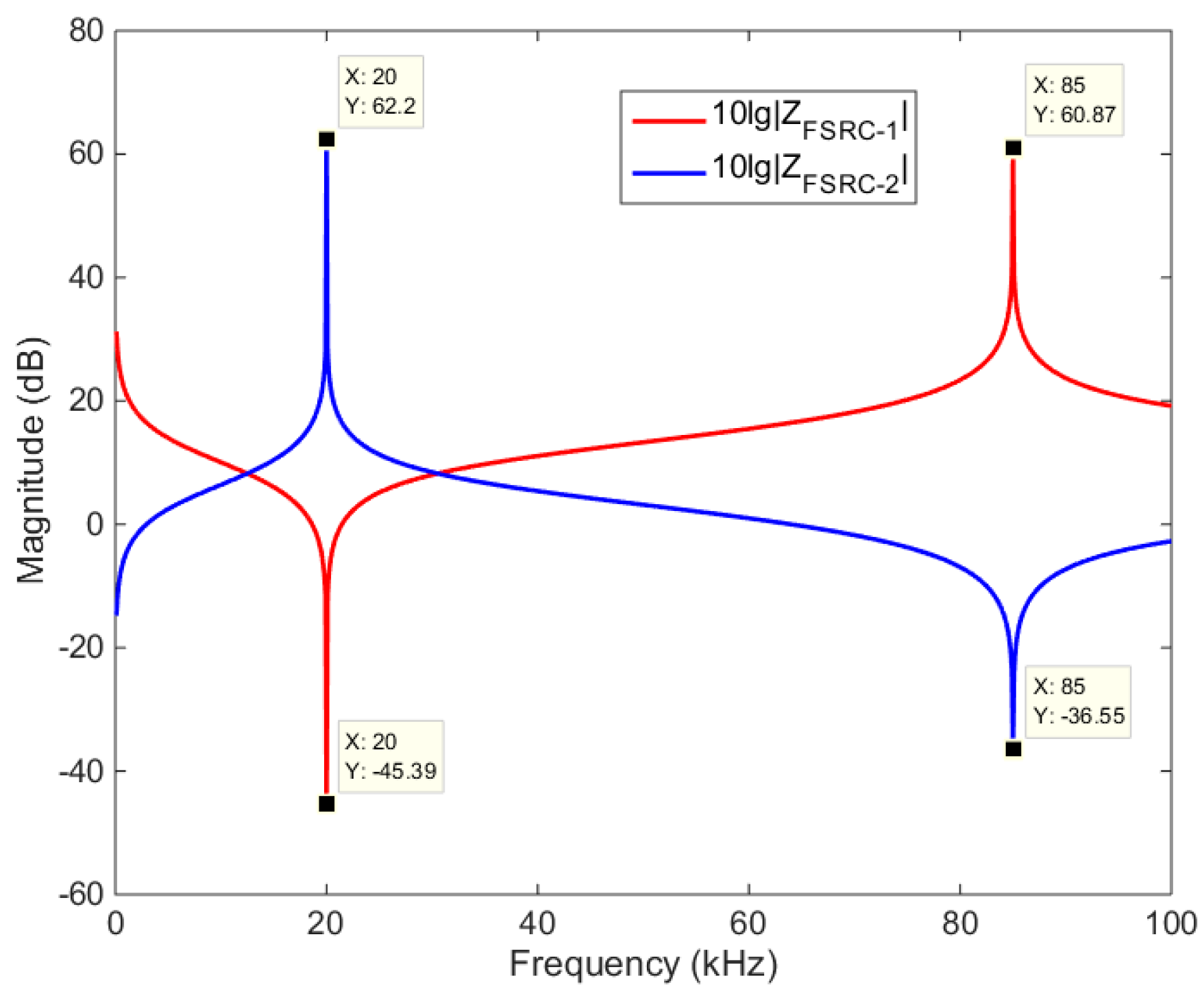
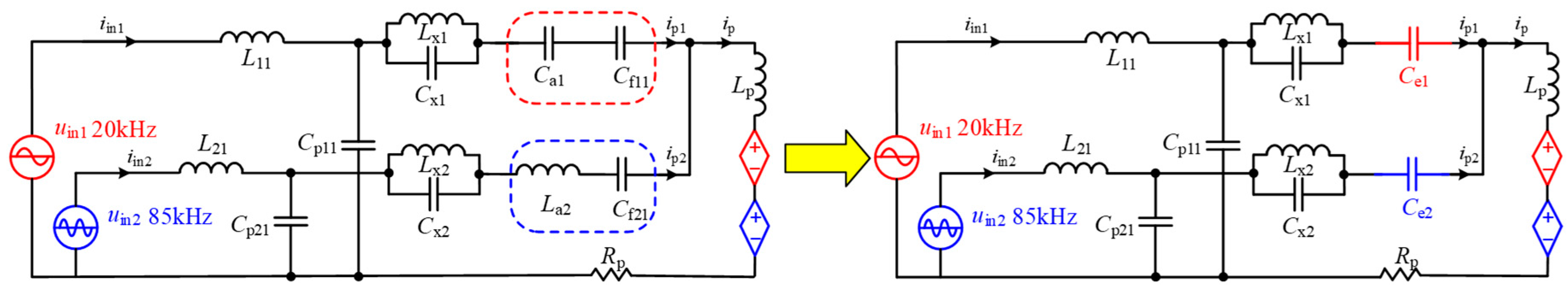
3. Working Principle and Parameter Design Criteria of the FSRC Network

According to the above analysis, in order to implement the load-independent CCO of the dual-frequency power transmission channels in the proposed system, it is not only necessary to satisfy the resonant conditions associated with CCO characteristics, but more importantly, to suppress the crosstalk between the dual-frequency channels by utilizing the FSRC networks. Thus, in this section, the construction method of the FSRC network for dual-frequency power transfer is considered in detail.
As shown in Figure 2, the equivalent impedance of the FSRC network can be derived as:
Z FSRC _ i = 1 1 / j ω L x i + j ω C x i + Z ai   = j ω L x i 1 ω 2 L x i C x i + Z ai
For each power transmission channel, the basic working principle of the FSRC network is to provide a power transmission path at the target resonant frequency and block the power signal transmission at another resonant frequency, i.e.,
lim ω ω on Z FSRC _ i = 0   lim ω ω off Z FSRC _ i =
where ωon is the natural resonant frequency of one power transmission channel, and ωoff is the natural resonant frequency of another power transmission channel. By combining Equations (8) and (9), the following relational expressions are obtained:
1 = ω off 2 L x i C x i   Z ai = j ω on L x i 1 ( ω on / ω off ) 2
From Equation (10), it can be seen that if ωon >ωoff, Zai is a positive complex number, i.e., Zai consists of an inductor Lai (Zai = jωonLai), and Lai can be calculated as
L ai = ω off 2 L x i ω on 2 ω off 2
If ωon < ωoff, Zai is a negative complex number, i.e., Zai consists of a capacitor Cai (Zai = 1/jωonCai), and Cai can be calculated as
C ai = ω off 2 ω on 2 L x i ω on 2 ω off 2
For a multi-frequency WPT system, when the resonant frequencies of different power transmission channels are relatively close, there will be obvious crosstalk issue, resulting in the analysis and design of the system are not accurate. In order to avoid this issue, under the premise of meeting application requirements and constraints, the difference between each operating frequency should be improved as much as possible in the design. In this paper, the two resonant frequencies are specified as ω1 = 125,664 rad/s (f1 = 20 kHz), and ω2 = 534,071 rad/s (f2 = 85 kHz). According to the above analysis, the structures of the two FSRC networks in Figure 2 can be determined, as shown in Figure 3.
The function of FSRC 1 is to provide a power transmission path at ω1 and block the power signal transmission at ω2, and the function of FSRC 2 is just the opposite. In order to realize the above functions, the parameters of the two FSRC networks need to be designed. First, in the two FSRC networks, the parallel resonant inductor Lxi has no parameter constraint and has high parameter design freedom. Considering that a too large inductance value of Lxi will increase the cost and volume, while a too small value of Lxi will introduce large parameter errors. On balance, the inductance of Lx1 and Lx2 in Figure 3 are designed to be 50 μH. Next, according to the two resonant frequencies ω1 and ω2, and by using Equations (10)–(12), the values of the remaining resonant parameters in the two FSRC networks can be obtained separately. The designed resonant parameters are listed in Table 1.
Using the parameters listed in Table 1, the impedance magnitude of ZFSRC_i versus frequency is calculated by using MATLAB 2021a tool, as shown in Figure 4. The red and blue curves represent the variation of the impedance of ZFSRC_1 and ZFSRC_2 with frequency, respectively. It should be noted that in order to make the curve easier to navigate, the logarithmic representation is used to normalize the magnitude of ZFSRC_i. When f = 20 kHz, the impedance magnitude of ZFSRC_1 is close to zero, while the impedance magnitude of ZFSRC_2 is close to infinity, while when f = 85 kHz, the impedance magnitude of ZFSRC_2 is close to zero, while the impedance magnitude of ZFSRC_1 is close to infinity. Figure 4 show that the FSRC 1 network has a conduction effect on the 20 kHz power signal, and a blocking effect on the 85 kHz power signal, while the FSRC 2 network has a conduction effect on the 85 kHz power signal, and a blocking effect on the 20 kHz power signal. The above analysis results show that the structure and parameter design of FSRC networks meet the requirements of dual-frequency power transmission.

4. Parameter Design Method of the Proposed Dual-Frequency WPT System

For the DS-LCC compensated WPT system, CCO and zero phase angle (ZPA) are two major considerations for parameter tuning. Since the implementation of CCO for the DS-LCC compensation based dual-frequency WPT system has been given in Section 2, the implementation of ZPA should be discussed here.
In Figure 2, the total equivalent impedances of the secondary and primary sides in two power transmission channels are defined as Zsi and Zini, respectively, and they can be calculated as
Z s i =       j ω L si + R si + 1 / j ω C fi 2 + 1 / j ω C pi 2   ( j ω L i 2   +   R oi ) 1 / j ω C pi 2   +   j ω L i 2   +   R oi Z ini =   j ω L i 1 + 1 / j ω C pi 1   ( j ω L p   +   1 / j ω C fi 1 + R p + Z ri + Z FSRC _ i ) 1 / j ω C pi 1   + j ω L p   +   1 / j ω C fi 1 + R p + Z ri + Z FSRC _ i
where Zri is the reflected impedance. Zri is converted from the secondary side to the primary side, and is deduced as: Zri = ω2Mi2/Zsi. The phase angles of the Zsi and Zini are defined as:
θ s i = 18 0 ° π tan 1 Im Z s i Re Z s i θ ini = 18 0 ° π tan 1 Im Z ini Re Z ini
In the DS-LCC compensation based dual-frequency WPT system, θsi and θini should generally be tuned to zero to minimize VA rating of the system. For an LCC compensation network, as shown in Figure 2, the decisive condition for ZPA is that the equivalent inductance of both arms is equal, and both resonate with the parallel compensation capacitance. In each secondary side, when the resonant condition ωi2 = 1/(LseiCpi2) is satisfied, the condition for θsi to be zero is Lsei = Li2. Based on this, by combining Equations (2) and (7), the constant charging currents of both receivers can be deduced as:
I b i = 2 2 M i U ini π ω i L i 1 L i 2
In this paper, based on existing experimental conditions and application requirements, a set of system-level parameters are specified, as listed in Table 2.
During the parameter design process of a DS-LCC compensated WPT system, firstly, it is necessary to calculate the double-side compensation inductances according to the specified constant charging current value. In this paper, in order to simplify the design process, we consider the design of the double-side compensation inductances as symmetric. Thus, by using the parameters listed in Table 2 and Equation (15), the double-side compensation inductances in dual-frequency channels can be calculated as: L11 = L12 = 57.79 µH, and L21 = L22 = 28.03 µH.
After determining the double-side compensation inductances, all remaining capacitances in the system can be calculated based on the aforementioned CCO and ZPA conditions. In the primary side, because both the impedance magnitude of ZFSRC_1 and ZFSRC_2 are close to zero, the condition for θini to be zero is Li1 = Lp − 1/(ωi2Cfi1). Thus, the normalized capacitances of Cf11 and Cf21 can be calculated as 206.6 nF and 10.43 nF, respectively. However, in practical WPT applications, it is necessary to fine-tune the normalized resonant parameters to achieve the ZVS of the inverter. For a normal DS-LCC compensated WPT system, introducing 5~10% reduction in the normalized Cfi1 is a common way to implement ZVS without sacrificing the CCO characteristics of the system. As a result, the practical capacitances of Cf11 and Cf21 in this paper are ultimately designed to be 190 nF and 9.5 nF, respectively. The designed resonant parameters of the dual-frequency WPT system are listed in Table 3.
In addition, Zai and Cfi1 in Figure 2 can be equivalent to a total impedance, so that the redundancy of the compensation topology is reduced without affecting the frequency-selection characteristic of the FSRC networks. As shown in Figure 5, according to the parameters listed in Table 1 and Table 3, the series impedances in the red and blue dashed boxes can be equivalent to the capacitors Ce1 and Ce2, which can be calculated as:
C e 1 = C a 1 C f 1 1 C a 1 + C f 1 1   C e 2 = C f 2 1 1 ω 2 2 L a 2 C f 2 1
By substituting the relevant parameters in Table 1 and Table 3 into Equation (16), the capacitances of Ce1 and Ce2 are calculated as: 164 nF and 9.6 nF, respectively.

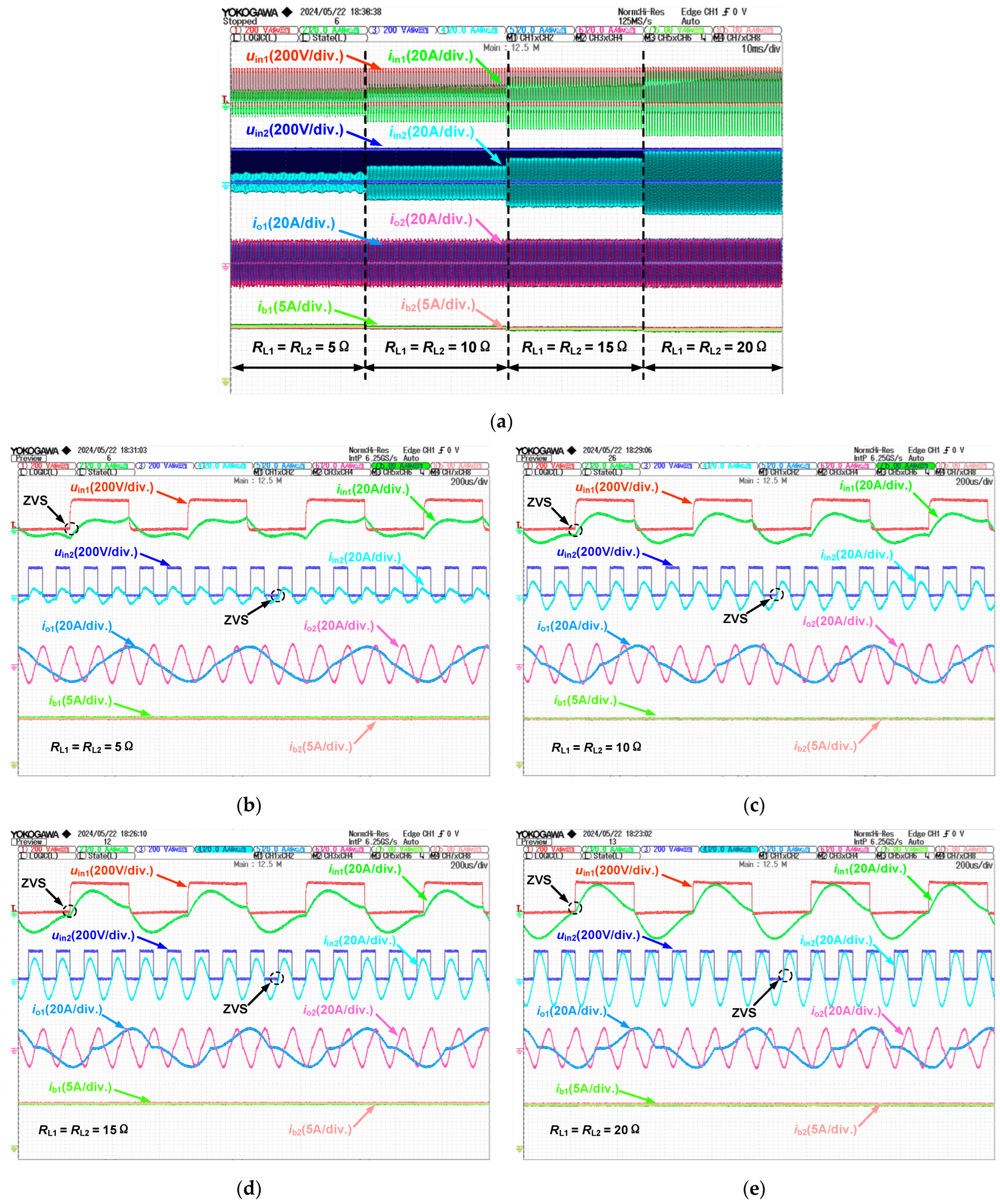
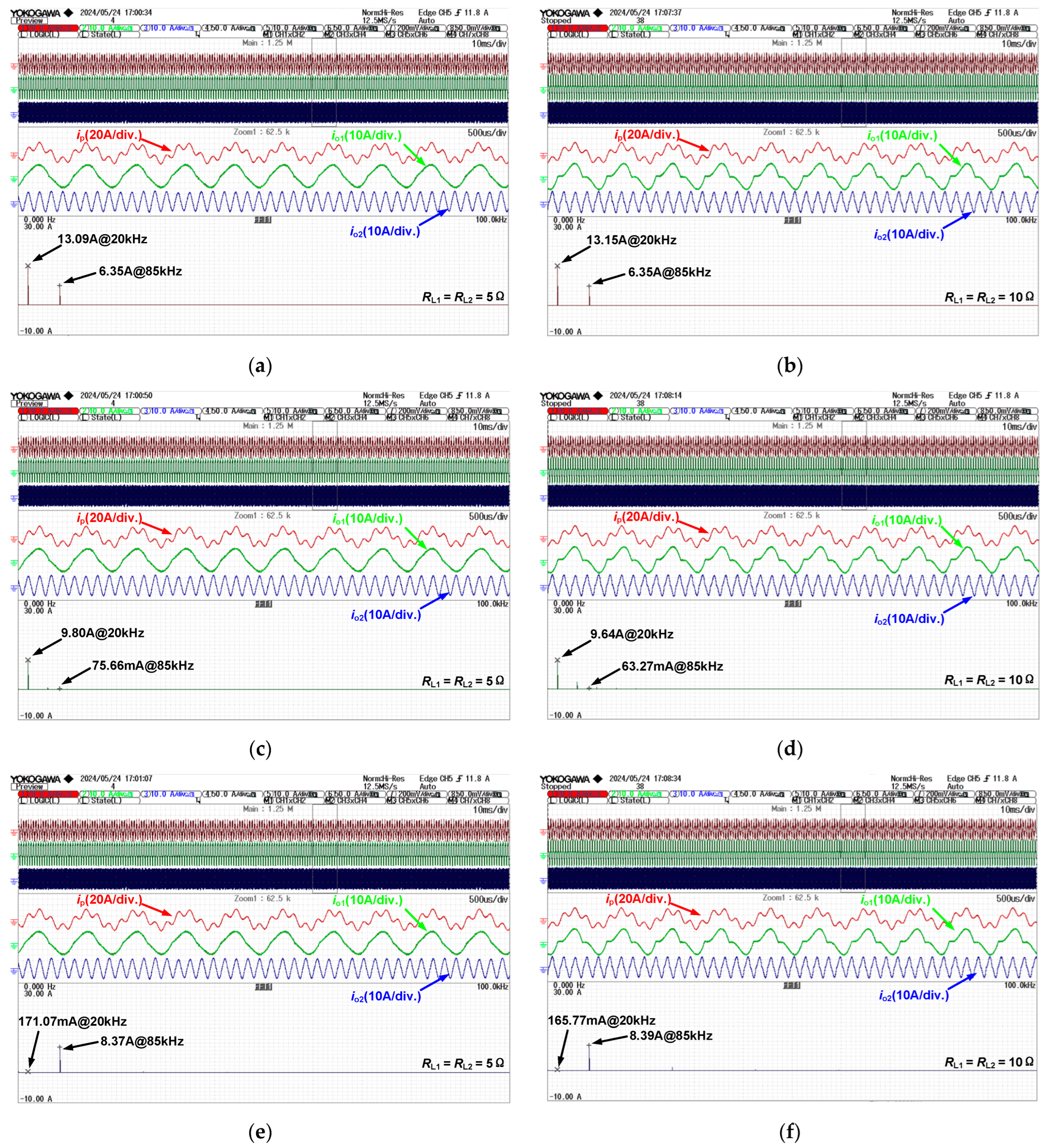
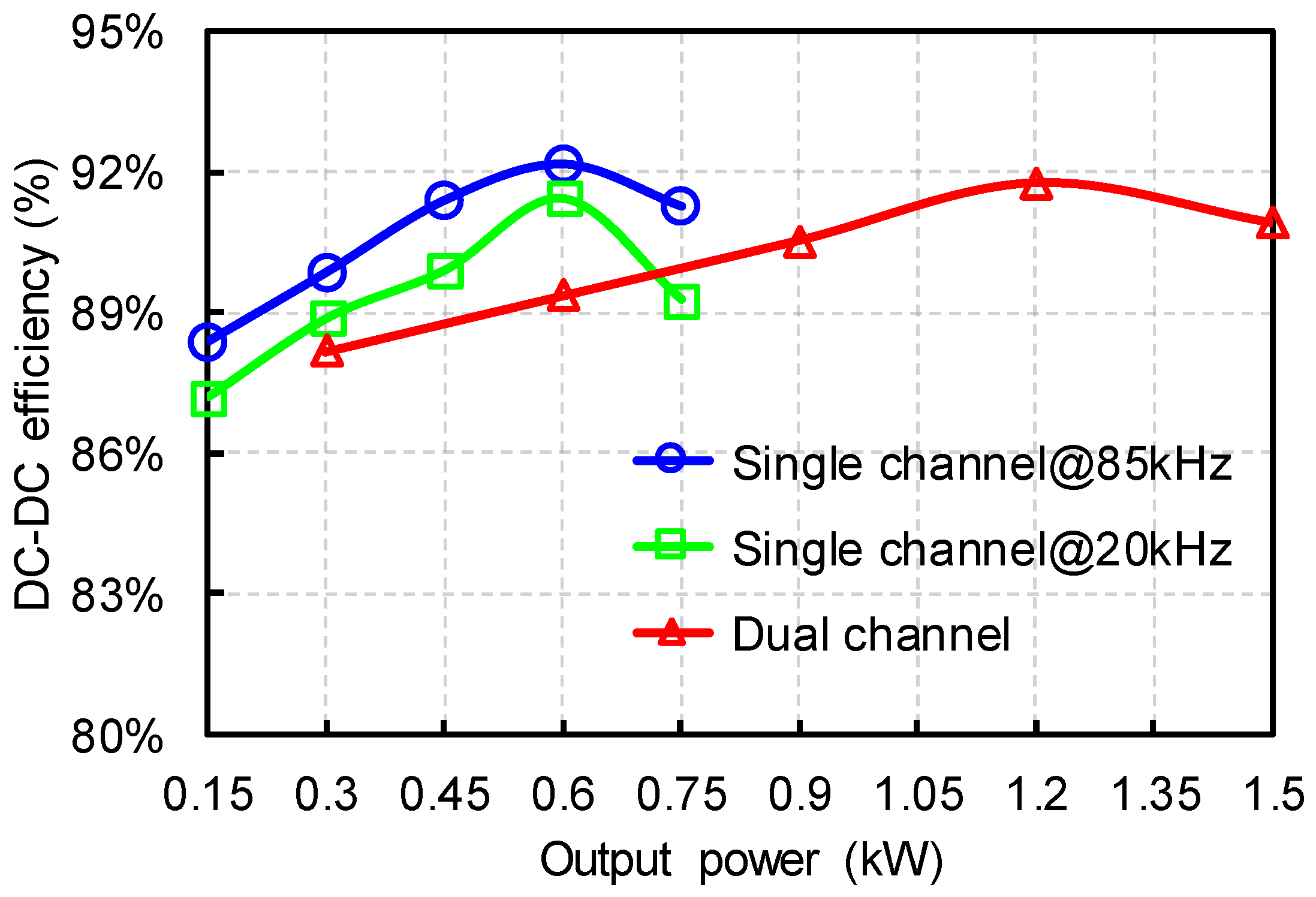
5. Experimental Verification

In order to verify the practicability and effectiveness of the presented dual-frequency compatible WPT system, a 1.5-kW experimental prototype of the DS-LCC compensation based dual-frequency WPT system is configured, as shown in Figure 6. For this study, our major considerations in the design of magnetic couplers are twofold. First, the relative distance between the two receiving coils should be as far away as possible to eliminate the coupling between the two receiving coils. Second, the position of the two receiving coils relative to the common transmitting coil should be as symmetrical as possible to ensure that the two power transmission channels have the same magnetic coupling parameters. Under these two design guidelines, we designed a set of three-coil magnetic coupler, Figure 6b and Table 4 show the practical structure and parameters of the magnetic coupler designed. It can be seen that the practical parameters of the designed magnetic coupler meet the pre-designed requirements. The practical resonant parameters are measured with an LCR meter, and the maximum deviation between the designed parameters and practical parameters is found to be less than 2%.
Based on the aforementioned experimental constructions, the experimental test of the constructed system is carried out under varying load conditions. The transient waveforms with load fluctuations are shown in Figure 7. It should be noted that in the practical charging process, the equivalent internal resistance of the battery varies continuously within a certain range, and in this study, we adopted electronic load for experimental verification. Due to the limitations of time and equipment, it is difficult to simulate the continuous change of load. Therefore, 4 load points (5 Ω, 10 Ω, 15 Ω, and 20 Ω) are uniformly selected as test samples in the whole power range. It can be seen that although the RL1 and RL2 both vary from 5 Ω to 20 Ω, the charging currents Ib1 and Ib2 are both approximately equal to 6A and remain almost constant. In addition, the CSMI can achieve ZVS operation under different load conditions. The above experimental analysis indicates that the proposed dual-frequency WPT system can implement the dual-frequency power transfer with load-independent CCO and ZPA operation.
In order to verify the dual-frequency superposition and frequency selection characteristics of the proposed system, the FFT analyses of transmission currents ip, io1, and io2 are carried out under 5 Ω and 10 Ω load conditions, respectively. As shown in Figure 8a,b, when RL1 = RL2 = 5 Ω, the magnitudes of ip1 and ip2 components are 13.09 A and 6.35 A, while when RL1 = RL2 = 10 Ω, the magnitudes of ip1 and ip2 components are 13.15 A and 6.35 A. Figure 8a,b indicate that the current of the transmitting coil ip consists of only 20 kHz and 85 kHz frequency components, and the magnitude of the two frequency components is almost constant under different load conditions. Figure 8a,b not only confirms the derivation and analysis of Equations (5) and (6), but also proves that the designed FSRC networks can superimpose the dual-frequency current components ip1 and ip2 to the transmitting coil, and the current of the transmitting coil ip has load-independent constant current characteristics. As shown in Figure 8c,d, under varying load conditions, the ac output currents io1 and io2 only contain their corresponding resonant frequency components, and there is almost no interference from another channel. In addition, both io1 and io2 present load-independent CCO characteristics, which confirms the derivation and analysis of Equation (7). The above experimental results prove that the proposed system can implement the load-independent dual-frequency power transfer.
To investigate and compare the system efficiency for different cases, the DC-DC efficiencies of the dual-frequency system are measured. First, the efficiency of the system under the independent operation of a single frequency channel is measured. As shown in Figure 9, in the power range of 150–750 W, the efficiency of both 20 kHz and 85 kHz frequency channels increases first and then decreases. Under the same power conditions, the efficiency of the 85 kHz channel is slightly higher than that of the 20 kHz channel, and we believe that the reason is that the transmission current of the 85 kHz channel is lower than that of the 20 kHz channel. In addition, the overall efficiency of the system when dual-frequency channel operate simultaneously is also measured. The variation trend of the overall efficiency of the dual-frequency WPT system is similar to that of the single-frequency channel operation, and the peak efficiency reaches 91.75% at a 1.2-kW output power.

6. Comparison and Discussion

Recently, a variety of dual-frequency WPT system have been presented to implement the independent dual-frequency power transfer. To clarify the unique contributions of the proposed dual-frequency WPT system in this article, a comprehensive performance comparison with the existing methods is presented in Table 5.
Refs. [16,17] indicate that the methods based on integration of multiple inverters via transformers can implement the ZVS operation of the multiple inverters, but cannot achieve load-independent constant output property, and the use of a large number of inverters and transformers greatly increases the design complexity and lower the system efficiency. In [18,19,20,21,22], although the methods based on SPWM and NPC-ML can reduce the design complexity, the system efficiency is still relative low because the ZVS operation cannot be satisfied. In addition, due to the limitation of system efficiency, the existing methods are difficult to apply in large power applications.
The main contributions and improvements of the proposed method over existing methods are summarized as follows:
(1)
This article reconstructed the conventional DS-LCC compensated WPT system by using CSMI and FSRC, the load-independent CCO property and ZVS operation at two specified frequencies can be implemented simultaneously.
(2)
The proposed method has low design complexity and can significantly improve the system efficiency, and can be applied to multi-frequency and multi-load wireless charging with higher power level.

7. Conclusions

In order to address the issue of hard-switching operation and power crosstalk of different frequency channels in conventional dual-frequency dual-load WPT system. This article proposes an integrated DS-LCC compensation based dual-frequency compatible WPT system to implement dual-frequency power transfer. On the basis of conventional DS-LCC compensated WPT system, the load-independent CCO and ZVS under dual-frequency power transmission condition are achieved by constructing CSMI and FSRC. The working principle of the proposed system is analyzed in detail, and the general parameter design procedure are introduced. A 1.5-kW experimental prototype is constructed to verify the rationality and feasibility of the proposed system.

Author Contributions

Conceptualization, Y.C., Y.L. and J.W.; methodology, Y.C. and Z.Y.; validation, Y.L. and Z.Y.; formal analysis, P.G.; investigation, Y.C. and Z.Y.; writing—original draft preparation, Y.C.; writing—review and editing, Y.L. and J.W. All authors have read and agreed to the published version of the manuscript.

Funding

This work was supported by the International Scientific and Technological Cooperation Projects in Henan Province under Grant 232102520003 and 242102521038, and in part by the Scientific and Technological Project in Henan Province under Grant 242102320180 and 242102320352.

Data Availability Statement

Data is contained within the article.

Conflicts of Interest

The authors declare no conflicts of interest.

References

  1. Zhang, Z.; Li, Z.; Zhang, X.; Yang, B.; He, Z.; Mai, R.; Chen, Y. A dynamic wireless power transfer system using DC controlled variable inductor for segment transmitter automatic switching. IEEE Trans. Power Electron. 2024, 1–5. [Google Scholar] [CrossRef]
  2. Chen, Y.; Zhang, Z.; Yang, B.; Zhang, B.; Fu, L.; He, Z.; Mai, R. A clamp circuit-based inductive power transfer system with reconfigurable rectifier tolerating extensive coupling variations. IEEE Trans. Power Electron. 2023, 39, 1942–1946. [Google Scholar] [CrossRef]
  3. Li, Z.; Liu, H.; Huo, Y.; He, J.; Tian, Y.; Liu, J. High-misalignment tolerance wireless charging system for constant power output using dual transmission channels with magnetic flux controlled inductors. IEEE Trans. Power Electron. 2022, 37, 13930–13945. [Google Scholar] [CrossRef]
  4. Chen, Y.; Wu, J.; Zhang, H.; Guo, L.; Lu, F.; Jin, N.; Kim, D.H. A parameter tuning method for a double sided LCC compensated IPT system with constant voltage output and efficiency optimization. IEEE Trans. Power Electron. 2023, 38, 4124–4139. [Google Scholar] [CrossRef]
  5. Chen, Y.; Zhang, H.; Jin, N.; Guo, L.; Wu, J.; Park, S.-J.; Kim, D.-H. A unipolar-duty-cycle hybrid control strategy of series–series compensated IPT system for constant-current output and efficiency optimization. IEEE Trans. Power Electron. 2022, 37, 13884–13901. [Google Scholar] [CrossRef]
  6. Lu, C.; Huang, X.; Rong, C.; Tao, X.; Zeng, Y.; Liu, M. A dual-band negative permeability and near-zero permeability metamaterials for wireless power transfer syste. IEEE Trans. Ind. Electron. 2021, 68, 7072–7082. [Google Scholar] [CrossRef]
  7. Liao, Z.-J.; Zhu, Q.-W.; Yu, Y.; Xia, C.-Y.; Rong, C.-C. Analysis and design of self-oscillating magnetic coupling wireless power transfer systems. IEEE J. Emerg. Sel. Top. Power Electron. 2024, 12, 1140–1149. [Google Scholar] [CrossRef]
  8. Zhou, W.; Chen, Z.; Zhang, Q.; Li, Z.; Huang, L.; Mai, R.; He, Z. Design and analysis of CPT system with wide-range ZVS and constant current charging operation using 6.78 MHz Class-E power amplifier. IEEE J. Emerg. Sel. Top. Power Electron. 2024, 12, 3211–3225. [Google Scholar] [CrossRef]
  9. Cai, C.; Wang, J.; Zhao, Y.; Luo, Y.; Yuan, Z.; Xue, M.; Rao, Y.; Yang, L.; Hong, Y.; Wang, C. Hybrid interference field mitigation of dual-rectangular transmitter pad for universal wireless charging area expansion. IEEE Trans. Transport. Electrific. 2024, 10, 3816–3827. [Google Scholar] [CrossRef]
  10. Li, H.; Liu, M.; Kong, L.; Wang, Y. An independent dual-coil driving topology for wireless power transfer. IEEE Trans. Power Electron. 2023, 38, 1378–1383. [Google Scholar] [CrossRef]
  11. Li, Y.; Mai, R.; Lu, L.; Lin, T.; Liu, Y.; He, Z. Analysis and transmitter currents decomposition based control for multiple overlapped transmitters based WPT systems considering cross couplings. IEEE Trans. Power Electron. 2018, 33, 1829–1842. [Google Scholar] [CrossRef]
  12. Liu, X.; Gao, F.; Wang, T.; Khan, M.M.; Zhang, Y.; Xia, Y.; Wheeler, P. A multi-inverter multi-rectifier wireless power transfer system for charging stations with power loss optimized control. IEEE Trans. Power Electron. 2023, 38, 9261–9277. [Google Scholar] [CrossRef]
  13. Luo, C.; Qiu, D.; Zhang, B.; Xiao, W.; Chen, Y. Wireless power transfer system for multiple loads. Trans. China Electrotech. Soc. 2020, 35, 2499–2516. [Google Scholar]
  14. Liu, Z.; Su, M.; Zhu, Q.; Chao, Y.; Zang, S.; Hu, A.P. A dual-frequency 3-D WPT system with directional power transfer capability at two separately regulated outputs. IEEE J. Emerg. Sel. Top. Power Electron. 2023, 11, 2514–2524. [Google Scholar] [CrossRef]
  15. Zhang, X.; Liu, F.; Mei, T. Multifrequency phase-shifted control for multiphase multiload MCR WPT system to achieve targeted power distribution and high misalignment tolerance. IEEE Trans. Power Electron. 2021, 36, 991–1003. [Google Scholar] [CrossRef]
  16. Huang, Y.; Liu, C.; Xiao, Y.; Liu, S. Separate power allocation and control method based on multiple power channels for wireless power transfer. IEEE Trans. Power Electron. 2020, 35, 9046–9056. [Google Scholar] [CrossRef]
  17. Liu, F.; Yang, Y.; Ding, Z.; Chen, X.; Kennel, R.M. A multifrequency superposition methodology to achieve high efficiency and targeted power distribution for a multiload MCR WPT system. IEEE Trans. Power Electron. 2018, 33, 9005–9016. [Google Scholar] [CrossRef]
  18. Xia, C.; Wei, N.; Zhang, H.; Zhao, S.; Li, Z.; Liao, Z. Multifrequency and multiload MCR-WPT system using hybrid modulation waves SPWM control method. IEEE Trans. Power Electron. 2021, 36, 12400–12412. [Google Scholar] [CrossRef]
  19. Qi, C.; Huang, S.; Chen, X.; Wang, P. Multifrequency modulation to achieve an individual and continuous power distribution for simultaneous MR-WPT system with an inverter. IEEE Trans. Power Electron. 2021, 36, 12440–12455. [Google Scholar] [CrossRef]
  20. Gao, X.; Du, B.; Zhang, Y.; Cui, S. A dual-frequency compatible wireless power transfer system with a single transmitter and multiple receivers. IEEE Access 2022, 10, 102564–102574. [Google Scholar] [CrossRef]
  21. Liu, Y.; Liu, C.; Huang, R.; Song, Z. Primary multi-frequency constant-current compensation for one-to-multiple wireless power transfer. IEEE Trans. Circuits Syst. II Exp. Briefs 2023, 70, 2201–2205. [Google Scholar] [CrossRef]
  22. Liu, Y.; Liu, C.; Gao, X.; Liu, S. Design and control of a decoupled multichannel wireless power transfer system based on multilevel inverters. IEEE Trans. Power Electron. 2022, 37, 10045–10060. [Google Scholar] [CrossRef]
  23. Pang, H.; Chau, K.T.; Han, W.; Liu, W.; Zhang, Z. Decoupled-double D coils based dual-resonating-frequency compensation topology for wireless power transfer. IEEE Trans. Magn. 2022, 58, 1–7. [Google Scholar] [CrossRef]
  24. Thenathayalan, D.; Park, J.-H. Individually regulated multiple-output WPT system with a single PWM and single transformer. IEEE J. Emerg. Sel. Top. Power Electron. 2020, 8, 3542–3557. [Google Scholar] [CrossRef]
  25. Zhang, Z.; Zhang, B. Angular-misalignment insensitive omnidirectional wireless power transfer. IEEE Trans. Ind. Electron. 2020, 64, 2755–2764. [Google Scholar] [CrossRef]
  26. Kim, Y.-J.; Ha, D.; Chappell, W.J.; Irazoqui, P.P. Selective wireless power transfer for smart power distribution in a miniature-sized multiple-receiver system. IEEE Trans. Ind. Electron. 2016, 63, 1853–1862. [Google Scholar] [CrossRef]
  27. Zhang, Z.; Pang, H. Continuously adjustable capacitor for multiple-pickup wireless power transfer under single-power-induced energy field. IEEE Trans. Ind. Electron. 2020, 67, 6418–6427. [Google Scholar] [CrossRef]
  28. Hou, X.; Wang, Z.; Su, Y.; Liu, Z.; Deng, Z. A dual-frequency dual-load multi-relay magnetic coupling wireless power transfer system using shared power channel. IEEE Trans. Power Electron. 2022, 37, 15717–15727. [Google Scholar] [CrossRef]
  29. Pang, H.; Chau, K.T.; Liu, W.; Tian, X. Multi-resonating compensation for multi-channel multi-pickup wireless power transfer. IEEE Trans. Magn. 2022, 58, 1–6. [Google Scholar] [CrossRef]
  30. Cheng, C.; Zhou, Z.; Li, W.; Zhu, C.; Deng, Z.; Mi, C.C. A multi-load wireless power transfer system with series-parallel-series compensation. IEEE Trans. Power Electron. 2019, 34, 7126–7130. [Google Scholar] [CrossRef]
Figure 1. Schematic diagram of the proposed integrated DS-LCC compensation based dual-frequency compatible WPT system.
Electronics 13 03714 g001
Figure 2. Mutual-inductance model-based equivalent circuit of the proposed integrated DS-LCC compensation based dual-frequency compatible WPT system.
Electronics 13 03714 g002
Figure 3. Schematic diagram of the FSRC networks at two resonant frequencies (a) Structure of the FSRC 1 (ωon = ω1 = 125,664 rad/s, while ωoff = ω2 = 534,071 rad/s); (b) Structure of the FSRC 2 (ωon = ω2 = 534,071 rad/s, while ωoff = ω1 = 125,664 rad/s).
Electronics 13 03714 g003
Figure 4. Calculated impedance magnitude of ZFSRC_i versus frequency.
Electronics 13 03714 g004
Figure 5. Equivalent diagram of the primary LCC compensation network.
Electronics 13 03714 g005
Figure 6. Experimental prototype of the of the DS-LCC compensation based dual-frequency WPT system. (a) Overall structure and component identification of the system; (b) Structure and dimensions of the LCT.
Electronics 13 03714 g006aElectronics 13 03714 g006b
Figure 7. Transient waveforms with load fluctuations (a) RL1 and RL2 vary from 5 Ω to 20 Ω; (b) Enlarged view of the transient waveforms at RL1 = RL2 = 5 Ω; (c) Enlarged view of the transient waveforms at RL1 = RL2 = 10 Ω; (d) Enlarged view of the transient waveforms at RL1 = RL2 = 15 Ω; (e) Enlarged view of the transient waveforms at RL1 = RL2 = 20 Ω.
Electronics 13 03714 g007
Figure 8. FFT analyses of transmission currents ip, io1, and io2 (a) FFT analysis of ip at RL1 = RL2 = 5 Ω; (b) FFT analysis of ip at RL1 = RL2 = 10 Ω; (c) FFT analysis of io1 at RL1 = RL2 = 5 Ω; (d) FFT analysis of io1 at RL1 = RL2 = 10 Ω; (e) FFT analysis of io2 at RL1 = RL2 = 5 Ω; (f) FFT analysis of io2 at RL1 = RL2 = 10 Ω.
Electronics 13 03714 g008
Figure 9. Measured DC-DC efficiency versus output power for different cases.
Electronics 13 03714 g009
Table 1. Designed parameters of the two FSRC networks.
NoteSymbolValue
Resonance frequency of FSRC 1f120 kHz
Resonance frequency of FSRC 2f285 kHz
Parallel resonant inductance of FSRC 1Lx150 µH
Parallel resonant inductance of FSRC 2Lx250 µH
Parallel resonant capacitance of FSRC 1Cx170.12 nF
Parallel resonant capacitance of FSRC 2Cx21266.51 nF
Series resonant capacitance of FSRC 1Ca11196.40 nF
Series resonant inductance of FSRC 2La22.93 µH
Table 2. Specified system-level parameters of the dual-frequency WPT system.
NoteSymbolValue
DC-link input voltageUdc150 V
Resonance frequency of channel 1f120 kHz
Resonance frequency of channel 2f285 kHz
Charging current of channel 1 Ib16 A
Charging current of channel 2 Ib26 A
Primary coil inductanceLp364.3 µH
Secondary coil inductance of channel 1Ls1227.1 µH
Secondary coil inductance of channel 2Ls2227.1 µH
Mutual inductance of channel 1M141.42 µH
Mutual inductance of channel 2M241.42 µH
Table 3. Designed resonant parameters of the dual-frequency WPT system.
NoteSymbolValue
Dual-side resonant inductances of channel 1L11 & L1257.79 µH
Dual-side resonant inductances of channel 2L21 & L2228.03 µH
Dual-side parallel resonant capacitances of channel 1Cp11 & Cp121095.8 nF
Dual-side parallel resonant capacitances of channel 1Cp21 & Cp22125.1 nF
Primary series resonant capacitances of channel 1Cf11190.0 nF
Primary series resonant capacitances of channel 2Cf219.5 nF
Secondary series resonant capacitances of channel 1Cf12374.0 nF
Secondary series resonant capacitances of channel 2Cf2217.6 nF
Table 4. Measured dimensional and magnetic parameters of the LCT.
ParameterValue
Air gap distance
Turns per coil
100 mm
Np: 21; Ns1: 30; Ns2: 30
Primary coil dimensions790 mm × 240 mm (Outer size)
660 mm × 110 mm (Inner size)
Secondary coil dimensions230 mm (Outer size); 70 mm (Inner size)
Litz wire dimensionsAWG 9 (2.91 mm)
Secondary coil center distance
Primary coil inductance Lp
Secondary coil inductance of channel 1 Ls1
Secondary coil inductance of channel 2 Ls2
Coupling coefficient between transmitter and receiver 1 k1
Coupling coefficient between transmitter and receiver 1 k2
Coupling coefficient between receiver 1 and 2 k12
600 mm
362.9 µH
228.3 µH
228.3 µH
0.145
0.143
0.003
Table 5. Summary and comparison of the existing dual-frequency WPT system.
ReferenceMulti-Frequency Superposition MethodMaximum
Efficiency
ZVS OperationOperating
Frequency
CV/CCTopology StructureDesign
Complexity
Rating
POWER
[16]Integration of multiple inverters via transformers80%Yes176.7 kHz &
206.3 kHz
NoLCL-SHigh65 W
[17]86.7%Yes190 kHz & 210 kHzNoS-SHigh100 W
[18]Hybrid modulation waves sinusoidal pulse width modulation 70%No20 kHz &
80 kHz
CCS-SMedium40 W
[19]85%No100 kHz &
200 kHz
NoS-SMedium120 W
[20]88%No20 kHz &
85 kHz
CVLCC-SMedium100 W
[21]Neutral point clamped-multilevel inverters78.9%No100 kHz &
300 kHz
CVLCC-SMedium125 W
[22]89.3%No100 kHz &
200 kHz
CVLCC-SMedium1000 W
This articleCascaded single-phase multi-frequency inverter91.75%Yes20 kHz &
85 kHz
CCDS-LCCLow1500 W
Disclaimer/Publisher’s Note: The statements, opinions and data contained in all publications are solely those of the individual author(s) and contributor(s) and not of MDPI and/or the editor(s). MDPI and/or the editor(s) disclaim responsibility for any injury to people or property resulting from any ideas, methods, instructions or products referred to in the content.

