Article

Improving the Light Extraction Efficiency of GaN-Based Thin-Film Flip-Chip Micro-LEDs through Inclined Sidewall and Photonic Crystals

College of Physics and Electronics Engineering, Qilu Normal University, Jinan 250200, China
*
Author to whom correspondence should be addressed.
Electronics 2024, 13(18), 3750; https://doi.org/10.3390/electronics13183750
Submission received: 20 August 2024 / Revised: 13 September 2024 / Accepted: 19 September 2024 / Published: 21 September 2024

Abstract

:
Low light extraction efficiency (LEE) remains a critical bottleneck in the performance of contemporary micro-light-emitting diodes (micro-LEDs). This study presents an innovative approach to improve the LEE of Gallium nitride (GaN)-based thin-film flip-chip (TFFC) micro-LEDs by integrating an inclined sidewall with photonic crystals (PhCs). Three-dimensional finite-difference time-domain (FDTD) simulations reveal that the inclined sidewall design significantly increases the escape probability of light, thereby improving LEE. Additionally, the PhCs’ structure further improves LEE by enabling more light to propagate into the escape cones through diffraction. Optimal results are achieved when the inclined sidewall angle (θ) is 28° and the PhCs exhibit a period (a) of 220 nm, a filling factor (f) of 0.8, and a depth (d) of 3 μm, resulting in a maximum LEE of 36.47%, substantially surpassing the LEE of conventional planar TFFC micro-LEDs. These results provide valuable design guidelines for the development of high-efficiency GaN-based micro-LEDs.

1. Introduction

Gallium nitride (GaN)-based micro-light-emitting diodes (micro-LEDs) have emerged as a promising light source for a diverse array of applications, including high-brightness/contrast large flat-panel displays, visible-light communication, along with augmented and virtual reality, etc. [1]. Hang et al. [2] indicated that as the chip size of micro-LEDs decreases, several advantages are observed, such as increased peak brightness, improved contrast, reduced power consumption, and extended lifespan. However, despite these benefits, this technology still faces several challenges. One significant obstacle for commercial adoption is the low external quantum efficiency (EQE), with poor light extraction efficiency (LEE) being identified as a primary contributor to this issue [3]. The internal quantum efficiency (IQE) of GaN-based micro-LEDs has nearly reached 100% due to developments in lattice-matched epitaxial growth technology [4]. Moreover, this problem also exists in some emerging LEDs, such as perovskite LEDs [5,6]. Therefore, improving the LEE is crucial for the micro-LEDs industry to overcome existing limitations and improve performance [7].
Various strategies have been proposed to address this issue, such as nanopatterned sapphire substrates (NPSS) [8], surface texture [9], and chip-shaping technologies [10]. However, limited studies have focused on improving the LEE of micro-LEDs through optimizing chip geometry, particularly concerning different inclined sidewall angles. The inclined sidewall angle significantly impacts the light propagation path within the chip, especially in micro-LEDs with sizes in the micrometer range [3]. Kang et al. [11] and Gou et al. [12] highlighted the importance of sidewall emission in angular emission characteristics. Therefore, the precise design of the inclined sidewall angle and conducting comprehensive 3D simulations encompassing the entire micro-LED chip are essential steps to improve LEE. Photonic crystals (PhCs) have attracted much attention during the last decade as an effective tool to overcome the low LEE of LEDs [13]. Yuan et al. [14] designed SiO2 PhCs to couple with the radiative emission of perovskite nanocrystals and acquired flexible high fluorescence enhancement factors of different emission colors. Flexible PhCs have also been used to enhance the fluorescence of CsPbBr3 perovskite nanocrystals, and a stable fluorescence enhancement factor higher than fivefold was achieved under excitation of 3.97 W cm−2 [15].
Flip-chip (FC) LEDs typically exhibit superior performance compared to conventional planar and vertical LEDs due to the absence of a front electrode that could obstruct emitted light. Additionally, the back electrode in FC LEDs can be thickened to serve as the back reflector while conducting the current, which can further improve the LEE. In practice, micro-LEDs commonly utilize a thin-film flip-chip (TFFC) structure where the substrate is detached using an excimer laser. The elimination of the sapphire substrate can reduce the optical crosstalk in FC micro-LEDs [16], though it may also introduce additional internal reflections, leading to decreased LEE. Nevertheless, combining the aforementioned strategies offers a promising approach to effectively enhancing the LEE of TFFC micro-LEDs [17].
Furthermore, due to the challenges in determining LEE through experimental means, the evaluation of LEDs’ LEE has predominantly relied on numerical simulations. This approach not only saves time and resources but also allows for a comprehensive analysis. The finite-difference time-domain (FDTD) method has been extensively utilized in investigating the optical properties and LEE of LEDs featuring micro- or nanoscale structures [18].
In this study, a structure comprising inclined sidewall and PhCs was incorporated into GaN-based TFFC micro-LEDs. Three-dimensional FDTD simulations were utilized to elucidate the mechanisms through which the inclined sidewall and PhCs improved LEE. The inclined sidewall in the micro-LEDs demonstrates considerable potential for improving LEE by providing more opportunities for light to escape. Additionally, the PhCs facilitate a higher number of photons to be diffracted by the air cavity, thereby effectively improving LEE and resulting in a substantial increase in LEE. The results indicate that the overall LEE of the optimized GaN-based TFFC micro-LEDs reaches 36.47%. This represents a 238.5% enhancement of LEE compared to conventional planar TFFC micro-LEDs. The LEE enhancement compared with that of the previous work is shown in Table 1. From Table 1, we can see that the method proposed in this paper is better than the methods presented in most previous research; although its performance is slightly lower than that of the method using distributed Bragg reflectors, the structure designed in this paper is simpler and easier to fabricate.

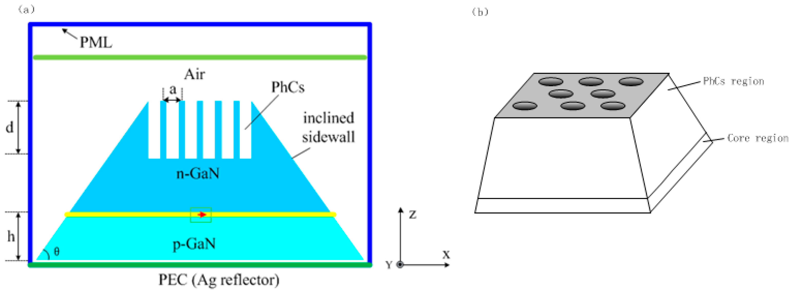
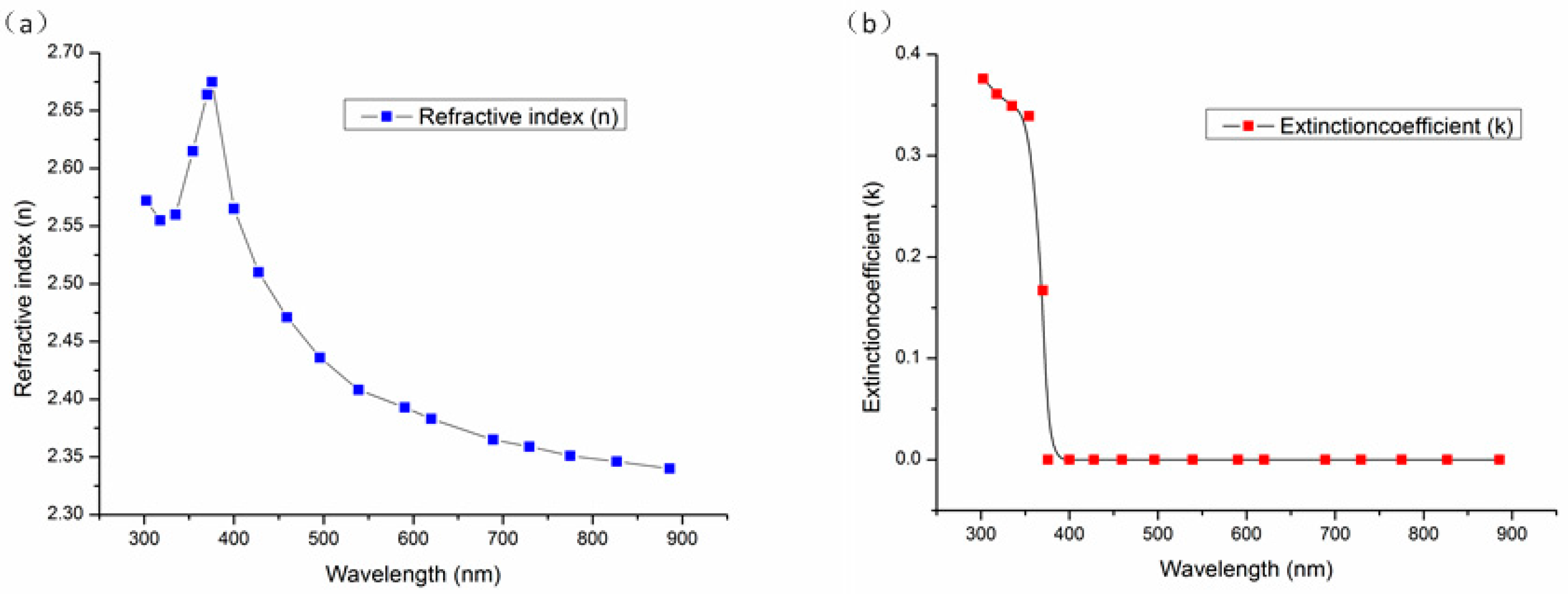
2. Device Structure and Numerical Method

Figure 1a illustrates the cross-sectional view of the inclined sidewall TFFC micro-LEDs with PhCs utilized in the FDTD simulations. Typical TFFC micro-LEDs consist of a 3 μm n-GaN layer, a 50 nm multiple-quantum-well (MQW) active layer, and a p-GaN layer on a high-reflectivity Ag reflector from top to bottom, as depicted in Figure 1 [1,21]. In this study, TFFC micro-LEDs with a square cross-section were considered, as most previously reported micro-LEDs have been manufactured in this shape. Figure 1b shows the planar scheme of the PhCs. From Figure 1b, we can see that a triangular lattice of air hole PhCs with the filling factor of
f t r i a n g l e = 2 π R 2 3 a 2
was chosen during the simulations. Here, R is the radius of the air holes, while a is the PhC period, i.e., the center-to-center distance between the neighboring PhCs [22]. To balance simulation efficiency and computational cost, the horizontal dimensions of the micro-LEDs were set at 6 μm × 6 μm. The refractive index (n) and extinction coefficient (k) of GaN used in the simulations across the entire visible emission wavelength are presented in Figure 2 [23]. The MQW active region was represented as a uniform medium with a complex effective refractive index of 2.48 + i7.32 × 10−5 during the simulations [24].
The entire chip was encompassed within the computational domain, with boundary conditions set as a perfectly matched layer (PML) on the top and the four sides to absorb outgoing waves and prevent electromagnetic wave reflections [25]. Additionally, a perfect electric conductor (PEC) layer was utilized to model power reflection on the bottom Ag reflector. To balance computational efficiency and results accuracy, a grid resolution of 10 nm was employed during the simulations [26]. A single dipole source was positioned at the center of the MQW active region in Figure 1 for simplicity. Previous studies have demonstrated that for micro-LEDs, the relative variance between the average LEE and the dipole at the center of the active region is less than 0.5% [18].
The spectral intensity distribution of the dipole source was assumed to follow a Gaussian line-shape function, with a peak wavelength of 460 nm. The analysis focused only on the x direction of the dipole source due to the predominant polarization of light emitted by InGaN MQWs parallel to the MQW plane, rendering the contribution of light polarized in the z direction negligible [27]. Previous studies have demonstrated that the LEEs of E//x and E//y polarized micro-LEDs are nearly indistinguishable. Therefore, for the subsequent simulation, an E//x polarized dipole in the xy-plane was selected as the radiating source for the micro-LEDs [28].
To assess LEE, the source power was computed within a small box encompassing the dipole. The extraction power was measured using the power monitor positioned at a distance of 460 nm from the top surface of TFFC micro-LEDs, as illustrated by the light green line in Figure 1 [18]. Subsequently, LEE was calculated as the ratio of extraction power ( P o u t ) to source power ( P s o u r c e ) [9].
η e x t r = P o u t / P s o u r c e

3. Results and Discussion

The LEE of micro-LEDs is significantly impacted by their structural parameters [18]. To elucidate the underlying physical mechanisms, an analysis was conducted to investigate how the structural parameters of micro-LEDs affect LEE through 3D FDTD simulations. Initially, a stack structure of inclined sidewall GaN-based TFFC micro-LEDs was created, and the effect of parameters such as p-GaN thickness and inclined sidewall angle on LEE was quantitatively assessed to achieve an initial optimization of GaN-based TFFC micro-LEDs. Wiesmann showed that the principles of shallow-etched PhCs on the surface of waveguides can be described as the diffraction process which can overcome total internal reflection and prevent lateral propagation of the optical waveguide [13]. In our previous research [28], the mechanisms of PhCs effectively improving the LEE were systematically investigated. Therefore, subsequently, LEE was further improved by incorporating the top PhCs, and the effect of parameters such as PhC period, filling factor, and depth on improved LEE was examined. Each parameter was varied individually during the simulations, while keeping the other parameters constant, followed by the calculation of LEE.

3.1. Effect of p-GaN Layer Thickness (h) on LEE of TFFC Micro-LEDs

According to the microcavity theory [29], the configuration in TFFC micro-LEDs positioned between the bottom Ag reflector and the top surface of n-GaN forms an optical cavity where optical resonances occur. The light-emission intensity from an embedded light source is controlled by the two factors of the Airy function and the anti-node behavior caused by the optical cavity effects. The p-GaN layer in TFFC micro-LEDs is typically thin compared to the n-GaN layer, resulting in a short distance between MQWs and the bottom Ag reflector. The anti-node factor is controlled by the position of the active layers relative to the bottom Ag reflector, which governs the coupling efficiency of the light source in guided modes, and the light emission of planar TFFC LEDs is modulated by the Fabry–Pérot effect [30]. Consequently, the thickness of the p-GaN layer h significantly impacts the interference field, light intensity distribution, radiation pattern, and LEE of TFFC micro-LEDs [30,31,32]. Therefore, the LEE of conventional planar TFFC micro-LEDs with different h was initially computed. Subsequently, this dependency was examined based on the light intensity distribution in TFFC micro-LEDs [18].
Figure 3 depicts the effect of h on the LEE of planar TFFC micro-LEDs. The LEE demonstrates oscillatory variations as h increases from 50 nm to 250 nm, as shown in Figure 3, aligning well with the findings of Ryu et al. [33]. The first two peaks of LEE are observed at h of 110 nm and 190 nm, respectively. This periodic behavior results from the interference between the upward-emitted light and the light reflected by the bottom Ag reflector [30,32]. The periodicity of h, approximately 80 nm (Figure 3), is highly consistent with the theoretical expectations for microcavity LEDs [29]. Peaks or valleys in LEE occur when constructive or destructive interference is present between the upward-emitted light and the light reflected by the bottom Ag reflector. The optimal LEE (~13.8%) observed in TFFC micro-LEDs with an h of 110 nm can be attributed to the vertical resonant condition for the highest reflection occurring around this specific value of h.
FDTD simulation results indicate that the EQE in TFFC micro-LEDs follows a pattern akin to dampened vibration with an increase in h. The variation in LEE can be attributed to the significant impact of h on the distribution of light intensity [18]. Therefore, to investigate the effect of h on LEE, the light intensity distribution of TFFC micro-LEDs was computed. Figure 4 illustrates the light intensity distributions for an h of 50 nm, 110 nm, and 200 nm, respectively.
In Figure 4, for h = 50 nm, the light intensity distribution appears uniform but weak. In contrast, for h = 200 nm, the micro-LEDs exhibit a smaller spot size with stronger central luminous intensity, resulting in a higher LEE. At h = 110 nm, both the central light intensity and spot size experience significant improvement, leading to the highest achievable LEE.

3.2. Effect of Inclined Sidewall Angle (θ) on the LEE of TFFC Micro-LEDs

The manipulation of the sidewall angle of micro-LEDs has been recognized as a method to alter the light propagation path, thereby improving LEE into the escape cone. An inclined sidewall can be effectively obtained through a chlorine-based GaN dry etch [34] or wet etch [35]. However, the use of trapezoidal chip etching techniques may result in the loss of the active layer and a subsequent reduction in IQE. To mitigate this issue, this study maintained θ within the range of 0° to 40°, with increments of 2°. Subsequently, the effect of θ on the LEE of TFFC micro-LEDs was investigated. The results are presented in Figure 5.
In Figure 5, the output power is greater for TFFC micro-LEDs with an inclined sidewall, attributed to the improved LEE. For θ < 16°, the LEE remains relatively constant. With a further increase in the angle, LEE also increases, reaching 15.43% at θ = 28°. However, a continued increase in θ results in a decrease in LEE. This observation aligns well with the findings in Lan et al. [7].
To elucidate the results, the electric field intensity profile in the steady state for planar LEDs and TFFC micro-LEDs with a θ of 28° and 40° is presented in Figure 6. This shows that, for planar TFFC micro-LEDs with θ of 0°, significant light leakage occurs at the side, leading to reduced efficiency. When θ is increased to 28°, the sidewalls effectively reflect light, redirecting it to be re-emitted from the top, thereby improving LEE. However, at a θ of 40°, excessive side light leakage is observed, which compromises efficiency. The results indicate that as θ increases, more photons undergo total internal reflection (TIR) at the sidewall, contributing to a higher LEE. However, when θ exceeds 28°, the reflected light increasingly propagates toward the chip edge, thereby reducing the overall photon collection from the top surface. Additionally, the light propagating towards the edge might go through multiple reflections at the interfaces, resulting in a lower LEE.

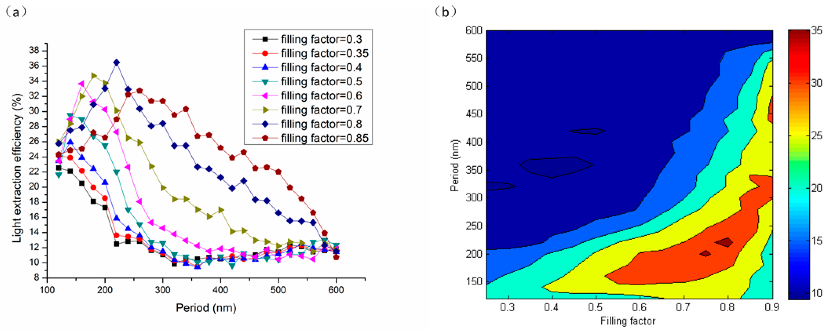
3.3. Effect of PhC Period (a) and Filling Factor (f) on the LEE of Inclined Sidewall TFFC Micro-LEDs

This study simultaneously examined the effect of the PhC period (a) and filling factor (f) on the LEE of inclined sidewall TFFC micro-LEDs. These factors were closely related to each other, while the remaining parameters were held constant at the previously determined optimal values. Specifically, h was maintained at 110 nm, and θ was set at 28°. In this context, the period (a) refers to the distance between neighboring PhC centers. The improvement in LEE, represented as a function of a and f, is depicted in Figure 7, in which a ranges from 120 nm to 600 nm, while f varies between 0.3 and 0.85.
In Figure 7a, LEE follows a consistent pattern as a and f of PhCs vary within a specific range. For PhCs with a different f, LEE initially increases to a peak value and then decreases as f increases. In Figure 7b, the optimal range for LEE is between 100 nm and 300 nm for a and between 0.5 and 0.85 for f. The highest LEE of 36.47% is achieved when f is 0.8 and a is 220 nm. As we know, if the total thickness of LEDs is so thin that there exists only one guided mode, a high LEE will be expected when the period corresponds to the second-order grating condition, λ n (a ≈ 184 nm). However, high LEE is demonstrated at relatively larger periods, i.e., 220 nm. This is because of the efficient diffraction of higher-order modes, which have higher diffraction efficiency than low-order ones [36]. Furthermore, the PhC layer can be approximated by a homogenous layer with an effective refractive index given by [37]
n P h C s = f n a i r 2 + ( 1 f ) n G a N 2
So, when the f equals 0.8, the effective refractive index of the PhC layer is about 1.42, which enables the refractive index to gradually decrease from n G a N = 2.47 to n P h C s = 1.42 and then to n a i r = 1 , which means that a graded index anti-reflection layer structure is formed between three layers, which can effectively inhibit Fresnel reflection and obtain a higher LEE [38].
To elucidate these results, the power distribution patterns of inclined sidewall TFFC micro-LEDs with varying a and f were calculated using the FDTD method (Figure 8).
Figure 8 illustrates that the power intensity pattern of light emission in inclined sidewall TFFC micro-LEDs varies significantly across different PhC configurations. Notably, when a is 220 nm and f is 0.8, a substantially larger intensity pattern is observed, attributed to the strong coupling effect of guided modes by PhCs. These simulation results confirm that the photon escape probability can be effectively enhanced by the surface PhCs’ structure. In an experiment, PhCs’ structure can be fabricated by means of polystyrene nanosphere lithography and reactive ion etching techniques [39].

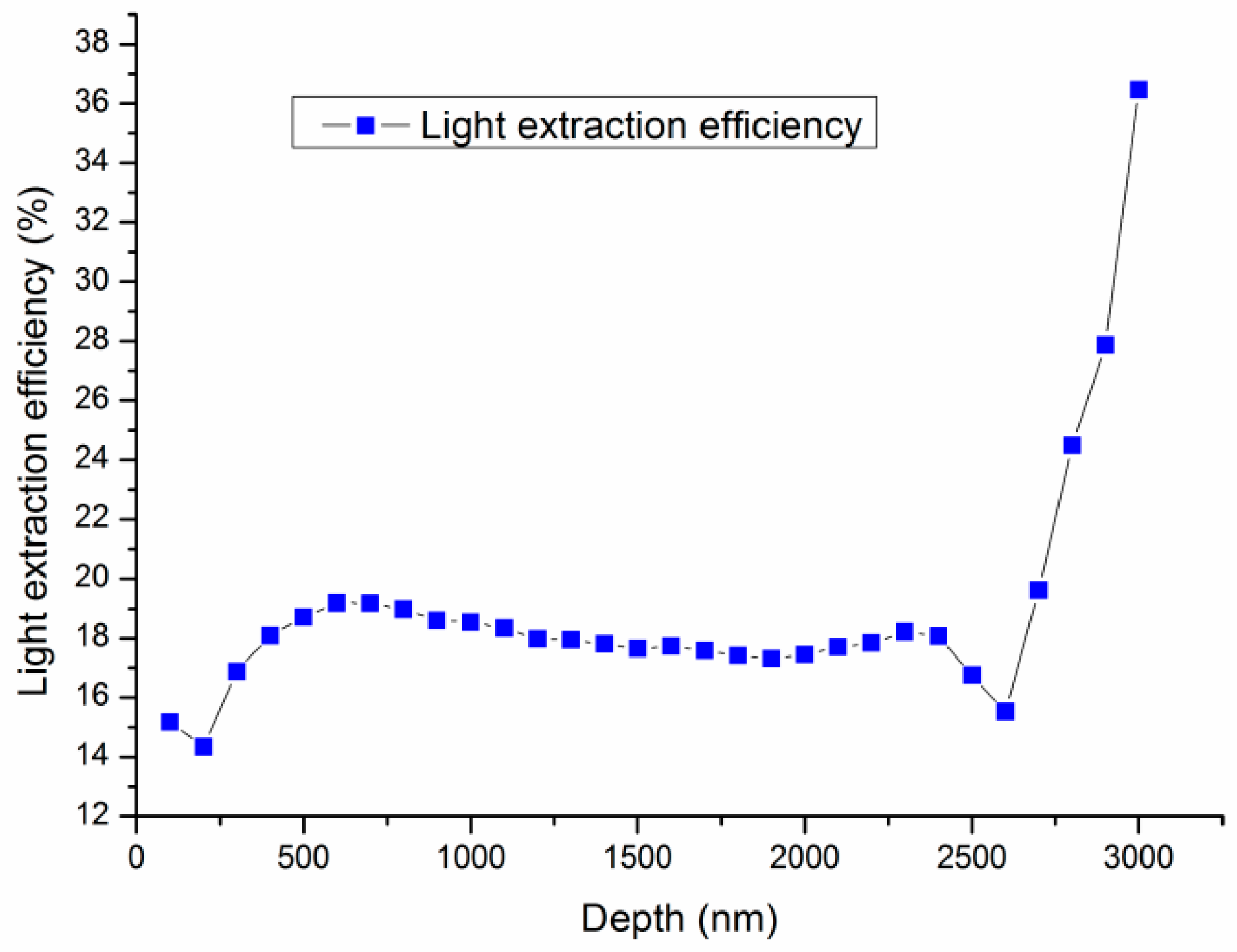
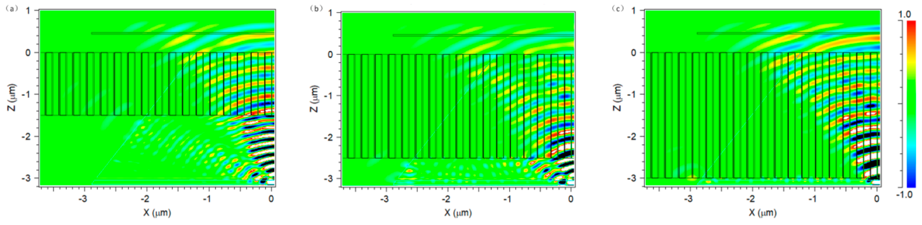
3.4. Effect of PhCs’ Hole Depth (d) on the LEE of Inclined Sidewall TFFC Micro-LEDs

This study investigated the effect of d on LEE. The simulation was conducted with and a of 220 nm and an f of 0.8, as determined previously. Figure 9 illustrates the variation in LEE with different d, ranging from 100 nm to 3000 nm in increments of 100 nm.
For values of d below 2600 nm (Figure 9), LEE remains relatively stable. This may be because when the etching depth is shallow, the distance between the PhCs and the active layer is longer, having less influence on the diffraction of the optical waveguide mode. However, as d surpasses this threshold, there is a significant increase in LEE. Specifically, at d = 3000 nm, the extraction efficiency peaks at 36.47%. This behavior can be attributed to the heightened diffraction effect of PhCs as their depth increases, leading to a greater number of diffracted guided modes. Moreover, in consideration of the theoretical synergistic effect between the inclined sidewall and PhCs in the improvement of LEE, the light reflected from the sidewall can be diffracted by directly interacting with the PhCs without the reflection from the bottom Ag reflector and then emitted from the surface of the LEDs, which can effectively improve the LEE. This trend is further supported by the variations in electric field intensity of the micro-LEDs with different d values of 1500 nm, 2500 nm, and 3000 nm (Figure 10).
Figure 10 shows that when d is 1500 nm or 2500 nm, a greater portion of the power is confined between PhCs and the bottom Ag reflector, resulting in reduced power traveling towards the top of the micro-LEDs. However, at d of 3000 nm, a significant increase in emitted light is observed, indicating that the diffraction effect is strongest at d. These simulation results align well with the findings reported in Wei et al. [40].
It should be pointed out that when we etch PhCs, we try not to cross the active layer. Although deep-etched PhCs through the active layer can enhance the interaction between guided modes and PhCs, this will also decrease the IQE of the devices and cause a significant reduction in the radiative recombination rate as the photon density of states is heavily reduced [13]. Therefore, here, we mainly study the case where the PhCs does not penetrate the active layer—that is, the etching depth is less than 3000 nm.

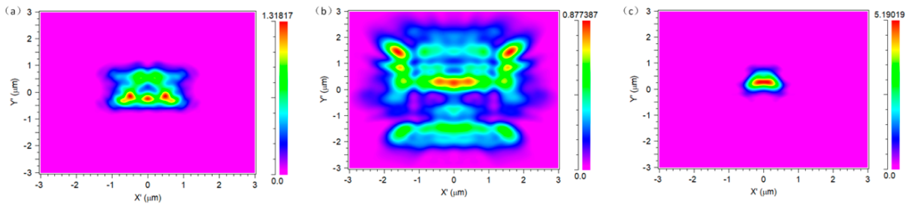
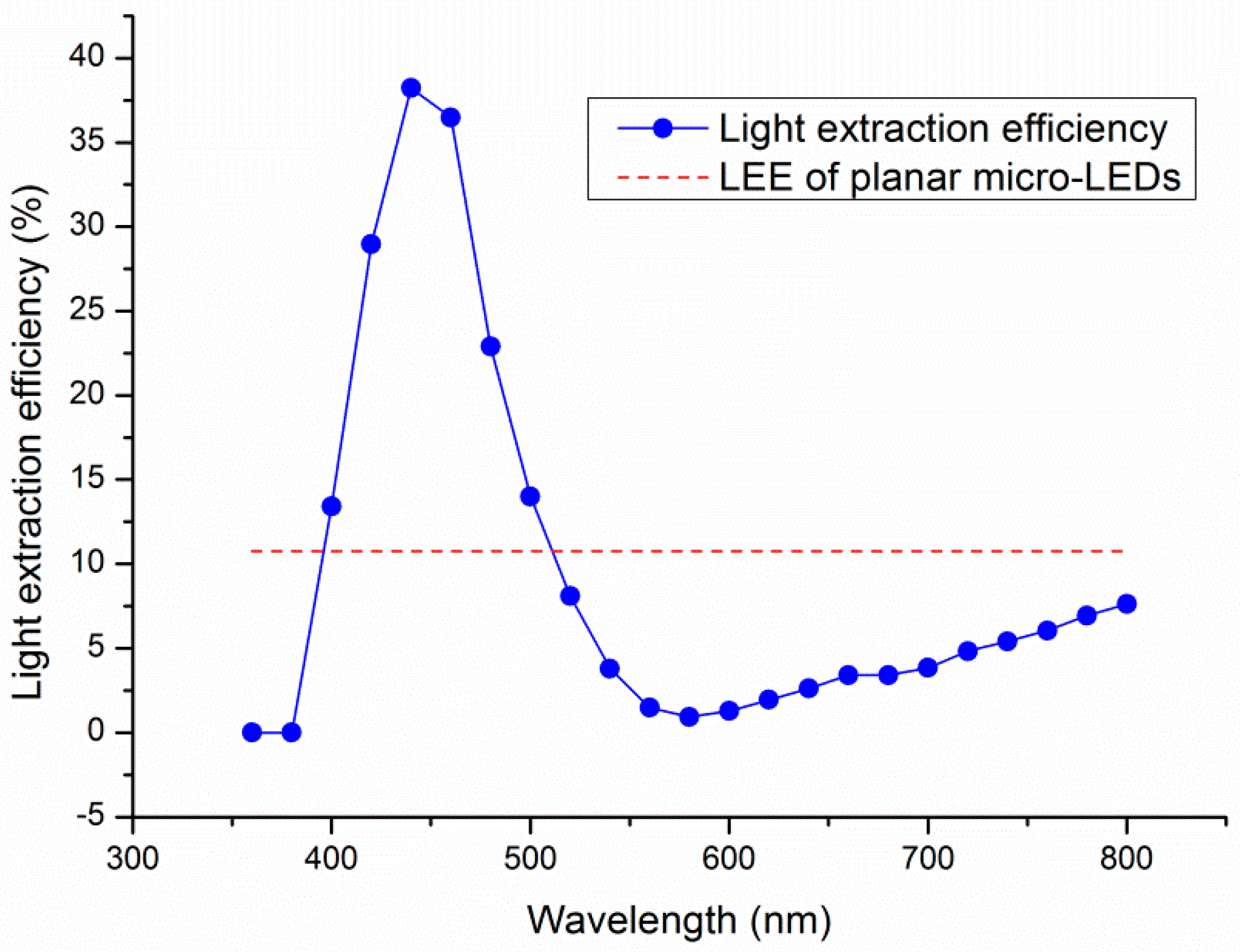
3.5. The LEE over the Whole Visible Spectrum

An investigation was conducted on the LEE of TFFC micro-LEDs with PhCs across the entire visible spectrum. Figure 11 illustrates LEE relative to the emission source wavelength. The results in Figure 11 indicate that TFFC micro-LEDs with PhCs exhibited a higher LEE compared to conventional planar LEDs within the wavelength range of 400 nm to 500 nm. The peak LEE was observed at 460 nm, corresponding to blue light, which was attributed to GaN.

4. Conclusions

This study employed a combination of an inclined sidewall and PhCs to improve the LEE of GaN-based TFFC micro-LEDs. The effects of key parameters, including h, θ, f, a, and d, on the LEE of TFFC micro-LEDs were analyzed using 3D FDTD simulations. Optimization resulted in a maximum LEE of 36.47%, achieved with an h of 110 nm, a θ of 28°, and PhCs with a d of 3000 nm, an a of 220 nm, and an f of 0.8. This configuration led to a 238.5% improvement in LEE compared to conventional planar TFFC micro-LEDs, primarily due to the synergistic of the reflection effect of the bottom Ag reflector and the inclined sidewall along with the diffraction effect of PhCs. These results provide valuable insights and practical guidelines for the design and fabrication of high-efficiency GaN-based micro-LEDs.

Author Contributions

Conceptualization, M.L.; simulation, M.L., and X.Z.; results, analysis X.Z.; writing—original draft preparation, M.L.; writing—review and editing, X.Z. All authors have read and agreed to the published version of the manuscript.

Funding

This research was funded by the Project of Shandong Province Higher Educational Science and Technology Program in China, grant number J17KA054.

Data Availability Statement

The original contributions presented in the study are included in the article, further inquiries can be directed to the corresponding author.

Conflicts of Interest

The authors declare no conflicts of interest.

References

  1. González-Izquierdo, P.; Rochat, N.V.; Zoccarato, D.; Rol, F.; Simon, J.; Le Maitre, P.; Volpert, M.; Charles, M.; Lafossas, M.; Torrengo, S. Influence of shape and size on GaN/InGaN μLED light emission: A competition between sidewall defects and light extraction efficiency. ACS Photonics 2023, 10, 4031–4037. [Google Scholar] [CrossRef]
  2. Hang, S.; Chuang, C.-M.; Zhang, Y.; Chu, C.; Tian, K.; Zheng, Q.; Wu, T.; Liu, Z.; Zhang, Z.-H.; Li, Q. A review on the low external quantum efficiency and the remedies for GaN-based micro-LEDs. J. Phys. D Appl. Phys. 2021, 54, 153002. [Google Scholar] [CrossRef]
  3. Tian, M.; Yu, H.; Memon, M.H.; Xing, Z.; Huang, C.; Jia, H.; Zhang, H.; Wang, D.; Fang, S.; Sun, H. Enhanced light extraction of the deep-ultraviolet micro-LED via rational design of chip sidewall. Opt. Lett. 2021, 46, 4809–4812. [Google Scholar] [CrossRef] [PubMed]
  4. Gardner, N.; Müller, G.; Shen, Y.; Chen, G.; Watanabe, S.; Götz, W.; Krames, M. Blue-emitting InGaN–GaN double-heterostructure light-emitting diodes reaching maximum quantum efficiency above 200A∕cm2. Appl. Phys. Lett. 2007, 91, 243506. [Google Scholar] [CrossRef]
  5. Gan, Z.; Wen, X.; Chen, W.; Zhou, C.; Yang, S.; Cao, G.; Ghiggino, K.P.; Zhang, H.; Jia, B. The dominant energy transport pathway in halide perovskites: Photon recycling or carrier diffusion? Adv. Energy Mater. 2019, 9, 1900185. [Google Scholar] [CrossRef]
  6. Cao, Y.; Wang, N.; Tian, H.; Guo, J.; Wei, Y.; Chen, H.; Miao, Y.; Zou, W.; Pan, K.; He, Y. Perovskite light-emitting diodes based on spontaneously formed submicrometre-scale structures. Nature 2018, 562, 249–253. [Google Scholar] [CrossRef]
  7. Lan, S.; Wan, H.; Zhao, J.; Zhou, S. Light extraction analysis of AlGaInP based red and GaN based blue/green flip-chip micro-LEDs using the monte carlo ray tracing method. Micromachines 2019, 10, 860. [Google Scholar] [CrossRef]
  8. Lee, T.-Y.; Chen, L.-Y.; Lo, Y.-Y.; Swayamprabha, S.S.; Kumar, A.; Huang, Y.-M.; Chen, S.-C.; Zan, H.-W.; Chen, F.-C.; Horng, R.-H. Technology and applications of micro-LEDs: Their characteristics, fabrication, advancement, and challenges. ACS Photonics 2022, 9, 2905–2930. [Google Scholar] [CrossRef]
  9. Wang, H.; Wang, L.; Sun, J.; Guo, T.-L.; Chen, E.-G.; Zhou, X.-T.; Zhang, Y.-A.; Yan, Q. Role of surface microstructure and shape on light extraction efficiency enhancement of GaN micro-LEDs: A numerical simulation study. Displays 2022, 73, 102172. [Google Scholar] [CrossRef]
  10. Bulashevich, K.A.; Konoplev, S.S.; Karpov, S.Y. Effect of die shape and size on performance of III-nitride micro-LEDs: A modeling study. Photonics 2018, 5, 41. [Google Scholar] [CrossRef]
  11. Kang, K.; Yoon, J.; Kim, J.; Lee, H.; Yang, B. Effect of the finite pixel boundary on the angular emission characteristics of top-emitting organic light-emitting diodes. Opt. Express 2015, 23, A709–A717. [Google Scholar] [CrossRef] [PubMed]
  12. Gou, F.; Hsiang, E.-L.; Tan, G.; Chou, P.-T.; Li, Y.-L.; Lan, Y.-F.; Wu, S.-T. Angular color shift of micro-LED displays. Opt. Express 2019, 27, A746–A757. [Google Scholar] [CrossRef] [PubMed]
  13. Wiesmann, C.; Bergenek, K.; Linder, N.; Schwarz, U.T. Photonic crystal LEDs–designing light extraction. Laser Photonics Rev. 2009, 3, 262–286. [Google Scholar] [CrossRef]
  14. Yuan, S.; Zhang, X.; Cao, W.; Sheng, Y.; Liu, C.; Yu, L.; Di, Y.; Chen, Z.; Dong, L.; Gan, Z. Fluorescence enhancement of perovskite nanocrystals using photonic crystals. J. Mater. Chem. C 2021, 9, 908–915. [Google Scholar] [CrossRef]
  15. Yuan, S.; Sheng, Y.; Liu, C.; Yu, L.; Dong, L.; Xing, F.; Zhang, J.; Di, Y.; Gan, Z. Fluorescence enhancement of perovskite nanocrystals by flexible photonic crystals and its application in optical strain gauge. Appl. Phys. Lett. 2021, 119, 033302. [Google Scholar] [CrossRef]
  16. Li, S.-H.; Lin, C.-P.; Fang, Y.-H.; Kuo, W.-H.; Wu, M.-H.; Chao, C.-L.; Horng, R.-H.; Su, G.-D.J. Performance analysis of GaN-based micro light-emitting diodes by laser lift-off process. Solid State Electron. Lett. 2019, 1, 58–63. [Google Scholar] [CrossRef]
  17. Wang, L.; Sun, J.; Yan, Q.; Lin, J.; Guo, W.; Chen, E.; Xu, C.; Liu, Y. Issue of spatial coherence in MQW based micro-LED simulation. Opt. Express 2021, 29, 31520. [Google Scholar] [CrossRef]
  18. Ryu, H.-Y.; Pyo, J.; Ryu, H.Y. Light extraction efficiency of GaN-based micro-scale light-emitting diodes investigated using finite-difference time-domain simulation. IEEE Photonics J. 2020, 12, 1–10. [Google Scholar] [CrossRef]
  19. Yu, B.; Meng, J.; Li, J.; Wu, J.; Ding, X.; Li, Z.-T. Utilizing Photothermal Actuation Structure to Improving Light Extraction Efficiency and Ambient Contrast Ratio of Light-Emitting Diode Display Devices. IEEE Trans. Electron. Devices 2024, 71, 681–688. [Google Scholar] [CrossRef]
  20. Hu, X.; Cai, J.; Ye, Y. Simulation model of GaN-based micro-LED with high light extraction efficiency. Acta Opt. Sin. 2022, 42, 1525001. [Google Scholar]
  21. Ding, Q.-a.; Li, K.; Kong, F.; Chen, X.; Zhao, J. Improving the vertical light-extraction efficiency of GaN-based thin-film flip-chip LEDs with p-side deep-hole photonic crystals. J. Disp. Technol. 2013, 10, 909–916. [Google Scholar] [CrossRef]
  22. David, A.; Meier, C.; Sharma, R.; Diana, F.S.; Denbaars, S.P.; Hu, E.; Nakamura, S.; Weisbuch, C.; Benisty, H. Photonic bands in two-dimensionally patterned multimode GaN waveguides for light extraction. Appl. Phys. Lett. 2005, 87, 101107. [Google Scholar] [CrossRef]
  23. Palik, E.D. Handbook of Optical Constants of Solids; Academic Press: Cambridge, MA, USA, 1998; Volume 3. [Google Scholar]
  24. Laws, G.; Larkins, E.; Harrison, I.; Molloy, C.; Somerford, D. Improved refractive index formulas for the AlxGa1−xN and InyGa1−yN alloys. J. Appl. Phys. 2001, 89, 1108–1115. [Google Scholar] [CrossRef]
  25. Sacks, Z.S.; Kingsland, D.M.; Lee, R.; Lee, J.-F. A perfectly matched anisotropic absorber for use as an absorbing boundary condition. IEEE Trans. Antennas Propag. 1995, 43, 1460–1463. [Google Scholar] [CrossRef]
  26. Liu, M.; Li, K.; Kong, F.-M.; Zhao, J.; Zhao, S.-L.; Meng, H.-T. Analysis of the light-extraction efficiency of SiC substrate-based flip-chip vertical light-emitting diodes with embedded photonic crystals. Jpn. J. Appl. Phys. 2016, 55, 112101. [Google Scholar] [CrossRef]
  27. David, A. High-Efficiency GaN-Based Light-Emitting Diodes: Light Extraction by Photonic Crystals and Microcavities. Ecole Polytechnique X. 2006. Available online: https://pastel.hal.science/pastel-00002956/ (accessed on 18 September 2024).
  28. Liu, M.; Li, K.; Kong, F.-M.; Zhao, J.; Yue, Q.-Y.; Yu, X.-J. Enhanced light-extraction efficiency of GaN-based light-emitting diodes with hybrid photonic crystals. Opt. Quantum Electron. 2015, 47, 2593–2604. [Google Scholar] [CrossRef]
  29. Benisty, H.; Neve, H.D.; Weisbuch, C. Impact of planar microcavity effects on light extraction—Part I: Basic concepts and analytical trends. IEEE J. Quantum Electron. 1998, 34, 1612–1631. [Google Scholar] [CrossRef]
  30. Shen, Y.; Wierer, J.; Krames, M.; Ludowise, M.; Misra, M.; Ahmed, F.; Kim, A.; Mueller, G.; Bhat, J.; Stockman, S. Optical cavity effects in InGaN/GaN quantum-well-heterostructure flip-chip light-emitting diodes. Appl. Phys. Lett. 2003, 82, 2221–2223. [Google Scholar] [CrossRef]
  31. Li, S.; Shen, M.-C.; Lai, S.; Dai, Y.; Chen, J.; Zheng, L.; Zhu, L.; Chen, G.; Lin, S.-H.; Peng, K.-W. Impacts of p-GaN layer thickness on the photoelectric and thermal performance of AlGaN-based deep-UV LEDs. Opt. Express 2023, 31, 36547–36556. [Google Scholar] [CrossRef]
  32. Ryu, H.-Y.; Shim, J.-I. Structural parameter dependence of light extraction efficiency in photonic crystal InGaN vertical light-emitting diode structures. IEEE J. Quantum Electron. 2010, 46, 714–720. [Google Scholar]
  33. Ryu, H.-Y.; Choi, I.-G.; Choi, H.-S.; Shim, J.-I. Investigation of Light Extraction Efficiency in AlGaN Deep-Ultraviolet Light-Emitting Diodes. Appl. Phys. Express 2013, 6, 062101. [Google Scholar] [CrossRef]
  34. Hahn, H.; Gruis, J.B.; Ketteniss, N.; Urbain, F.; Kalisch, H.; Vescan, A. Influence of mask material and process parameters on etch angle in a chlorine-based GaN dry etch. J. Vac. Sci. Technol. A 2012, 30, 051302. [Google Scholar] [CrossRef]
  35. Yue, Y.; Yan, X.; Li, W.; Xing, H.G.; Jena, D.; Fay, P. Faceted sidewall etching of n-GaN on sapphire by photoelectrochemical wet processing. J. Vac. Sci. Technol. B 2014, 32, 061201. [Google Scholar] [CrossRef]
  36. Orita, K.; Tamura, S.; Takizawa, T.; Ueda, T.; Yuri, M.; Takigawa, S.; Ueda, D. High-extraction-efficiency blue light-emitting diode using extended-pitch photonic crystal. Jpn. J. Appl. Phys. 2004, 43, 5809. [Google Scholar] [CrossRef]
  37. de Nazareth Matioli, E. Embedded Photonic Crystals for High-Efficiency Gallium Nitride-Based Optoelectronic Devices; University of California: Santa Barbara, CA, USA, 2010. [Google Scholar]
  38. Zhu, J.; Yu, Z.; Burkhard, G.F.; Hsu, C.-M.; Connor, S.T.; Xu, Y.; Wang, Q.; McGehee, M.; Fan, S.; Cui, Y. Optical absorption enhancement in amorphous silicon nanowire and nanocone arrays. Nano Lett. 2009, 9, 279–282. [Google Scholar] [CrossRef]
  39. Fu, P.-H.; Lin, G.-J.; Wang, H.-P.; Lai, K.-Y.; He, J.-H. Enhanced light extraction of light-emitting diodes via nano-honeycomb photonic crystals. Nano Energy 2014, 8, 78–83. [Google Scholar] [CrossRef]
  40. Wei, T.; Ji, X.; Wu, K.; Zheng, H.; Du, C.; Chen, Y.; Yan, Q.; Zhao, L.; Zhou, Z.; Wang, J.; et al. Efficiency improvement and droop behavior in nanospherical-lens lithographically patterned bottom and top photonic crystal InGaN/GaN light-emitting diodes. Opt. Lett. 2014, 39, 379. [Google Scholar] [CrossRef]
Figure 1. (a) Cross-sectional schematic of inclined sidewall TFFC micro-LEDs with PhCs. Θ is the angle between the inclined sidewall and the horizontal direction. The dipole source is represented by the red arrow in this figure and the small light green box encompassing the dipole represents the source power monitor, while the extraction power monitor is illustrated by the light green line positioned at a certain distance of 460 nm from the top surface of TFFC micro-LEDs. (b) The planar scheme of the PhCs.
Electronics 13 03750 g001
Figure 2. The (a) refractive index and (b) extinction coefficient of GaN.
Electronics 13 03750 g002
Figure 3. Effect of h on LEE of TFFC micro-LEDs.
Electronics 13 03750 g003
Figure 4. Light intensity distribution in TFFC micro-LEDs for an h of (a) 50 nm, (b) 110 nm, and (c) 200 nm.
Electronics 13 03750 g004
Figure 5. Effect of θ on the LEE of TFFC micro-LEDs.
Electronics 13 03750 g005
Figure 6. Steady-state electric field intensity profile in (a) planar TFFC micro-LEDs and TFFC micro-LEDs with a θ of (b) 28° and (c) 40°.
Electronics 13 03750 g006
Figure 7. Effect of PhC period a and filling factor f on LEE: (a) curve graph; (b) 2D chromatogram.
Electronics 13 03750 g007
Figure 8. Power distribution patterns in inclined sidewall TFFC micro-LEDs with PhCs for (a) an a of 320 nm and an f of 0.35, (b) an a of 220 nm and an f of 0.8, and (c) an a of 560 nm and an f of 0.85.
Electronics 13 03750 g008
Figure 9. Effect of PhC depth d on the LEE.
Electronics 13 03750 g009
Figure 10. Steady-state electric field intensity profile in TFFC micro-LEDs with a d of (a) 1500 nm, (b) 2500 nm, and (c) 3000 nm.
Electronics 13 03750 g010
Figure 11. LEE across the visible spectrum.
Electronics 13 03750 g011
Table 1. Comparison between previous research results and this work.
MethodLEE Enhancement
Photothermal actuation structure [19]150%
Surface grating [9]200%
Distributed Bragg reflectors [20]242%
This work238.5%
Disclaimer/Publisher’s Note: The statements, opinions and data contained in all publications are solely those of the individual author(s) and contributor(s) and not of MDPI and/or the editor(s). MDPI and/or the editor(s) disclaim responsibility for any injury to people or property resulting from any ideas, methods, instructions or products referred to in the content.

