Article

Modeling, Design, and Application of Analog Pre-Distortion for the Linearity and Efficiency Enhancement of a K-Band Power Amplifier

1
Department of Electrical and Computer Engineering, Villanova University, Villanova, PA 19085, USA
2
Department of Electrical & Electronic Engineering, University of Bristol, Bristol BS8 1QU, UK
3
Filtronic PLC, Stockton-on-Tees TS21 3FD, UK
4
School of Electronic and Electrical Engineering, University of Leeds, Leeds LS2 9JT, UK
*
Author to whom correspondence should be addressed.
Electronics 2024, 13(19), 3818; https://doi.org/10.3390/electronics13193818
Submission received: 2 September 2024 / Revised: 18 September 2024 / Accepted: 22 September 2024 / Published: 27 September 2024

Abstract

:
This paper presents the theory, design, and application of a dual-branch series-diode analog pre-distortion (APD) linearizer to improve the linearity and efficiency of a K-band high-power amplifier (HPA). A first-of-its-kind, frequency-dependent large-signal APD model is presented. This model is used to evaluate different phase relationships between the linear and nonlinear branches, suggesting independent gain and phase expansion characteristics with this topology. This model is used to assess the impact of diode resistance, capacitance, and ideality factors on the APD characteristics. This feature is showcased with two similar GaAs diodes to find the best fit for the considered HPA. The selected diode is characterized and modeled between 1 and 26.5 GHz. A comprehensive APD design and simulation workflow is reported. Before fabrication, the simulated APD is evaluated with the measured HPA to verify linearity improvements. The APD prototype achieves a large-signal bandwidth of 6 GHz with 3 dB gain expansion and 8° phase rotation. This linearizer is demonstrated with a 17–21 GHz GaN HPA with 41 dBm output power and 35% efficiency. Using a wideband 750 MHz signal, this APD improves the noise–power ratio (NPR) by 6.5–8.2 dB over the whole HPA bandwidth. Next, the HPA output power is swept to compare APD vs. power backoff for the same NPR. APD improves the HPA output power by 1–2 W and efficiency by approximately 5–9% at 19 GHz. This efficiency improvement decreases by only 1–2% when including the APD post-amplifier consumption, thus suggesting overall efficiency and output power improvements with APD at K-band frequencies.

1. Introduction

Attaining amplification with high power, efficiency, and linearity on a wide frequency range poses a formidable challenge, particularly when operating at higher frequencies. Pre-distortion linearization is an effective technique that can be introduced before the high-power amplifier (HPA) to compensate for the HPA nonlinear characteristics in both amplitude and phase over its bandwidth [1]. This can be easily achieved at baseband with digital pre-distortion (DPD), thanks to the high flexibility of digital algorithms. However, DPD requires the use of digital signal processors such as FPGAs or ASICs whose cost and power consumption increase with the clock frequency [2]. DPD also requires the use of at least five times the signal bandwidth, thus significantly increasing the power demand of the digital baseband [2].
Analog pre-distortion (APD) linearization has a fundamental advantage over DPD by directly implementing the APD circuit in the RF/microwave front-end with minimal addition of hardware, cost, and power consumption while enabling very wide bandwidths. It is, therefore, an ideal technique for many fields, such as wideband RF transmitters, radio-over-fiber-optic, satellite communications, radar, and electronic warfare systems. The linearizer module is typically composed of an APD circuit, including a nonlinearity or inter-modulation generator and a post-amplifier that compensates for the losses of the analog linearizer.
The degree of improvement attainable with APD depends on the HPA compression point [1]. At deep compression, the HPA is clipping, and both DPD and APD cannot recover from this. When instead the HPA is in backoff, APD linearization is unnecessary and may even degrade HPA linearity [1]. When instead the HPA is operated 3–4 dB into compression, to maximize its output power and efficiency, APD linearization is an effective technique that can increase the HPA linearity.
APD is particularly suitable with HPAs realized with Gallium-Nitride (GaN) as they can provide wide bandwidths that are difficult to cover with DPD. GaN is also a well-suited technology for space and satellite applications, given its radiation hardness and temperature handling capabilities. Today, commercial mm-wave GaN HPAs can achieve 10 W output power with up to 35% efficiencies and bandwidths exceeding 4 GHz at K-band, e.g., [3]. However, such efficiencies rapidly decrease when the HPA is operated in backoff to improve linearity.
APD linearizer architectures can be divided into (1) single-branch linearizers and (2) dual-branch linearizers [4]. Both (1) and (2) rely on a nonlinearity generator, either an amplifier or a diode. For best performance, this nonlinearity needs to closely match the HPA compression shaping in amplitude and phase.
Single-branch linearizers can be based on a shunt diode [5,6], on a series diode [7], or on a FET [8] and have shown adjacent channel power ratio (ACPR) improvements between 5 and 7 dB. Important design parameters of single-branch APDs are the diode parallel capacitor and the bias point. By tuning the diode bias and parallel capacitor value, it is possible to improve the HPA linearity but with ACPR improvements below 4 dB [4]. A single-branch shunt diode linearizer at 2.4 GHz achieves improvements of the ACPR of 5 dB and improvement of the HPA efficiency by 8.5% [5]. This concept is extended in [6] using two shunt diodes separated by a transmission line to achieve higher suppression at 2.2–2.3 GHz. At Ku-band frequencies (14–15 GHz), a single-branch linearizer based on a branch-line hybrid has been demonstrated to achieve up to 11 dB gain expansion and 180° phase rotation [9]. At V band frequencies, a single-branch linearizer is realized with a 3 dB waveguide coupler and a pair of Schottky diodes in [10]. This linearizer provides up to 7.8 dB amplitude expansion and 28° phase expansion between 59 and 61 GHz.
Dual-branch linearizers provide higher performance as compared to single-branch linearizers thanks to the extra degree of flexibility introduced by the added branch [10,11,12,13,14,15]. Recently, a dual-branch linearizer with independently tunable gain and phase at Ka-band frequencies has been proposed in [13]. This linearizer achieves 4.5 dB gain expansion and 23.4° phase variation at 29–31 GHz [13]. At lower frequencies, a triple-diode linearizer for narrowband HPAs at 2.14 GHz is proposed in [15], and it is used to reduce dual inflection in the gain characteristic typical of high-efficiency HPA modes. This linearizer can reduce the gain expansion by 0.4 dB while maintaining the same P 1 d B and improving the IMD3 by 10 dB. Another example is the one discussed in [14] in which two diodes connected to a hybrid coupler are used to obtain a purer cubic nonlinearity. This linearizer achieves between 11.5 and 22.6 dB improvement of the IMD3 between 27 and 31 GHz.
This work advances the associated conference paper [16] by introducing a first-of-its-kind APD model of the proposed dual-branch series-diode linearizer [17]. This model is used to investigate the impact of the phase offset between the linear and nonlinear branches, highlighting the possibility of achieving negative or positive phase rotation while maintaining the same gain expansion. This model is used to compare two similar diodes to find the best fit for the inverted HPA characteristics. The selected diode is characterized between 1 and 26.5 GHz. A detailed simulation and design workflow are reported for this APD. Simulation results predict a large-signal bandwidth of 16–25 GHz with a gain expansion of 4–5 dB and phase rotation of 10 . The simulated APD is verified with the HPA-in-the-loop to evaluate linearity improvements before APD fabrication. Next, the APD circuit is experimentally characterized at small and large-signal, with results used to validate the APD model. The APD circuit archives 3 dB gain expansion and 8° phase increase between 15 and 21 GHz. This APD can increase the average output power and efficiency, including post-amplifier consumption, across the whole bandwidth of a K-band GaN HPA.

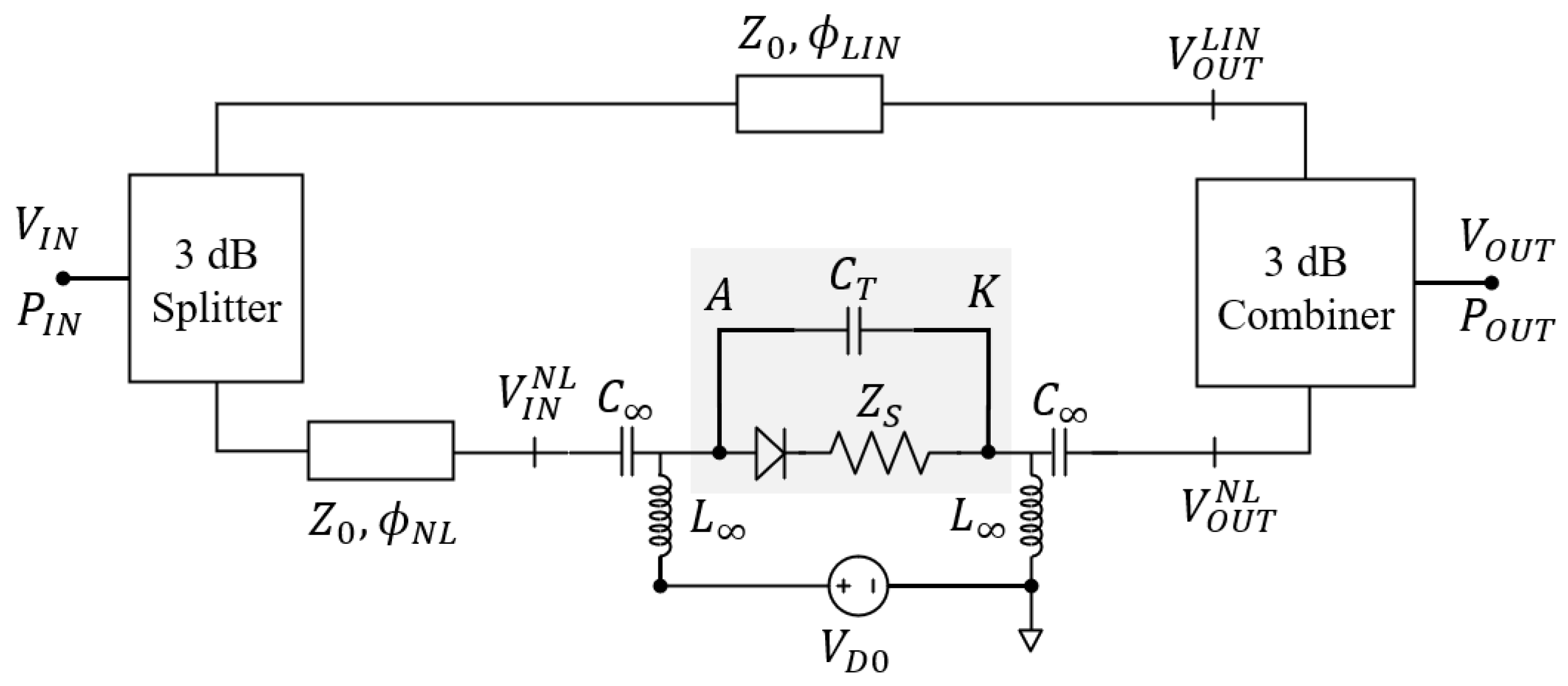
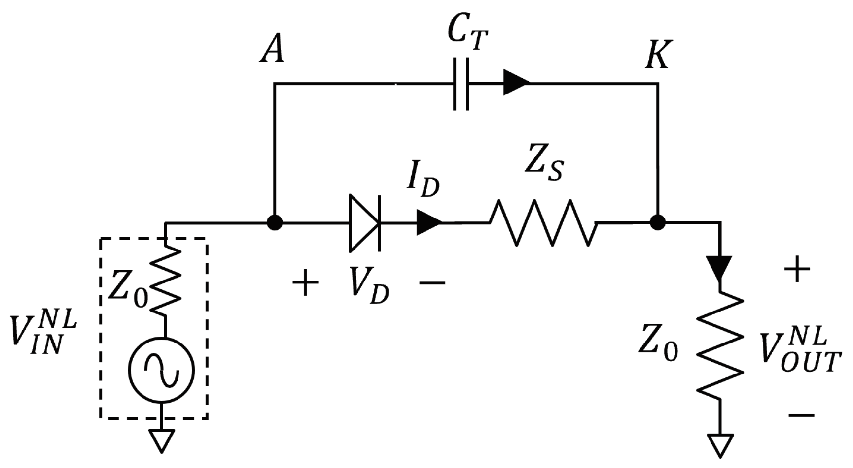
2. Wideband Large-Signal APD Model

The block diagram of the APD linearizer is shown in Figure 1. This linearizer uses a 3 dB splitter to feed a linear and a nonlinear branch. The linear branch is realized with a transmission line of electrical length ϕ L I N ( f ) . The nonlinear branch contains a line of electrical length ϕ N L ( f ) , a series diode, and two bias-Ts providing a bias voltage V D 0 . The output of the two branches is summed by a 3 dB combiner.
Let’s assume a power P I N = V I N 2 / 2 Z 0 at the APD input, where V I N is the peak RF voltage and Z 0 is the characteristic impedance. This signal is split by a lossless perfectly matched 3 dB splitter that generates two in-phase signals V I N / 2 at the input of the linear and nonlinear branches. The linear branch is modeled with an ideal lossless transmission line described by
V O U T L I N ( f ) = V I N 2 e j ϕ L I N ( f )
The nonlinear branch uses an ideal lossless transmission line to connect to the diode and bias-Ts, which is described by
V I N N L ( f ) = V I N 2 e j ϕ N L ( f )
Let us now define the phase difference Δ ϕ between the two lines (frequency dependency is suppressed for brevity)
Δ ϕ = ϕ L I N ϕ N L
For a given diode nonlinearity, the phase difference Δ ϕ sets the APD amplitude response, while ϕ L I N controls the APD phase response (as described later). Let us now consider a diode with a cut-off frequency f C much higher than the carrier frequency f 0
f C = 1 2 π R S C T > > f 0
Here, R S is the series resistance, and C T is the total capacitance at the diode extrinsic terminals (A-K) defined in Figure 1. We note that the Schottky diode used for this APD has a cut-off frequency of 663 GHz, which is much higher than the HPA upper cut-off frequency of 21 GHz.
The AC equivalent circuit of the series diode is shown in Figure 2. The current balance at the output node is
I D + V I N N L V O U T N L Z C T = V O U T N L Z 0
where Z C T = 1 / j ω C T . Thus, the output voltage is
V O U T N L = Z 0 Z 0 + Z C T V I N N L + Z 0 Z C T Z 0 + Z C T I D
The diode is described using the exponential model
I D = I S ( e α V D 1 )
Here, I S is the diode saturation current, α is q / n k T , where q is the electron charge, n is the ideality factor, k is the Boltzmann’s constant, and T is the temperature in Kelvin. No junction capacitance is included for simplicity (only the A-K linear capacitance is considered).
By substituting (7) in (6), we obtain
V O U T N L = Z 0 Z 0 + Z C T V I N N L + Z 0 Z C T Z 0 + Z C T I S ( e α V D 1 )
The diode voltage V D depends on the DC bias V D 0 and on the AC voltages and current at its terminals
V D = V D 0 + V I N N L V O U T N L Z S I D
where Z S = R S + j ω L S . By substituting (5) in (9), we have
V D = V D 0 + V I N N L 1 + Z S Z C T V O U T N L 1 + Z S Z 0 + Z S Z C T
Finally, the linear and nonlinear branches are combined using a perfectly matched, lossless combiner described by
V O U T = V O U T L I N 2 + V O U T N L 2
In summary, the dual-branch series-diode APD model of input V I N and output V O U T can be formulated as follows:
V O U T L I N = V I N 2 e j ϕ L I N , V I N N L = V I N 2 e j ϕ N L , V O U T N L = Z 0 Z 0 + Z C T V I N N L + Z 0 Z C T Z 0 + Z C T I S ( e α V D 1 ) , V D = V D 0 + 1 + Z S Z C T V I N N L 1 + Z S Z 0 + Z S Z C T V O U T N L , V O U T = V O U T L I N 2 + V O U T N L 2 .
This APD model has been solved numerically considering a maximum input power P I N , M A X = 20 dBm at the frequency f 0 = 19 GHz (unless specified otherwise). The considered diode parameters are I S = 0.2 pA, C T = 40 fF, R S = 6 Ω , n = 1.2 , and T = 300 K (thus α = 32.2 V 1 ).

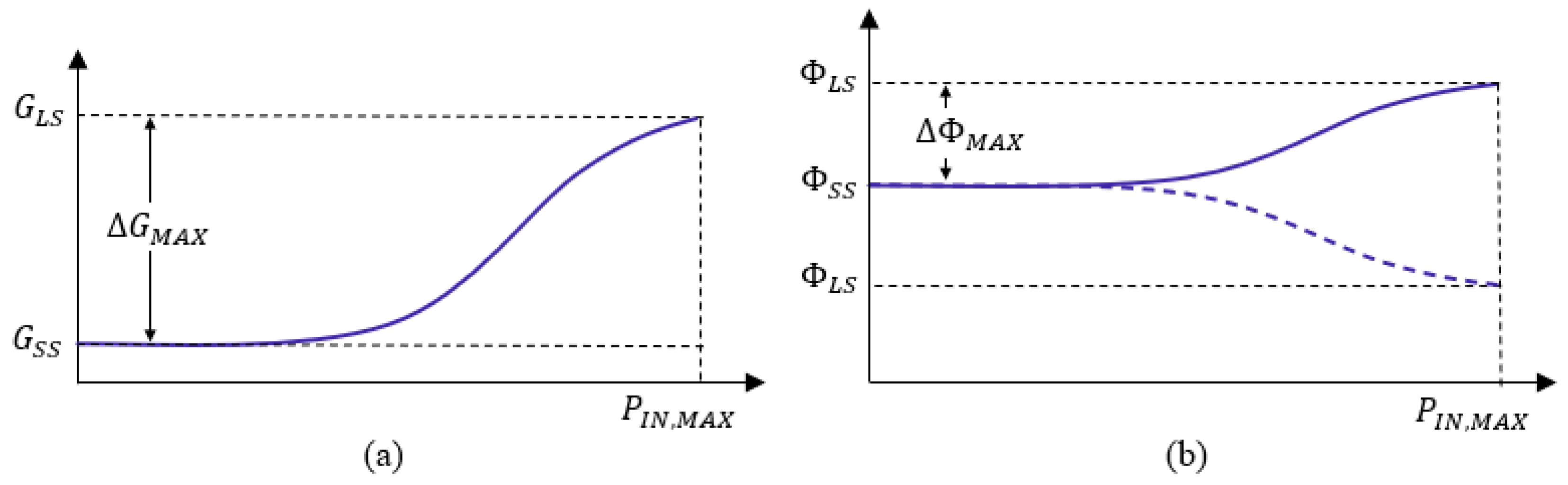
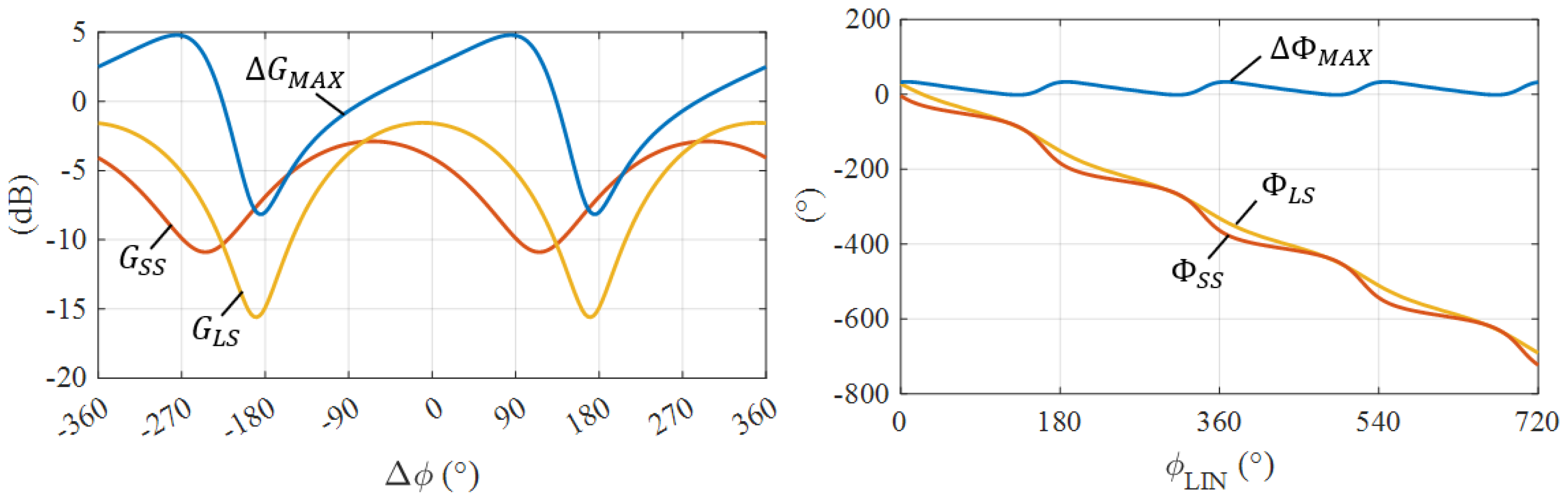
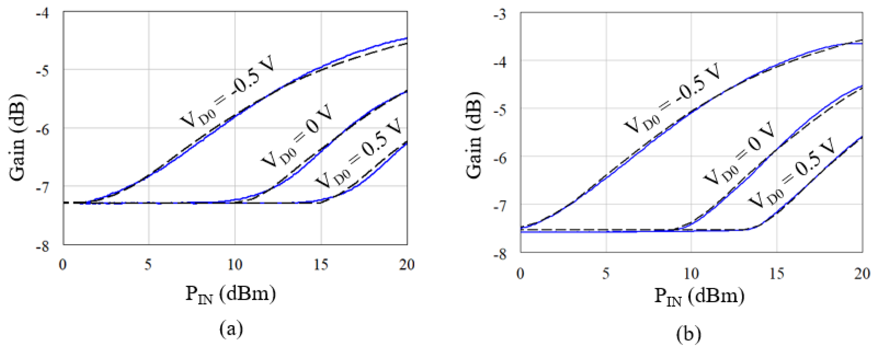
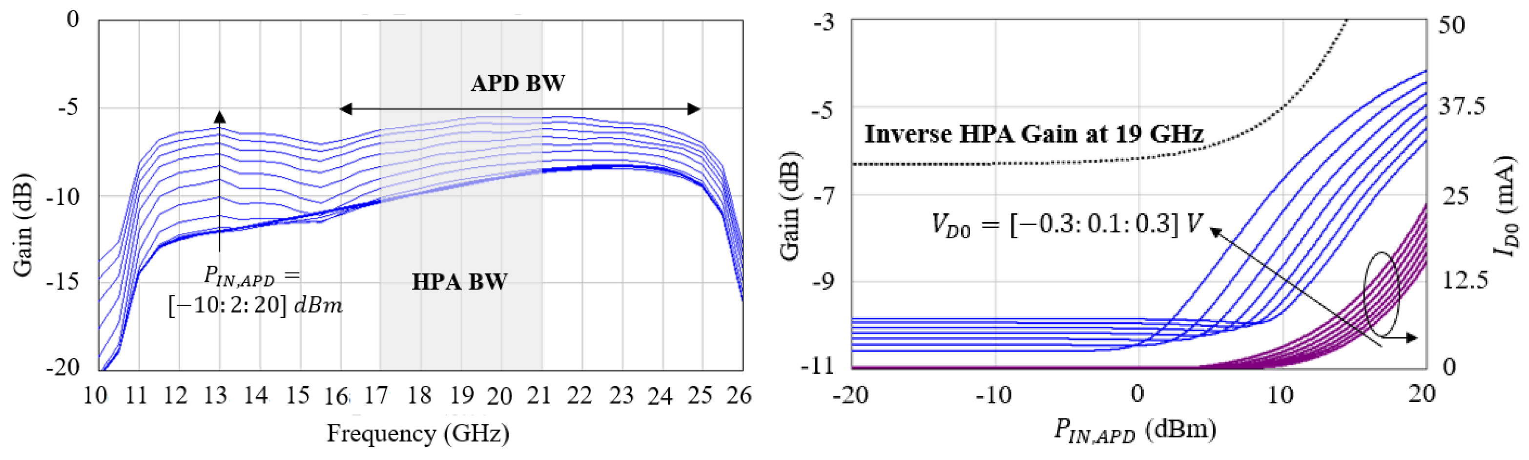
2.1. APD Amplitude Range

The theoretical gain characteristics of the proposed APD are shown in Figure 3a. Indicated on the diagram is the small-signal gain G S S , the large-signal gain G L S , and the maximum gain range Δ G M A X = G L S G S S . Please note that for high input powers, the diode generates harmonics that reduce the gain expansion at the fundamental (APD compression).
As anticipated previously, the phase difference Δ ϕ determines the APD gain range, and this is demonstrated analytically as follows. Let’s assume C T = 0 fF and Z S = 0 Ω , the nonlinear branch output voltage (8) reduces to
V O U T N L = V I N N L + Z 0 I S ( e α V D 1 )
The exponential can be approximated about V D 0 = 0 V with a Taylor series truncated at the first order,
e α V D 1 + α V D
Therefore, the nonlinear branch output voltage becomes
V O U T N L V I N N L + Z 0 I S α V D
As the diode voltage is V D = V I N N L V O U T N L , we have
V O U T N L V I N N L + Z 0 I S α ( V I N N L V O U T N L ) V I N N L
Therefore, the APD output voltage is
V O U T V I N 2 e j ϕ L I N + V I N 2 e j ϕ N L V I N 2 e j ϕ L I N + V I N 2 e j ( ϕ L I N Δ ϕ ) V I N 2 e j ϕ L I N ( 1 + e j Δ ϕ )
The APD voltage gain amplitude can be written as
| G V | = V O U T V I N 1 2 | 1 + e j Δ ϕ |
This last equation shows that the APD gain is only dependent on the phase difference Δ ϕ between the two branches.
For a more precise evaluation of the gain variation with Δ ϕ , the diode nonlinearity needs to be included by solving the APD model (12), and this results in Figure 4(Left). The small- and large-signal losses are minimized for Δ ϕ between 90 and 0 and their difference is due to the nonlinear phase shift introduced by the diode. The gain variation Δ G M A X , usually optimized for maximum APD+HPA improvement, presents a maximum of 4.8 dB for Δ ϕ = 84 ± k 360 . If the system requirements mandate minimizing APD large-signal losses instead of range, a choice of 6 is suggested for this diode.

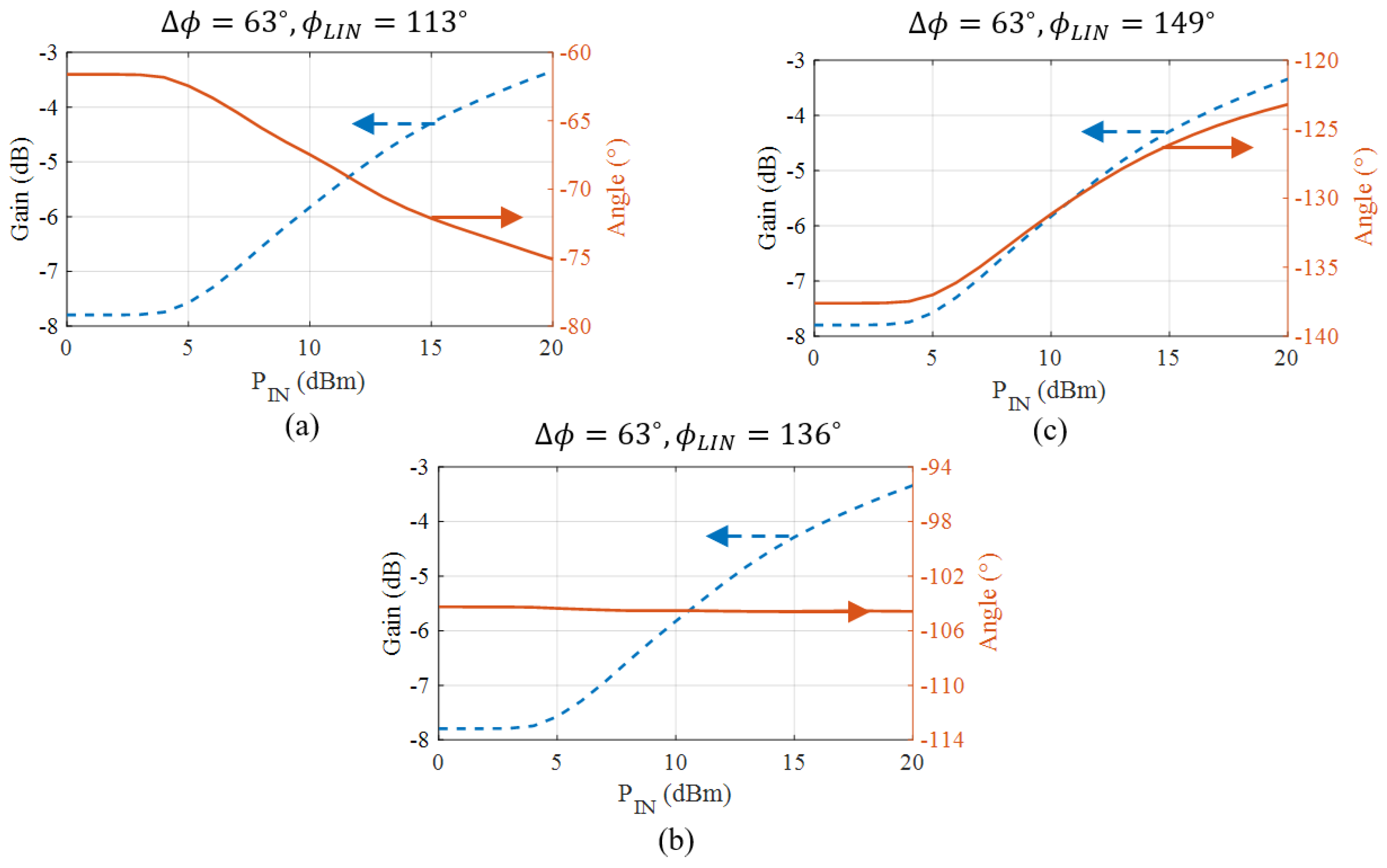
2.2. APD Phase Range

The theoretical phase characteristics of the proposed APD are shown in Figure 3b. Indicated on the diagram are the small-signal phase Φ S S , the large-signal phase Φ L S , and the maximum phase range Δ Φ M A X = Φ L S Φ S S . Please note that for high input powers, the diode generates harmonics that reduce the phase expansion at the fundamental (APD compression). The linear branch phase ϕ L I N can be used to control the APD phase range. This is demonstrated using (17) to calculate the phase
G V = V O U T V I N = ϕ L I N + ( 1 + e j Δ ϕ )
Given a fixed Δ ϕ that sets the amplitude range, this equation shows that ϕ L I N can be used to tune the APD phase variation.
The APD phase at small-signal, large-signal, and overall phase range are evaluated by solving the APD model (12). Figure 4(Right) shows that the phase variation reaches a maximum of 33 . 2 at ϕ L I N = 9 + k 180 . Periodic multiples of ϕ L I N will lead to a lower APD bandwidth, so we recommend keeping it at a minimum to interconnect the components. We also note that most HPAs require a phase rotation of ± 10 / 15 , e.g., [18], and so a different ϕ L I N may be chosen to match the APD to a specific HPA phase range.
It is interesting to note that depending on Δ ϕ and ϕ L I N choices, (19) shows that it is possible to generate a negative, neutral, or positive phase rotation depending on the sign of the two terms. This feature is demonstrated by solving the APD model and results in Figure 5 (constant amplitude shape in a dashed line). For all these characteristics, Δ ϕ = 63 and ϕ L I N is varied to achieve a negative, neutral, and positive phase variation, Figure 5a–c.

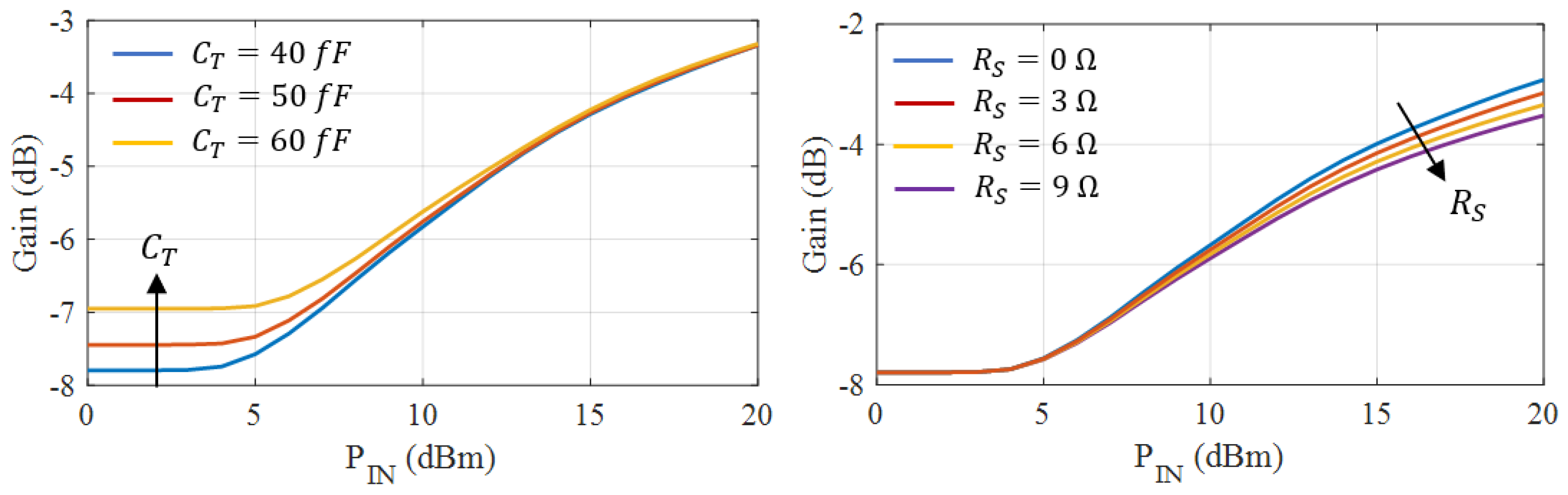
2.3. Impact of Diode Capacitance on APD Characteristics

The diode total capacitance C T has the effect of reducing the APD amplitude (and phase) range. This is demonstrated analytically by simplifying the APD model (12) as follows. In the small-signal region, the diode is off and I D = I S 0 . Therefore, the nonlinear branch output voltage reduces to
V O U T N L = Z 0 Z 0 + Z C T V I N N L
where Z C T = 1 / j ω C T . The APD output voltage becomes
V O U T = V I N 2 e j ϕ L I N + Z 0 Z 0 + Z C T V I N 2 e j ( ϕ L I N Δ ϕ )
Therefore, the APD voltage gain amplitude is
| G V | = V O U T V I N = 1 2 1 + Z 0 e j Δ ϕ Z 0 + 1 / j ω C T
This last equation captures the fact that for C T = 0 fF, | 1 / j ω C T | and | V O U T | = | V I N | / 2 or P O U T = P I N / 4 , and so the APD loses 6 dB. As C T increases, more power passes through the nonlinear branch, which reduces the APD amplitude (and phase) range. This is demonstrated in Figure 6(Left) by solving numerically the full APD model.

2.4. Impact of Diode Series Resistance on APD Characteristics

The diode series resistance R S has the effect of reducing the diode current as it introduces negative feedback in the exponent of the diode equation. This leads to a reduction in the APD gain (and phase) slope steepness. Assume a diode total capacitance C T = 0 fF and series inductance L S = 0 pH. The diode equation is simplified to
V O U T N L = Z 0 I S ( e α V D 1 ) V D = V D 0 + V I N N L V O U T N L 1 + R S Z 0
By calculating the derivative of V O U T N L with respect to R S , we can study the APD sensitivity to varying R S as follows:
d V O U T N L d R S = I S e α V D α V O U T N L
Noting that the first equation of (23) can be recursively substituted here, we have
d V O U T N L d R S = α ( V O U T N L + Z 0 I S ) V O U T N L Z 0 = α I S V O U T N L α Z 0 V O U T N L 2
As I S is generally in the nA–pA range, the linear term can be neglected. Thus, the nonlinear branch sensitivity to R S is
d V O U T N L d R S α Z 0 V O U T N L 2
Given this negative sign, increasing R S has the effect of reducing the APD amplitude (and phase) slope steepness, especially at higher voltages, given the quadratic dependence. Figure 6(Right) demonstrates numerically this conclusion by solving the APD model.

2.5. Impact of Diode Ideality Factor on APD Characteristics

The diode ideality factor n has the effect of shifting the APD turn-on “knee”. This is demonstrated analytically by simplifying (12) as follows. Assume Z S = 0 Ω and C T = 0 fF, the sensitivity of the nonlinear output voltage to n is the derivative with respect to n of the first equation in (23), namely
d V O U T N L d n = Z 0 I S e α V D q V D n 2 k T
Noting that the first equation in (23) can be recursively substituted here, we have
d V O U T N L d n = ( V O U T N L + Z 0 I S ) q V D n 2 k T
As I S is generally in the nA or pA range, the term Z 0 I S is neglected. Assuming a lossless diode ( V D = V D 0 ), we have
d V O U T N L d n V O U T N L q V D 0 n 2 k T
This equation shows that increasing ideality factors n has the effect of “reducing” the APD amplitude characteristic. This concept is also visible in Figure 7, which is obtained by solving numerically the APD model for n = [ 1 , 1.2 , 1.4 , 1.6 ] .
We note that a similar derivation to (29) can be performed for the temperature T. Temperature drifts have the same effect of changing the ideality factor n.
Equation (29) also suggests the possibility of tuning the diode bias V D 0 to compensate for temperature effects or to change the turn-on “knee” of the diode.

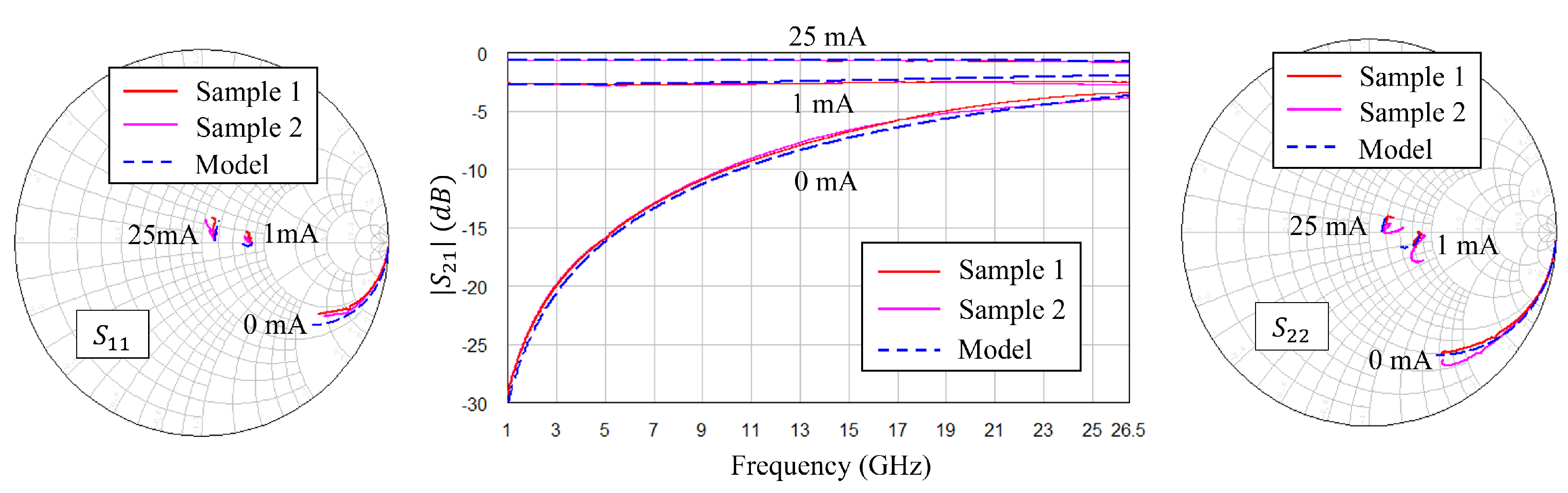
2.6. Model Validation

In this section, the large-signal measurements of Section 4 are used to validate the APD model (12). Figure 8 shows measured vs. modeled APD gain at 15 and 21 GHz and for the biases V D 0 = [ 0.5 , 0 , 0.5 ] V. For this comparison, the diode capacitance and resistance have been slightly varied from the nominal values ( C T = 40 fF and R S = 6 Ω ) to C T = 58 fF and R S = 10 Ω , while n and I S are the same.
An increased diode capacitance can be due to the lack in the APD model of the diode junction capacitance (10 fF at V J = 0 V) and because of the added coupling in the APD board. As for the resistance, the diode manufacturer provides a resistance range of 7–9 Ω in the datasheet [19], thus justifying a slight increase in R S . The additional resistance can be due to the diode pads.
Also, the diode biases have been slightly adjusted ( ± 0.2 V) to match the measurement results, and this is possibly due to mismatches introduced by a real Wilkinson splitter that is not considered in the model. These mismatches will, in fact, reduce the diode drive, and therefore, the modeled diode threshold does not correspond to the measured one. Given these adjustments, the APD model predicts the measured APD characteristics well at the two frequency edges (15 and 21 GHz) and for varying diode biases, as shown in Figure 8.

2.7. Diode Selection

The APD model can be used to quickly evaluate different diodes before proceeding with the circuit design. Given the K-band operating frequency of the HPA, GaAs Schottky diodes are preferred to other technologies for their lower parasitic. After a component search, two commercial GaAs Schottky diodes have been identified, and their parameters are reported in Table 1. Both diodes achieve a 7 V breakdown voltage (BV) and a high cut-off frequency f C of several hundred GHz. The difference between these diodes is that Diode 1 has a lower n ( n = 1 is an ideal diode), a higher series resistance R S , and a lower capacitance C T .
Figure 9 shows the APD model gain and phase response for the two diodes. Diode 1 has a wider amplitude expansion (1 dB more than Diode 2) and a wider phase variation ( 7 more than Diode 2), mainly because of its lower total capacitance C T , as discussed in Section 2.3. The lower R S of Diode 2 provides a small improvement in the amplitude steepness at higher input powers that is insufficient to compensate for the higher C T .
On the same plot, the inverted characteristics of the HPA are reported. At 19 GHz, the HPA was measured up to 6 dB and 17° into compression. As can be seen, the APD realized with Diode 1 can fit on a wider range of the HPA gain and phase response, thus suggesting higher HPA linearity, output power, and efficiency improvements with this diode.

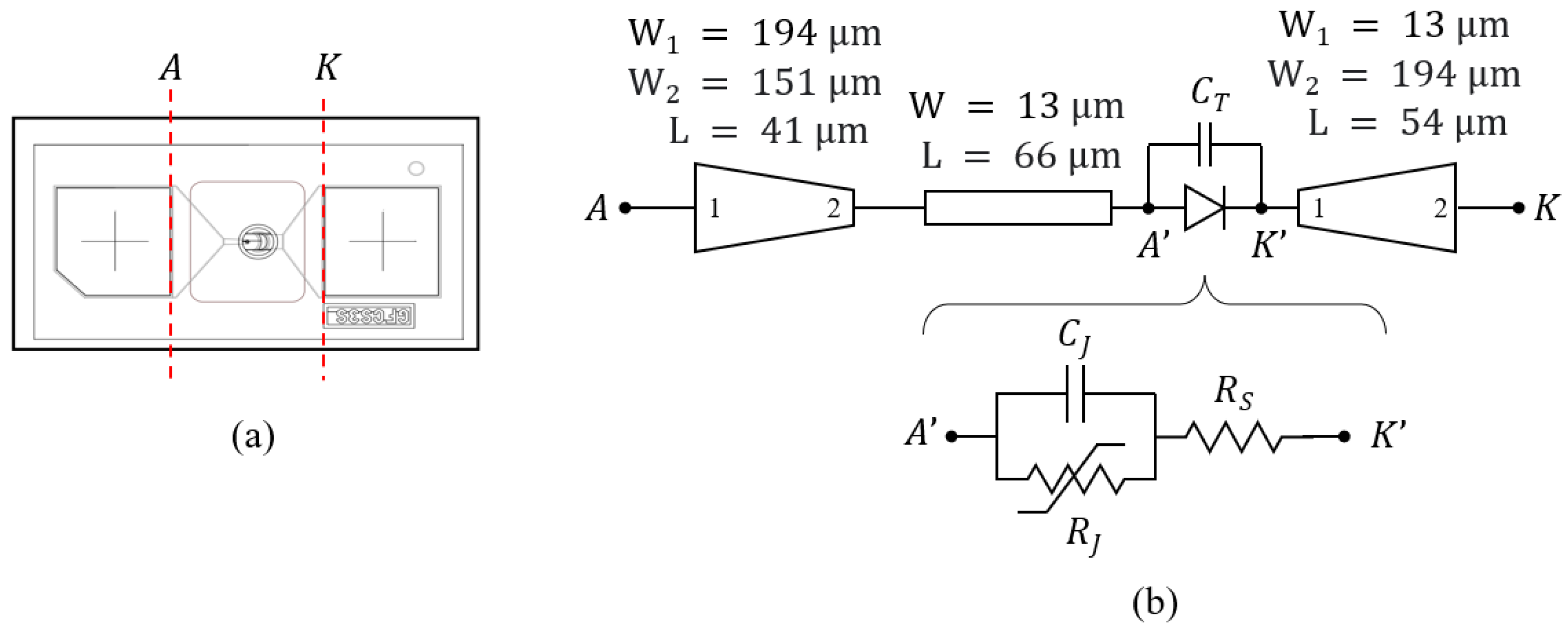
3. Diode Modeling for APD Design

This section discusses the modeling, extraction procedure, and validation of the APD diode nonlinearity. An accurate model for nonlinearity plays an important role in the design of the APD circuit; however, few models capable of operation at high frequencies are available, especially for high-performance GaAs Schottky diodes.
Some academic research in this direction has been recently conducted by [20] for Diode 2, which, however, resulted in lower performance in our comparison. In [20], the procedure was validated up to 18 GHz, and it employs bond-wiring of the diode to the access lines, which is not suitable for this application given the bond-wire inductance that would reduce the APD amplitude and phase range.

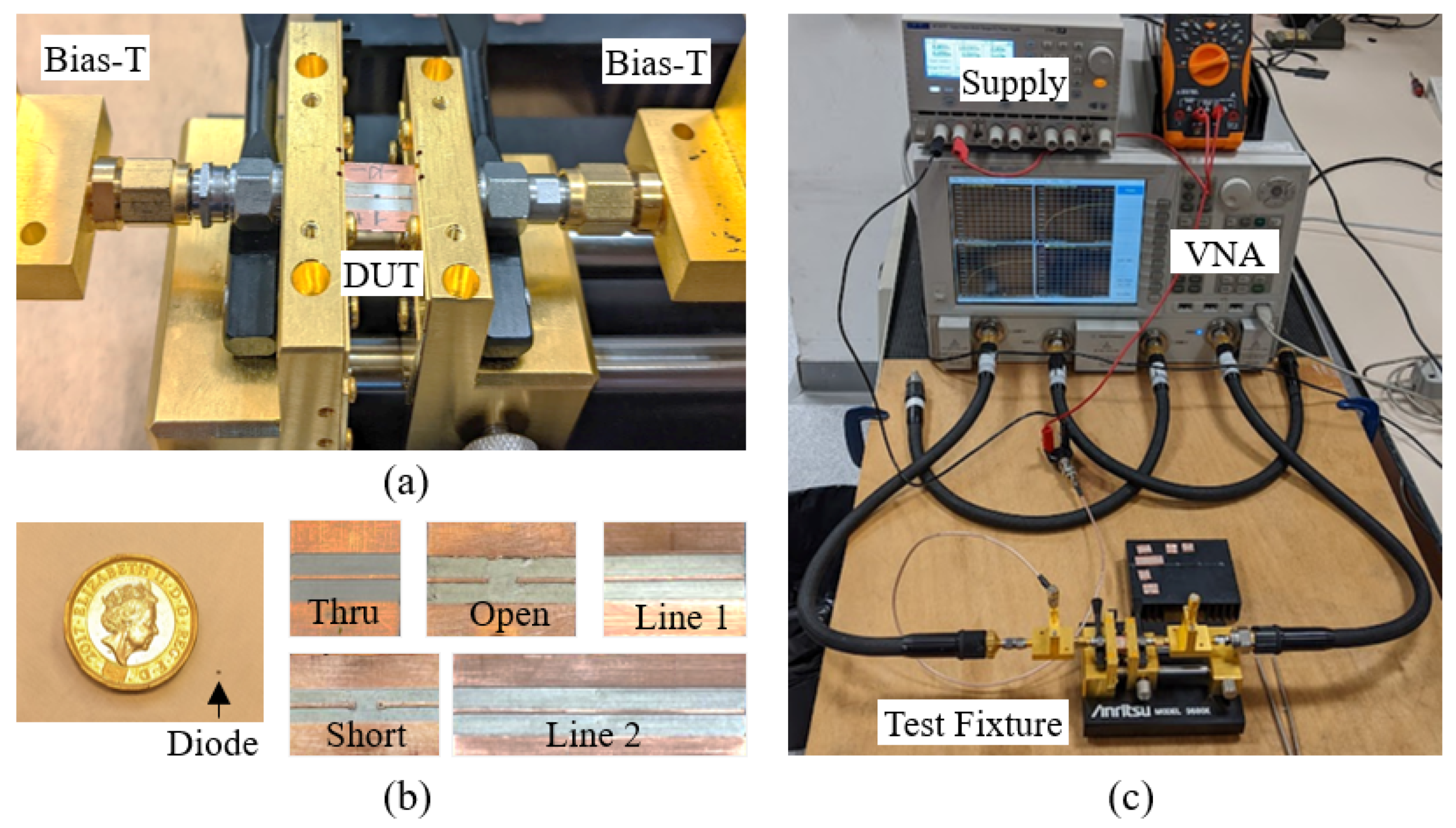
3.1. Diode Characterization

The diode is characterized by the same substrate used for fabricating the APD circuit. A Rogers 3003 substrate with a relative dielectric constant ϵ r = 3 , a height of 127 μ m, and a copper thickness of 17 μ m is used. With this substrate, the 50 Ω line width is 303 μ m, which is well matched with the diode width of 330 μ m. For the characterization, the diode is mounted in a series configuration with 5 mm access lines on each side. A series configuration is preferred to the shunt configuration to avoid performance deterioration due to the via-hole inductance.
An Anritsu 3680K test fixture is utilized to provide 2.92 mm connectors to the diode fixture, as shown in Figure 10a. The diode bias is applied with two bias-Ts (HP 11612A, Keysight Technologies, Santa Rosa, CA, USA). The anode bias-T provides a positive or negative bias, while the cathode bias-T provides a ground connection. These bias-Ts are connected to a 26.5 GHz PNA-X (Keysight N5242A, Keysight Technologies, Santa Rosa, CA, USA).
A Thru-Reflect-Line (TRL) calibration kit based on the Rogers 3003 substrate is realized as shown in Figure 10b. For this kit, the frequency range is 1 to 26.5 GHz (upper-frequency limit of the VNA) and results in the requirements of two 90° lines. The first line is 15.8 mm long and is 90° at 3.07 GHz and covers the frequency range from 1 GHz (29.7°) and 5.15 GHz (152°). The second line is 3.1 mm long and is 90° at 15.8 GHz and covers the frequency range from 5.15 GHz (29.5°) to 26.5 GHz (152°). These lines, therefore, are within the 0–180° limit. A TRL de-embedding algorithm is then used to calibrate the A-K diode reference planes and remove the effects of the diode pads. Figure 10c shows the test setup used for this characterization.

3.2. Diode Modeling

For simplicity’s sake, the diode description used for the APD model does not account for the nonlinear junction capacitance, as this is typically smaller than the total capacitance C T (10 fF vs. 40 fF). For the APD design, the diode junction capacitance C J is described by
C J = C J 0 1 V D V J M
The zero-bias junction capacitance is C J 0 = 10 fF, and the junction grading coefficient is M = 0.25 . With these parameters, a Spice diode model is created in AWR.
Figure 11 shows the measured vs. simulated I/V characteristic at room temperature and in static bias conditions. Good agreement is found between the two samples and the model. At higher dissipations, a slight deviation in the current can be caused by self-heating, given the high thermal resistance of the diode 0201 die. For these measurements, the cable and bias-T resistances ( 2 × 0.5 Ω for the two HP 11612A bias-Ts) have been de-embedded.
The diode access lines are also included in the model. As the diode is fabricated on a GaAs substrate of dielectric constant ϵ r = 12.9 , thickness of 203 μ m, and tan δ = 0.00056 , the diode access lines are modeled in MWO with MTAPER and MLIN elements with geometries indicated in Figure 12.
The measured vs. simulated S-parameters are shown in Figure 13 for three biases and two samples. To aid the match between simulations and measurements, a shunt capacitor at pins A and K is placed to simulate the substrate coupling with the diode. We note that this coupling will also be present in the APD circuit as it employs the same diode and substrate. As can be seen in the S-parameter plots, a good agreement is found between the model and measurements from 1 to 26.5 GHz.

4. Linearizer Design and Characterization

Using the diode model of Section 3, the APD circuit is designed in AWR. The nonlinear branch uses the Schottky diode mounted in a series configuration and connected to a line of 303 μ m width. The diode bias is provided by two λ / 4 lines of 200 μ m width and 3.64 mm length. The DC bias is removed by two 0201 DC block capacitors of 22 pF (Knowles CSB-140-20x10x4-5-G-220-M) with 50 GHz self-resonance frequency.
The transmission line in the linear branch is 10.3 mm long or ϕ L I N = 363 at 19 GHz, while the line in the nonlinear branch is 8.4 mm long or ϕ N L = 283 at 19 GHz. Therefore, a phase difference of Δ ϕ = 80 at 19 GHz is introduced. The two branches are connected to a Wilkinson splitter and combiner, with the 100 Ω isolation resistor realized with a 0402 resistor with high self-resonance frequency. The circuit layout is electro-magnetically simulated with AWR Axiem. The diode DC bypass capacitors and bias lines have been optimized to provide a good baseband termination in the video bandwidth of the APD circuit. The layout of the circuit is shown in Figure 14.
The APD gain is simulated over a large frequency range (10–26 GHz) and for various input powers between −10 and 20 dBm at steps of 2 dB, Figure 15(Left). The designed APD circuit exhibits a large-signal bandwidth between 16 and 25 GHz (9 GHz), corresponding to a fractional bandwidth of 44 %. At the lower end, this bandwidth is limited by the bias line resonance. Going towards higher frequencies, the gain expansion is reduced by the diode total capacitance C T , as discussed in Section 2.
The APD gain amplitude and phase tuning range at 19 GHz are evaluated for diode bias voltages between −0.3 and 0.3 V at steps of 0.1 V, and the results of these simulations are reported in Figure 15(Right). The diode bias voltage changes the APD small-signal response because of the dependency of C J ( V D ) as in (30). This variation can be easily compensated for by the APD post-amplifier. When the diode bias increases, the APD “knee” amplitude and phase move towards higher powers.
Finally, the APD diode voltage is simulated in Figure 16 at the upper-frequency edge of the HPA bandwidth ( f 0 = 21 GHz) to verify that the diode voltage does not exceed the 7 V breakdown of Diode 1 [19]. Please note that peak voltages are within 75% voltage derating typically used for space applications [21].

4.1. Simulated APD with Measured HPA-in-the-Loop

Before proceeding with the fabrication of the APD circuit, the simulated APD linearizer is evaluated with the actual HPA at 19 GHz using the following procedure:
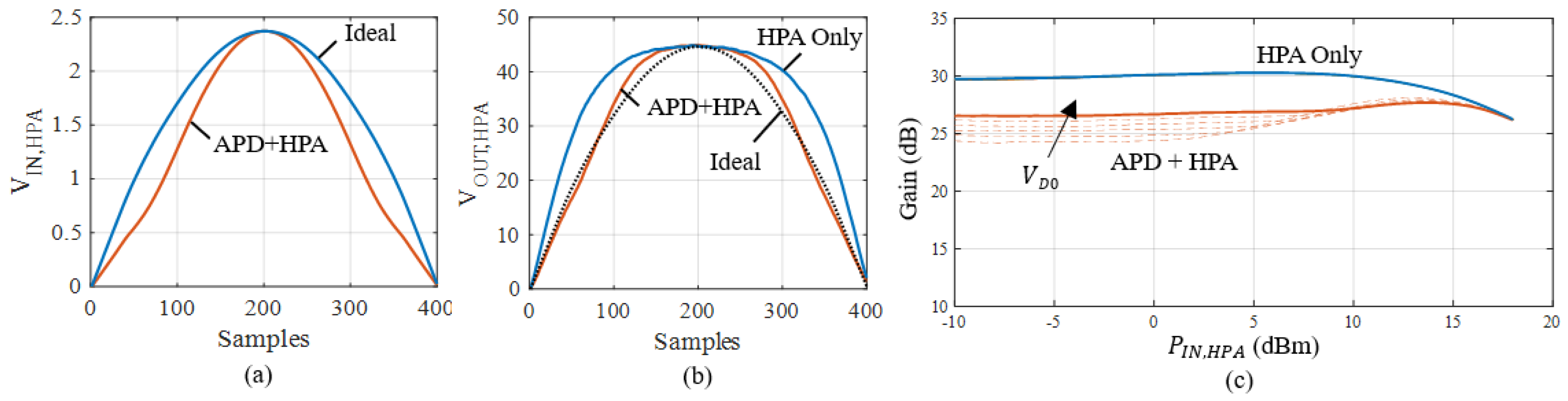
  • A simulation with an amplitude-modulated sine wave at the APD input is performed to generate the pre-distorted signal, Figure 17a. This simulation is a time-domain harmonic balance (APLAC Transient in MWO);
  • The pre-distorted signal is transferred to the measurement setup and is then applied to the HPA input. An optimal diode bias of V D 0 = 0.67 V is found by iterating between (1) and (2). For V D = 0.67 V, the APD+HPA output amplitude approximates the ideal sine wave amplitude, Figure 17b.
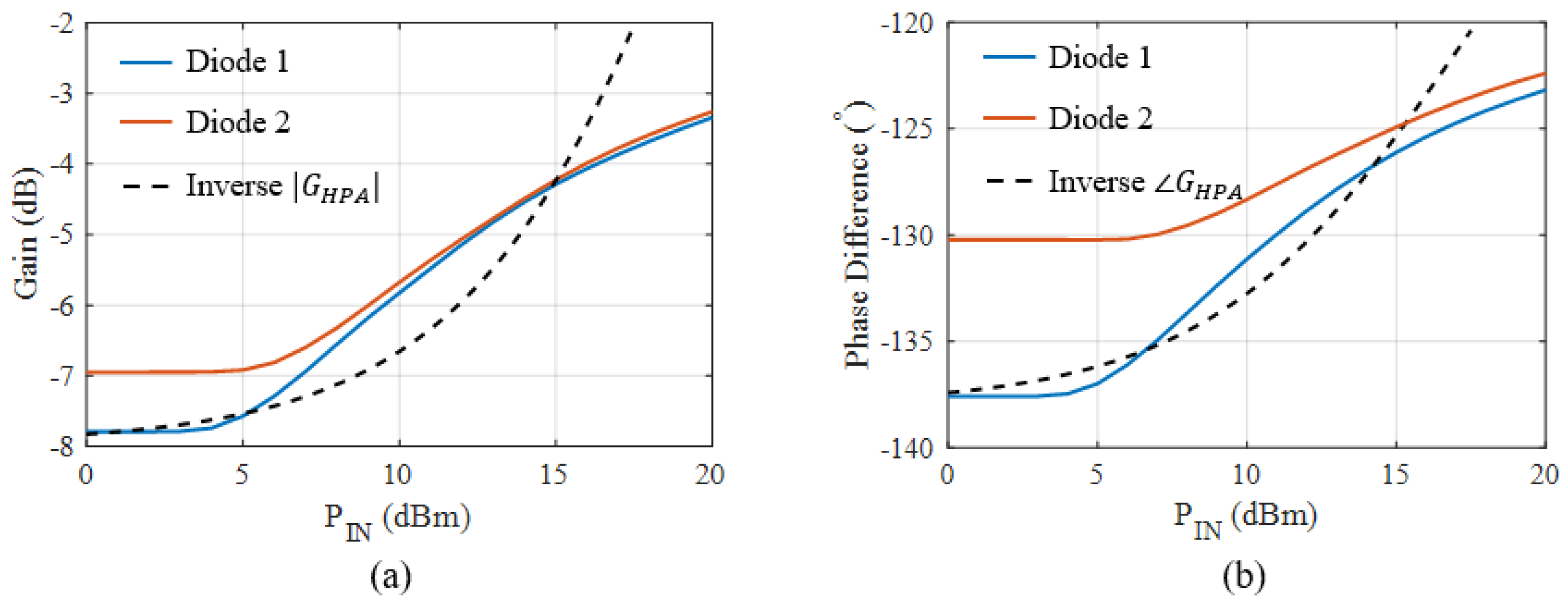
  • The HPA gain with and without simulated APD is computed and reported in Figure 17c. As can be seen, the small-signal gain with APD at 19 GHz is reduced by approximately 4 dB, while at a large-signal, APD reduces the HPA gain compression (hence less distortion) for the same maximum output power.

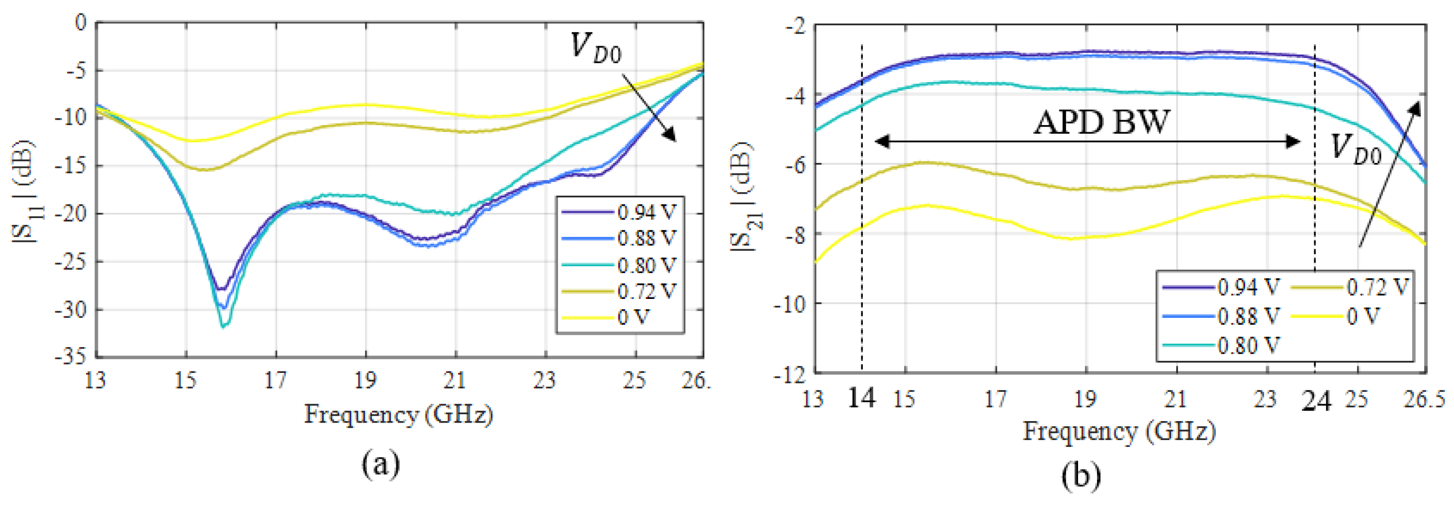
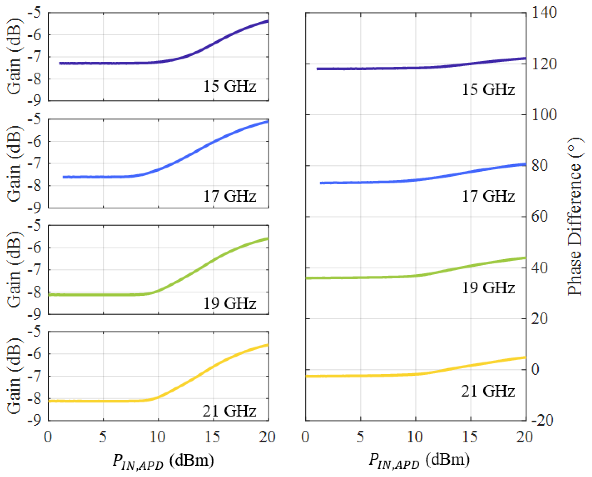
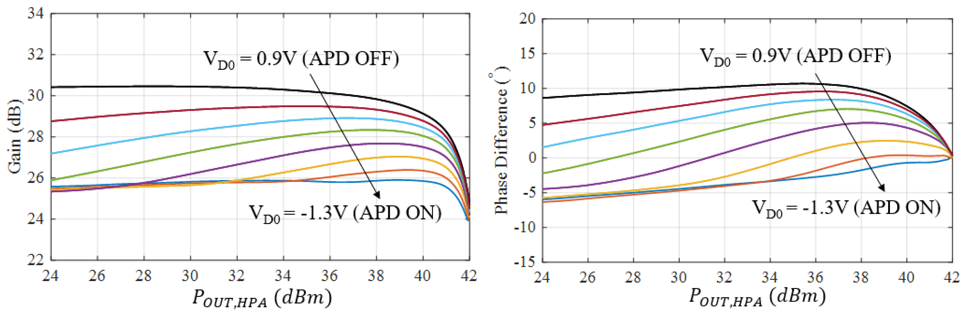
4.2. Small- and Large-Signal APD Characterization

Using the Keysight PNA-X vector network analyzer N5242A of Figure 10c, the S-parameters of the APD circuits were first measured for different diode biases, and result in Figure 18. A positive diode bias was used to simulate the diode turn-on that is caused by the RF input power, and so verify the correct APD operation. As shown by Figure 18, the APD input | S 11 | improves from about −7 to −15 dB as the diode is turned on. Thanks to the input Wilkinson divider, an acceptable input match is maintained even when the diode is off, thus avoiding the need to introduce bulky and bandwidth-limiting isolators.
As for the APD gain, the | S 21 | reduces for positive diode biases, thus providing an expanding gain characteristic. This measurement also confirms the simulation results shown in Figure 15 with good approximation, especially when the diode is fully on. From these small-signal measurements, a usable −1 dB bandwidth for this linearizer of 14–24 GHz is observed. As for the APD phase, the S 21 reduces for increasing input biases, as shown in the zoomed box of Figure 18.
A large-signal setup based on the Keysight PNA-X and booster/driver amplifier (Keysight/HP 83020A) is used to characterize the APD with input powers up to 20 dBm. A bi-directional coupler is placed after the driver to sense the incident and reflected voltage waves at the APD input, and a 30 dB attenuator is used at the APD output to prevent accidental overdrive of the PNA-X receivers. Power calibration is performed at the APD reference planes across the bandwidth. Figure 19 shows the APD characteristics for V D 0 = 0 V. These measurements confirm the simulated large-signal bandwidth of 6 GHz. The same large-signal setup is used to measure the APD characteristics at different biases and frequencies of Figure 8, which are used for APD model validation discussed in Section 2.6.

5. APD-HPA Performance Evaluation

The APD circuit is specifically designed to correct the amplitude and phase variation (see Figure 9) of a 3-stage HPA from UMS (CHA8252-99F [3]). This HPA is realized with the UMS 0.15 μ m GaN-on-SiC process and can provide ∼10 W output power with more than 35% PAE in the 17–21 GHz band. The three stages of this class-AB HPA are biased at 18 V and 308 mA and provide a small signal gain between 28.5 and 31.5 dB across the band. The HPA efficiency, however, rapidly decreases when the HPA is backed off. For example, at 10 dB backoff, the PAE at 19 GHz is only 10–12% [3]. The HPA MMIC is mounted on a test fixture providing 2.92 mm connectors and DC bypassing (up to 1 μ F).

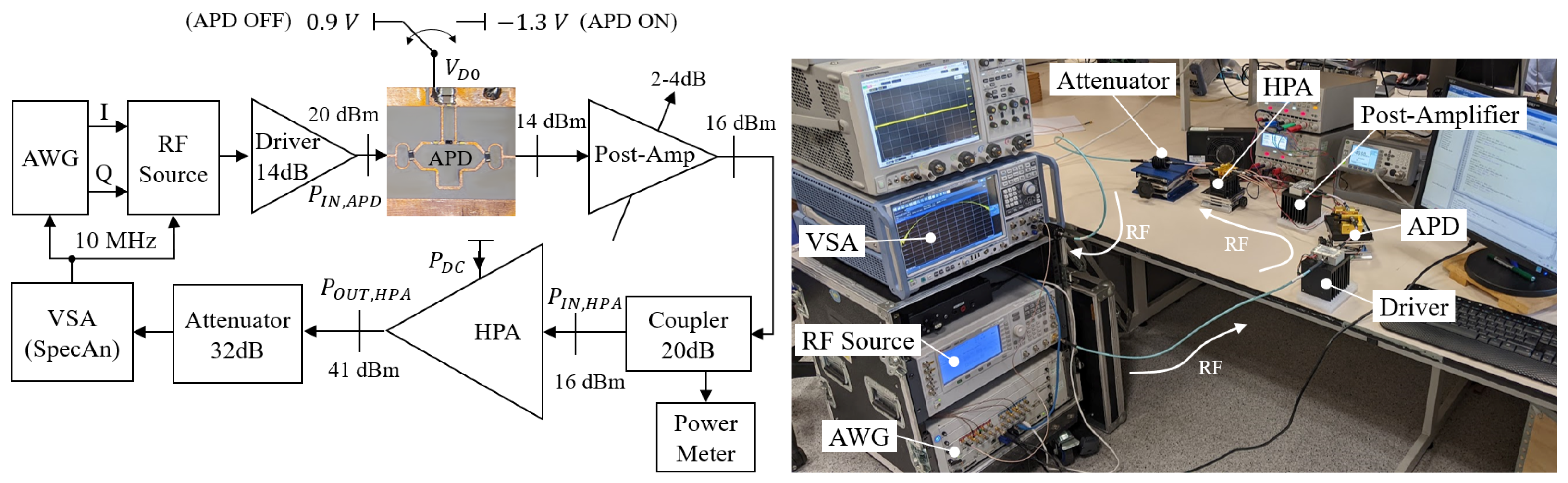
5.1. Wideband Measurement Setup

The measurement setup of Figure 20 is built to measure the HPA with and without APD. An arbitrary waveform generator (AWG, Keysight M8190A) generates two analog I/Q differential signals that modulate the input of a wideband RF source (Keysight E8267D) capable of 1.2 GHz instantaneous bandwidth. The RF source output signal is amplified by a 13–26.5 GHz driver amplifier (Mini-Circuits ZVM-273HP+) up to 20 dBm necessary to excite the APD nonlinearity.
Depending on the carrier frequency, the APD attenuates by 5–6 dB when the APD input power is 20 dBm, Figure 19. To recover this loss, a post-amplifier (variable attenuator + Mini-Circuits ZVM-273HP+) is introduced to restore the HPA drive of 16 dBm. This power is sensed by a power meter connected to a coupler at the HPA input. The signal is then amplified by the HPA up to 41 dBm. A 32 dB attenuator is connected between the HPA and a vector signal analyzer (VSA, Rohde & Schwartz FSW43, Munich, Germany) with 1.2 GHz bandwidth.
Scalar calibration of the setup is performed between 17 and 21 GHz. First, the setup input gain is measured by turning off the APD ( V D 0 = 0.9 V) and by measuring the power difference between the HPA input and RF source output. The calibration factors at f 0 = [ 17.5 , 19.0 , 20.5 ] GHz are Δ G I N ( f ) = [ 0.2 , 0.0 , 0.9 ] dB. Subsequently, the setup output attenuation is measured by replacing the HPA with a 2.92 mm “thru” connector and then by measuring the power difference between the HPA output and the VSA input. The calibration factors at f 0 = [ 17.5 , 19.0 , 20.5 ] GHz are Δ A O U T = [ 0.3 , 0 , 0.2 ] dB. For both input and output calibration factors, the gain and attenuation at 19 GHz (central value) have been set as a reference, hence the 0 dB correction. To achieve precise NPR measurements, the DC offset was calibrated by changing the RF source I/Q offset voltages to cancel out the leaking tone.

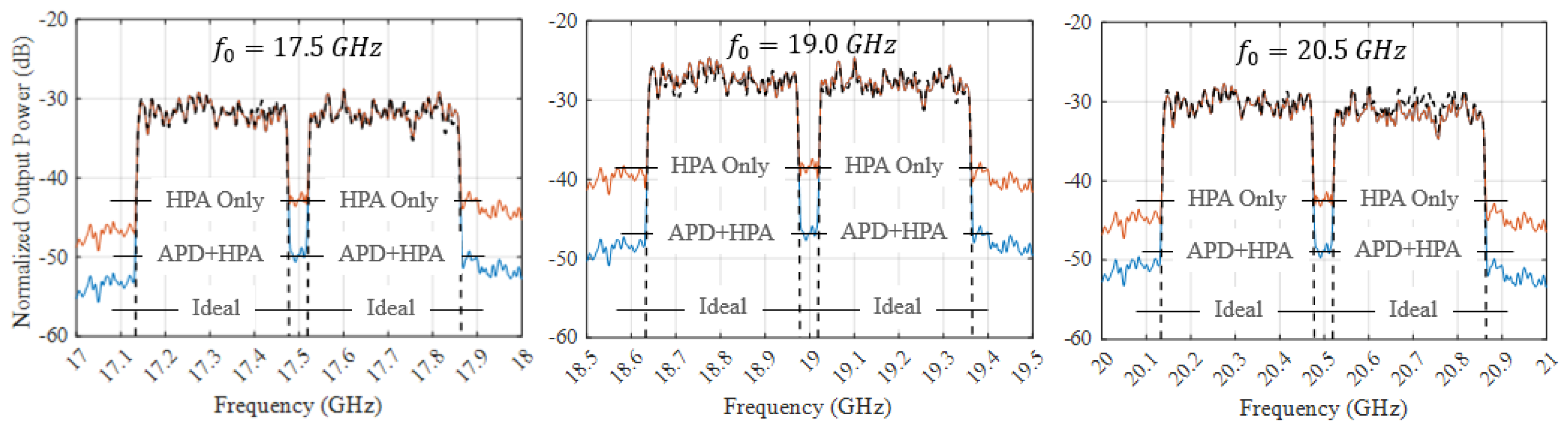
5.2. Performance with APD

The next step is finding the diode bias voltages that ensure maximum gain and phase flatness. This is achieved by sweeping the diode biases with a narrowband Gaussian pulse [22] at 19 GHz, as shown in Figure 21. As the diode bias becomes more negative, the APD+HPA combined response starts to flatten in the backoff region and then reaches the compression where APD expansion and HPA compression cancel out, thus realizing an extended linear power range. As shown in Figure 21, for V D 0 = 1.3 V the APD+HPA presents less than 2 dB compression for the same output power whereas when the APD is not used, the compression is over 6 dB. Similar results can be found for the phase where the APD reduces the variation by 5° ( 11 without APD and + 6 with APD). This tuning has also been performed for each of the three considered frequencies and results in V D 0 = [ 1.4 , 1.3 , 1.4 ] V for f 0 = [ 17.5 , 19.0 , 20.5 ] GHz.
A noise-like wideband signal is generated using the multi-signal algorithm of [23]. The algorithm has been configured to generate a signal with B = 750 MHz bandwidth, a B N = 50 MHz notch bandwidth in the middle for NPR measurements, and a PAPR of 12 dB. In this way, it is possible to simulate a noise-like signal of 140 carriers as needed by the application (DOCSIS 3.0 channel of 5 MHz bandwidth, spaced 5 MHz apart). With this spectrum, the noise–power ratio (NPR) is measured using the following definition:
NPR ( dB ) = 10 log B N P O U T , H P A ( f ) d f B P O U T , H P A ( f ) d f
The NPR has been evaluated without and with APD to evaluate the APD benefit, and results are shown in Figure 22. For these measurements, the diode bias has been adjusted to the optimal values of V D 0 = [ 1.4 , 1.3 , 1.4 ] V at f 0 = [ 17.5 , 19.0 , 20.5 ] GHz. As APD linearization operates by reducing the backoff gain, the signal average output power changes when APD is introduced. To provide a fair comparison between the HPA-only case (APD disabled) and the APD+HPA case (APD enabled), the average output power has been adjusted to be the same as the HPA-only case. For these measurements, the NPR improves by [ 7.2 , 8.2 , 6.5 ] dB for the same 750 MHz signal at f 0 = [ 17.5 , 19.0 , 20.5 ] GHz. As for the ACPR, given the large bandwidth of the considered signal (750 MHz) and the setup bandwidth of 1.2 GHz, it was not possible to fully capture the sides of the spectrum. This is also not necessary as the application (cable modem with DOCSIS signal) does not pose ACPR requirements.
Next, the signal average has been swept to compare the case without and with APD over the bandwidth, Figure 23. In this plot, a scale has been added on the top x-axis, reporting the measured average HPA efficiency for each average output power. For NPRs around 30 dB, the APD benefit is limited by the noise floor. For NPRs below 15 dB, the APD is limited by the HPA compression. For NPRs between 30 and 15 dB, APD allows for improved HPA output power and efficiency over the whole frequency range. Improvements are the highest for NPR > 30 dB, and they decrease for higher output powers as the APD is not able to recover the HPA hard compression.

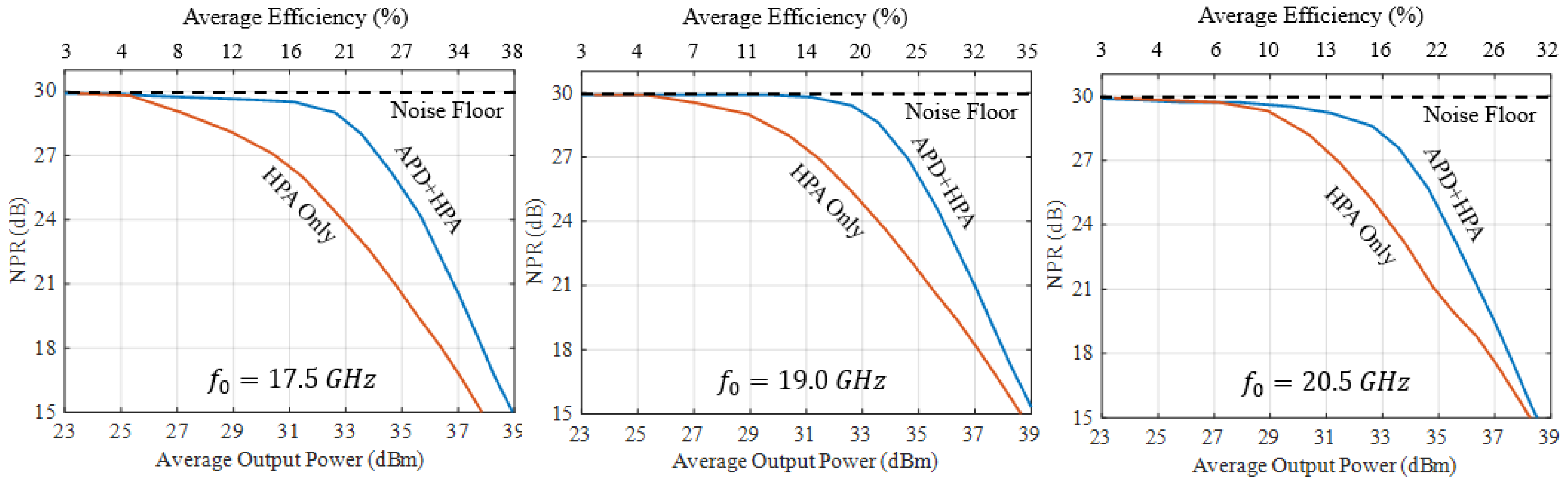
5.3. Estimated APD+HPA Efficiency Including Post-Amplifier

In this section, the power consumption due to APD is estimated with the data available on commercial amplifiers compatible with the 17–21 GHz frequency range and power level to drive the HPA (approximately 17 dBm). At these powers and frequencies, GaAs MMICs are commonly used; for example [24,25,26] present DC power consumptions between 0.7–1 W, and achieve a gain of 23 dB, thus requiring insertion of an attenuator as the APD loss is only 5–6 dB. For 5–6 dB gain at K-band, a single-stage GaAs amplifier should suffice and result in a lower power consumption.
The overall efficiency improvement obtained with APD can be quantified using the following formula:
η D = P O U T , H P A P D C , H P A + P D C , P o s t A m p
As the DC power consumed by the APD block is practically zero (there is a small rectified current by the diode, which is, however, less than a few mA on average), the main power consumption caused by APD is due to the post-amplifier, P D C , P o s t A m p . Assuming a driver stage of [25] which achieves 21 dBm output power (OIP3 of 33 dBm) and draws 0.7 W, Table 2 reports the estimated efficiency, including the driver stage. For NPRs of 28, 24, and 20 dB, the introduction of the post-amplifier reduces the APD+HPA efficiency by only about 1–2%, thus suggesting the viability of APD for overall efficiency and power increase for this HPA.

5.4. Comparison with State-of-the-Art

Table 3 compares the performance achieved by the presented APD linearizer with other relevant APD works. Comparing different APD architectures is a difficult task, given the multitude of architectures, technologies, and frequencies. Therefore, we identified the fractional bandwidth, small-signal loss, large-signal gain, and phase expansions as the most suitable metrics for this comparison.
In the first group of the table, single-branch linearizers are compared [6,9,10,27,28]. Single-branch linearizers present a fractional bandwidth of 3–7% and introduce significant small-signal losses of 12–20 dB, possibly because of the high isolation achieved when the nonlinearity generator is off. However, the large-signal gain and phase expansion is significant and can be up to 8 dB/28° [10]. Such a wide gain expansion is, however, not necessary in practice, as most HPAs will clip after 4–5 dB of compression.
Table 3. Comparison with state-of-the-art APD Linearizers.
Ref.Archi.Nonlinearity Generator 0 (GHz)BW
(GHz)
Fractional BW (%)Small-Signal Gain | G SS | (dB)Gain Expansion | Δ G MAX | (dB)Phase Expansion | Δ Φ MAX | (°)
[6]Single Branch APDTwo Shunt Schottky Diodes20.15%12525
[9]Single Shunt Diodes140.755%-430
[10]Two Shunt Schottky Diodes6023%16 *828
[25]Shunt Diodes60.47%17620
[26]Schottky + Varactor Diodes5--20 *430
[11]Dual Branch APDPIN Diodes3027%20 *523
[13]Schottky Diode (MMIC)29414%14 *8 *40 *
[14]Shunt Schottky Diode20210%27 *4 *9 *
[28]GaN Amplifier0.80.225%-2 *10 *
[29]GaAs Amp. + Diode (MMIC)2628%10440
[12]Schottky Diode19316%-1350
This GaAs Schottky Diode18633%838
* Value extracted from a plot.
Dual-branch linearizers provide comparable small- and large-signal losses to the single-branch APDs but present wider fractional bandwidths of 7–25%. Such wider bandwidth is due to a less stringent trade-off between nonlinearity isolation and small-signal losses [12,13,15,29,30]. However, the bandwidth of all these linearizers does not exceed 4 GHz.
Our work provides less nonlinear gain and phase expansion than others but achieves significantly wider fractional bandwidths. Achieving higher gain and phase expansions is most of the time unnecessary as typical HPAs are used 3–4 dB into compression and exhibit ± 10 20 phase variation (as also the HPA considered here). As it can also be seen in the NPR measurements vs. HPA efficiency/output power of Figure 23, most of the APD benefit is achieved between 5 and 15 dB in backoff from the P 1 d B and therefore very high nonlinear gain expansion is most of the time unnecessary. Additionally, the proposed APD provides a significantly lower loss of only 5–6 dB over the whole APD bandwidth, thus requiring less post-amplifier gain or gain stages for lower cost, less power consumption, and easier system integration.

6. Conclusions

This paper presents the theory, design, and application of a dual-branch series-diode analog pre-distortion (APD) linearizer. A new frequency-dependent large-signal APD model is presented and used to study the APD behavior for different phase lengths between the linear and nonlinear branches. This model is used to investigate the impact of different diode parameters on the APD gain and phase characteristics. The APD model is then used to compare different diode models with reference to the inverted HPA gain and phase trajectory. The selected diode is characterized, modeled from 1 to 26.5 GHz, and used for the design APD circuit. After an extensive simulation workflow, a co-simulation of the APD with the measured HPA suggests a gain compression reduction by 4 dB at 19 GHz. Characterization of the fabricated APD reveals a bandwidth of 6 GHz (15–21 GHz) with a gain expansion of 3 dB and a phase rotation of 6°. This APD improves the HPA efficiency by ∼5–9% while boosting output power by ∼1–2 W at 19 GHz for this 10 W/35% HPA. This efficiency improvement decreases by only 1–2% when accounting for the power consumption of the APD post-amplifier, thus suggesting overall efficiency and power improvements with APD at K-band frequencies.

Author Contributions

Conceptualization, T.C., A.T. and K.M.; Methodology, T.C., P.K. and T.W.; Software, T.C.; Validation, T.C.; Formal analysis, T.C.; Investigation, T.C., S.O., A.T., P.K. and K.M.; Resources, T.C., S.O., A.T., P.K. and T.W.; Data curation, T.C.; Writing—original draft, T.C., S.O. and T.W.; Writing—review & editing, T.C., S.O. and K.M.; Visualization, T.C.; Supervision, T.C. and A.T.; Project administration, T.C. and T.W.; Funding acquisition, T.C. and K.M. All authors have read and agreed to the published version of the manuscript.

Funding

This research received no external funding.

Data Availability Statement

Data are contained within the article.

Conflicts of Interest

Authors Andy Tucker, Peter Krier are Tudor Williams are employed by the company Filtronic PLC. The remaining authors declare that the research was conducted in the absence of any commercial or financial relationships that could be construed as a potential conflict of interest.

References

  1. Katz, A.; Gray, R.; Dorval, R. Truly wideband linearization. IEEE Microw. Mag. 2009, 10, 20–27. [Google Scholar] [CrossRef]
  2. Katz, A.; Wood, J.; Chokola, D. The evolution of pa linearization: From classic feedforward and feedback through analog and digital predistortion. IEEE Microw. Mag. 2016, 17, 32–40. [Google Scholar] [CrossRef]
  3. UMS. CHA8252-99F—10W K-Band High Power Amplifier. 2021. Available online: https://www.ums-rf.com (accessed on 7 May 2023).
  4. Kenington, P.B. High-Linearity RF Amplifier Design; Artech House: London, UK, 2000. [Google Scholar]
  5. Yamauchi, K.; Mori, K.; Nakayama, M.; Mitsui, Y.; Takagi, T. A microwave miniaturized linearizer using a parallel diode with a bias feed resistance. IEEE Trans. Microw. Theory Tech. 1997, 45, 2431–2435. [Google Scholar] [CrossRef]
  6. Liu, Z.; Yan, C.; Liu, G.; Li, Q.; Wu, Y.; Xiao, G. A novel analog linearizer for solid-state power amplifier in satellite communication system. In Proceedings of the 2018 International Conference on Microwave and Millimeter Wave Technology (ICMMT), Chengdu, China, 7–11 May 2018; pp. 1–3. [Google Scholar]
  7. Yamauchi, K.; Mori, K.; Nakayama, M.; Itoh, Y.; Mitsui, Y.; Ishida, O. A novel series diode linearizer for mobile radio power amplifiers. In Proceedings of the 1996 IEEE MTT-S International Microwave Symposium Digest, San Francisco, CA, USA, 17–21 June 1996; Volume 2, pp. 831–834. [Google Scholar]
  8. Nakayama, M.; Mori, K.; Yamauchi, K.; Itoh, Y.; Takagi, T. A novel amplitude and phase linearizing technique for microwave power amplifiers. In Proceedings of the 1995 IEEE MTT-S International Microwave Symposium, Orlando, FL, USA, 16–20 May 1995; Volume 3, pp. 1451–1454. [Google Scholar]
  9. Mallet, C.; Duvanaud, C.; Carré, L.; Bachir, S. Analog predistortion for high power amplifier over the ku-band (13,75–14,5 ghz). In Proceedings of the 2017 47th European Microwave Conference (EuMC), Nuremberg, Germany, 10–12 October 2017; pp. 848–851. [Google Scholar]
  10. Jing, Y.; Xia, L.; Lv, S.; Liu, Y. A V-Band Diode-Based Analog Predistortion Linearizer for Traveling Wave Tube Amplifiers. In Proceedings of the 2021 IEEE 4th International Conference on Electronics Technology (ICET), Chengdu, China, 7–10 May 2021. [Google Scholar]
  11. Gumber, K.; Rawat, M. Analogue predistortion lineariser control schemes for ultra-broadband signal transmission in 5g transmitters. IET Microwaves Antennas Propag. 2020, 14, 718–727. Available online: https://ietresearch.onlinelibrary.wiley.com/doi/abs/10.1049/iet-map.2019.0253 (accessed on 7 May 2023). [CrossRef]
  12. Liu, T.; Su, X.; Wang, G.; Zhao, B.; Fu, R.; Zhu, D. A Broadband Analog Predistortion Linearizer Based on GaAs MMIC for Ka-Band TWTAs. Electronics 2023, 12, 1503. [Google Scholar] [CrossRef]
  13. Deng, H.; Zhang, D.; Lv, D.; Zhou, D.; Zhang, Y. Analog predistortion linearizer with independently tunable gain and phase conversions for ka-band twta. IEEE Trans. Electr. Devices 2019, 66, 1533–1539. [Google Scholar] [CrossRef]
  14. Yang, Y.; Chen, W.; Feng, Z. A broadband analog predistortion linearizer based on tunable diodes for ka band power amplifier. In Proceedings of the 2020 International Conference on Microwave and Millimeter Wave Technology (ICMMT), Shanghai, China, 20–23 September 2020. [Google Scholar]
  15. Zhang, L.; Shi, H.; Yu, F. A k-band hybrid analog predistortion linearizer for dual inflection amplifier. In Proceedings of the 2020 IEEE 20th International Conference on Communication Technology (ICCT), Nanning, China, 28–31 October 2020. [Google Scholar]
  16. Cappello, T.; Ozan, S.; Tucker, A.; Krier, P.; Williams, T.; Morris, K. Enhancing the output power and efficiency for a set noise-power ratio of a k-band power amplifier by means of analog pre-distortion. In Proceedings of the 2024 IEEE Topical Conference on RF/Microwave Power Amplifiers for Radio and Wireless Applications (PAWR), San Antonio, TX, USA, 21–24 January 2024; pp. 1–4. [Google Scholar]
  17. Cappello, T.; Ozan, S.; McDonald, L.; Tucker, A.; Krier, P.; Williams, T.; Morris, K. A low loss, 6 ghz large-signal bandwidth analog pre-distortion linearizer for k-band high power amplifiers. In Proceedings of the 2023 53rd European Microwave Conference (EuMC), Berlin, Germany, 19–21 September 2023; pp. 368–371. [Google Scholar]
  18. Piacibello, A.; Rubio, J.J.M.; Quaglia, R.; Camarchia, V. Am/pm characterization of wideband power amplifiers. In Proceedings of the 2022 IEEE Topical Conference on RF/Microwave Power Amplifiers for Radio and Wireless Applications (PAWR), Las Vegas, NV, USA, 16–19 January 2022; pp. 82–85. [Google Scholar]
  19. MACOM. MA4E1310—Gaas Flip Chip Schottky Barrier Diode. 2022. Available online: https://cdn.macom.com/datasheets/MA4E1310.pdf (accessed on 7 May 2023).
  20. Luo, H.; Hu, W.; Guo, Y. Parameter extraction and modeling of schottky diodes: An extension of the resonance based inductance extraction method. In Proceedings of the 2021 IEEE MTT-S International Wireless Symposium (IWS), Nanjing, China, 23–26 May 2021; pp. 1–3. [Google Scholar]
  21. NASA. EEE Parts Derating. Available online: https://extapps.ksc.nasa.gov/Reliability/Documents/Preferred_Practices/1201.pdf (accessed on 7 May 2023).
  22. Cappello, T.; Popovic, Z.; Morris, K.; Cappello, A. Gaussian pulse characterization of rf power amplifiers. IEEE Microw. Wirel. Compon. Lett. 2021, 31, 417–420. [Google Scholar] [CrossRef]
  23. Cappello, T.; Duh, A.; Barton, T.W.; Popovic, Z. A dual-band dual-output power amplifier for carrier aggregation. IEEE Trans. Microw. Theory Tech. 2019, 67, 3134–3146. [Google Scholar] [CrossRef]
  24. UMS. CHA4253aQQG—17–24GHz Medium Power Amplifier. 2020. Available online: https://www.ums-rf.com/product/cha4253aqqg/ (accessed on 7 May 2023).
  25. MACOM. MAAM-011132—16.4–23.6 GHz Driver Amplifier. Available online: https://cdn.macom.com/datasheets/MAAM-011132.pdf (accessed on 7 May 2023).
  26. Qorvo. CMD291—16–24 GHz Driver Amplifier. 2022. Available online: https://www.qorvo.com/products/p/CMD291 (accessed on 7 May 2023).
  27. Deng, H.; Lv, D.; Zhang, Y.; Zhang, D.; Zhou, D. Compact analog predistorter with shape tuning capability using power-dependent impedance matching network. IEEE Trans. Circuits Syst. II Express Briefs 2019, 67, 1705–1709. [Google Scholar] [CrossRef]
  28. Sun, G.; Zhang, D.; Ma, J.; Yan, M.; Bian, C. Reflective adjustable analog predistorter for dual inflection point amplifiers. In Proceedings of the 2023 International Conference on Microwave and Millimeter Wave Technology (ICMMT), Qingdao, China, 14–17 May 2023; pp. 1–3. [Google Scholar]
  29. Hu, Y.; Boumaiza, S. Doherty power amplifier distortion correction using an rf linearization amplifier. IEEE Trans. Microw. Theory Tech. 2018, 66, 2246–2257. [Google Scholar] [CrossRef]
  30. Villemazet, J.-F.; Yahi, H.; Lefebvre, B.; Baudeigne, F.; Maynard, J.; Soubercaze-Pun, G.; Lapierre, L. New ka-band analog predistortion linearizer allowing a 2.9 ghz instantaneous wideband satellite operation. In Proceedings of the 2017 12th European Microwave Integrated Circuits Conference (EuMIC), Nuremberg, Germany, 8–10 October 2017; pp. 302–305. [Google Scholar]
Figure 1. Schematic of the dual-branch APD with series diode, phase delay lines, bias-Ts (ideal RF choke L and an ideal DC block C ), and 3 dB splitters and combiners.
Electronics 13 03818 g001
Figure 2. AC equivalent circuit of the nonlinearity in the APD circuit. Highlighted on the circuit are the diode series impedance Z S and total capacitance C T between the A-K terminals.
Electronics 13 03818 g002
Figure 3. Ideal APD gain (a) and phase (b) vs. input power. Highlighted on the characteristics are the small-signal gain and phase ( G S S and ϕ S S ), the large-signal gain and phase ( G L S and ϕ L S ), maximum gain and phase variations ( Δ G M A X and Δ Φ M A X ) at the maximum input power P I N , M A X .
Electronics 13 03818 g003
Figure 4. (Left) Small-signal gain G S S , large-signal gain G L S , and gain variation Δ G M A X vs. phase difference Δ ϕ . (Right) Small-signal phase Φ S S , large-signal phase Φ L S , and maximum phase variation Δ Φ M A X vs. linear branch phase ϕ L I N for a set Δ ϕ = 84 .
Electronics 13 03818 g004
Figure 5. APD gain and phase for a fixed Δ ϕ setting the amplitude variation. Depending on the ϕ L I N choice, this APD can realize a negative (a), neutral (b), and positive (c) phase variation.
Electronics 13 03818 g005
Figure 6. (Left) Gain variation vs. P I N for different total capacitances C T . (Right) Gain variation vs. P I N for different series resistance R S .
Electronics 13 03818 g006
Figure 7. Gain variation vs. P I N for different ideality factor n. Lower ideality factors have the effect of shifting the APD amplitude turn-on “knee”.
Electronics 13 03818 g007
Figure 8. Measured (blue) vs. modeled (dashed) APD gain at 15 GHz (a) and 21 GHz (b) for different diode biases. The APD model fits the measured data on a broad frequency range for different diode biases and input powers.
Electronics 13 03818 g008
Figure 9. Inverted gain (a) and phase (b) of the HPA at 19 GHz. Superposed is the APD model response for Diodes 1 and 2. Diode 1 approximates the HPA characteristics on a wider range than Diode 2, thus suggesting higher linearity and efficiency improvements with this diode.
Electronics 13 03818 g009
Figure 10. (a) Diode fixture mounted on the test jig with bias-Ts. (b) Two-line TRL calibration kit. (c) Photo of the setup to characterize the diode and APD.
Electronics 13 03818 g010
Figure 11. Measured (solid) and modeled (dashed) I/V of two Diode 1 samples.
Electronics 13 03818 g011
Figure 12. (a) Diode layout [19] with reference planes. (b) Diode equivalent circuit with parasitic network realized with lumped and distributed elements.
Electronics 13 03818 g012
Figure 13. Measured (solid) and modeled (dashed) diode S 11 and S 22 , and | S 21 | between 1 GHz and 26.5 GHz and for 0, 1, 25 mA bias current.
Electronics 13 03818 g013
Figure 14. Layout (left) and photo (right) of the APD prototype.
Electronics 13 03818 g014
Figure 15. (Left) Simulation between 10 and 26 GHz of the APD circuit for varying input powers and V D 0 = 0 V. The HPA and APD bandwidths are indicated on the plot. (Right) Simulated APD gain vs. input power for varying V D 0 . Superposed are the inverted HPA characteristics and diode DC current.
Electronics 13 03818 g015
Figure 16. Simulated AC voltage across the diode at 17 GHz (Left) and 20 GHz (Right) for varying input powers. The voltage peaks are below the 7 V diode breakdown voltage.
Electronics 13 03818 g016
Figure 17. (a) Simulated APD input and output signal. (b) Measured HPA output signal without and with simulated APD. (c) Measured HPA gain with simulated APD for different bias voltages. An optimal bias voltage that ensures maximum gain flatness is found before fabricating the APD circuit.
Electronics 13 03818 g017
Figure 18. Measured | S 11 | (a) and | S 21 | (b) for varying V D 0 (to simulate the expanding APD characteristic caused by the RF power).
Electronics 13 03818 g018
Figure 19. Measured large-signal APD gain (left) and phase (right) between 15 and 21 GHz. For these measurements, the diode bias is V D 0 = 0 V.
Electronics 13 03818 g019
Figure 20. (Left) Block diagram of the wideband setup. (Right) Photo of the setup.
Electronics 13 03818 g020
Figure 21. Pulsed gain and phase at 19 GHz for different diode biases.
Electronics 13 03818 g021
Figure 22. Measured HPA output spectrum for the same 750 MHz signal without APD (brown), with APD (blue), and ideal response (black). NPR improves between 6.5 and 8.2 dB over the 4 GHz HPA bandwidth while maintaining the same average output power.
Electronics 13 03818 g022
Figure 23. Measured NPR, average output power, and average efficiency for the same 750 MHz signal at different backoff powers. For the same NPR, APD improves the HPA average output power by 1-2 W and the average efficiency by 5–9%.
Electronics 13 03818 g023
Table 1. GaAs Diode Comparison.
Diode IDBV I S n R S C T f c
Diode 17 V0.2 pA1.26 Ω 40 fF663 GHz
Diode 27 V3.0 pA1.44 Ω 50 fF765 GHz
Table 2. Efficiency Without and With APD Including Post-Amplifier Consumption.
CaseNPRFrequency P OUT , HPA P DC , HPA P DC , PostAmp η D , HPA η D , HPA + APD
HPA Only28 dB19 GHz31.0 dBm9.0 W-14%14%
APD + HPA28 dB19 GHz34.2 dBm11.4 W0.7 W23%22%
HPA Only24 dB19 GHz33.5 dBm10.7 W-21%21%
APD + HPA24 dB19 GHz36.0 dBm13.7 W0.7 W29%27%
HPA Only20 dB19 GHz35.8 dBm14.1 W-27%27%
APD + HPA20 dB19 GHz37.1 dBm15.9 W0.7 W32%31%
Disclaimer/Publisher’s Note: The statements, opinions and data contained in all publications are solely those of the individual author(s) and contributor(s) and not of MDPI and/or the editor(s). MDPI and/or the editor(s) disclaim responsibility for any injury to people or property resulting from any ideas, methods, instructions or products referred to in the content.

