Article

Design of Stabilizing Network for Capacitive Power Transfer Transmitter Operating at Maximum Power Transfer Limiting the Voltage Gain in Resonant Capacitors

by
Eduardo Salvador Estevez-Encarnacion
,
Leobardo Hernandez-Gonzalez
*,
Jazmin Ramirez-Hernandez
*,
Oswaldo Ulises Juarez-Sandoval
,
Pedro Guevara-Lopez
and
Guillermo Avalos Arzate
Escuela Superior de Ingeniería Mecánica y Eléctrica, Unidad Culhuacan, Instituto Politécnico Nacional, Av. Santa Ana No. 1000, Col. San Francisco Culhucan, Mexico City 04430, Mexico
*
Authors to whom correspondence should be addressed.
Electronics 2024, 13(19), 3859; https://doi.org/10.3390/electronics13193859 (registering DOI)
Submission received: 17 August 2024 / Revised: 24 September 2024 / Accepted: 25 September 2024 / Published: 29 September 2024
(This article belongs to the Section Power Electronics)

Abstract

:
Capacitive power transfer (CPT) is a technology that is emerging as an alternative to inductive power transfer (IPT) in applications requiring low to medium power. A great interest has been developed in the implementation of CPT systems in battery charging systems, where a condition to compete with IPT systems is the need to increase the power transfer in the CPT systems without significant losses. This paper puts forth a design methodology for a stabilizing network, which has been applied to a CPT system. This methodology has been developed through impedance analysis of the circuit, in order to achieve maximum power transfer, with total gains of voltage and current reaching a value close to unity. The methodology allows for the calculation of the value of the components of the stabilizing network, which has been designed with the objective of stabilizing the resonant frequency against changes in the capacitance of the transmission plates. To validate the design procedure, an experimental prototype was developed at 25 W and an operational frequency of 1.55 MHz. The results obtained validate the design methodology.

1. Introduction

The advancement of wireless power transfer (WPT) technology has been driven by the growing prevalence of portable electronic devices, for which battery charging is a particularly salient requirement. Furthermore, the creation of an alternative to traditional wired charging systems—which frequently encounter issues such as loss of power, installation challenges, and frequent malfunctions [1], in addition to requiring significant user involvement in the charging process—has contributed to the advancement of WPT technology. WPT technology offers the potential for the enhanced mobility and portability of these devices, which could facilitate their use in a wider range of contexts.
In the field of WPT technology, the systems can be categorized into far-field and near-field [2]. In the far-field category, the wavelength of the electromagnetic waves is smaller than the transfer distance (some examples are microwaves, radiofrequency, or laser). In the near-field category, the wavelength of the electromagnetic waves is larger than the transfer distance, and two further subgroups can be distinguished by their coupling characteristics: inductive power transfer (IPT) by magnetic coupling and capacitive power transfer (CPT) by electric coupling.
CPT systems are composed of a primary circuit (transmitter) and a secondary circuit (receiver), which are coupled by metal plates that form a capacitance, thereby enabling power transfer through the generation of an electric field between the plates. This differs from IPT systems, in which inductors are utilized to create a magnetic field. While research has been conducted on both types of systems with respect to specific applications [3,4,5], CPT systems have been demonstrated to possess advantages over their inductive counterparts. These include a lightweight design, flexibility in coupling design, and a favorable cost–benefit ratio. The potential applications of this technology are numerous and include the charging of drones [3,6], underwater vehicles [7,8], vehicles [9,10], and medical implants [11,12], among others.
In [13], a properly distributed near-field phased array system with a cancellation scheme for high power density is presented. In [14], the use of parasitic capacitance between the plates enables the realization of a high-performance and high-power system in a multimodular CPT system. Additionally, systems utilizing a single pair of plates have been developed. In [15], a single-wire scheme is presented, which allows for a larger variation in the distance between plates. In [9], it is proposed that the vehicle chassis be used to generate a capacitance with the ground plane. CPT systems are also employed in high-power applications. In [16], a prototype comprising six plates was constructed to reduce radiation losses, resulting in an efficiency of 91.6%. In [17], an LCLC compensation circuit was presented in a 2.4 kW prototype, achieving an efficiency of 90.8%.
Although CPT systems can be used in many applications, the coupling capacitances formed by the capacitive plates are a component of the system that is vulnerable to distance and alignment variations. Additionally, the capacitances have a low value due to the fact that the power transfer occurs through the air and the dielectric value is relatively small. Such issues may result in the CPT system operating in an improper manner and the generation of high voltages, which could potentially damage the components [18,19]. It is therefore essential to implement a design methodology to analyze, reduce voltage stress, determine the optimal load impedance, and mitigate the impact of operating frequency changes on the energy transmission efficiency [20,21]. Some studies have focused on the analysis and design of the coupling [6,22,23,24], the design of resonant networks [25,26,27,28], control techniques [29,30,31,32], or a combination of these with the objective of increasing the transmitted power and efficiency or developing the system for a specific application [9,33,34].
A compensation network is a mechanism that enables the CPT system to operate at resonance at a given frequency and to respond effectively to changes in the distance between the coupling capacitance plates. It has been demonstrated that a double-sided LC stabilization network is an effective topology to achieve high-power energy transfer, long-distance variation, and a simplified compensation circuit [35,36,37]. Similarly, it has been demonstrated that, as in IPT applications, an optimal load exists in CPT, which ensures maximum power transfer. Nevertheless, a systematic design procedure for this compensation method remains to be established.
This work presents the design results of an experimental prototype, which was developed in accordance with a proposed methodology of design applied to a stabilization network based on maximum power transfer. The design takes into account the significance of the operating frequency in relation to the resonance frequency and the constraints on the maximum voltage that can be developed in the capacitors of the stabilization network. To validate the design procedure, an experimental prototype was developed at 25 W and 1.55 MHz with coupling plates measuring 10.3 cm × 10.3 cm. The results obtained serve to validate the design methodology.

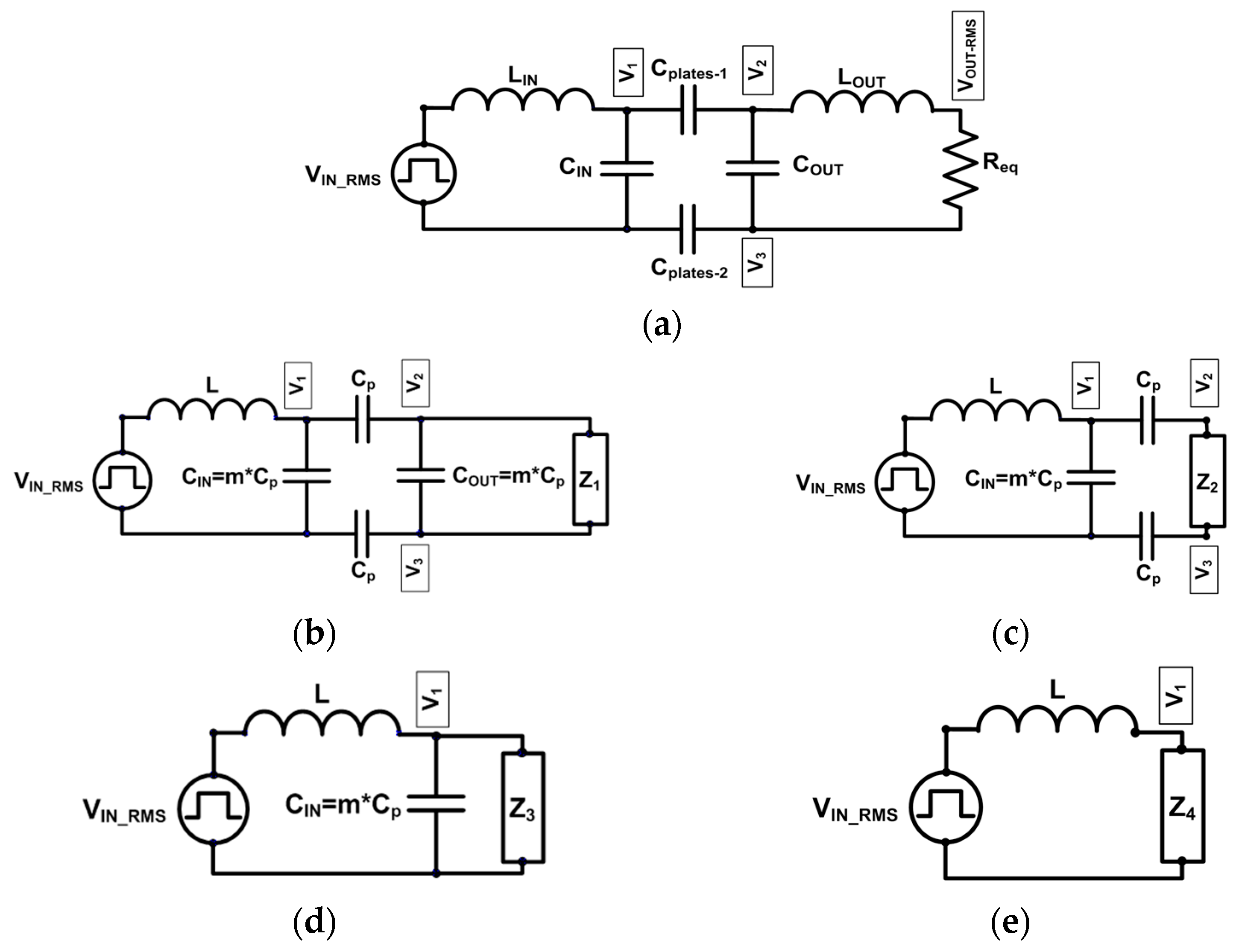
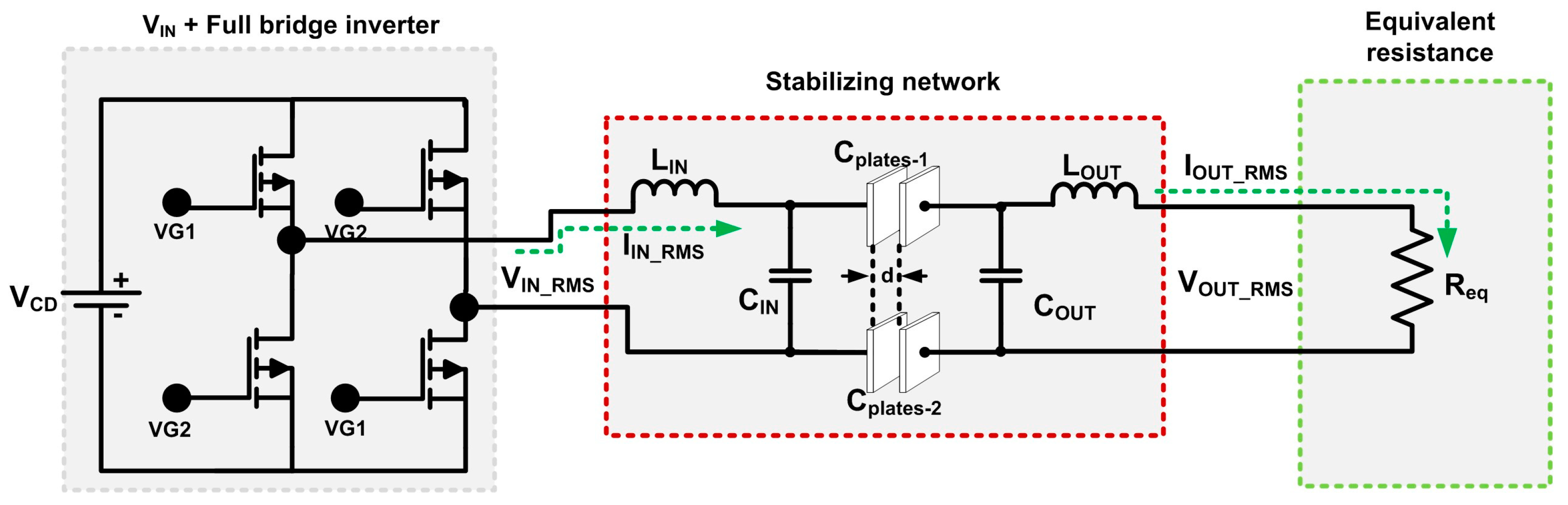
2. Design of Stabilizing Network

2.1. Stabilizing Network Analysis

To achieve a stable coupling between the inverter and the load, a double-sided LC stabilizing network is used. Its design is based on the maximum power transfer, considering a voltage gain (|GVT|) and current gain (|GIT|) close to unity. To stabilize the network first, the low value of the coupling capacitances needs to be compensated so that the system can operate in resonance; secondly, the stability of the system must be maintained in case of variations in the value of the coupling capacitor, caused by changes in the distance between the plates. The complete circuit used for the capacitive wireless transmitter and the main blocks that form the transmitter proposal are shown in Figure 1, where the equivalent load models the rectification, filtering, and output load stage.
Through a series–parallel reduction in the circuit in Figure 1, considering a symmetric stabilizing network that complies with the characteristics LIN = LOUT = L, CIN = COUT = C, and Cplates-1 = Cplates-2 = Cp (where Cplates-1 and Cplates-2 are the coupling capacitors), the expressions for total impedance ( Z T ) and total gains of voltage and current ( G V T and G I T , respectively) are developed as indicated in (6), (9), and (10), respectively, where γ is the normalized resonance frequency, ϕ is the normalized cut-off frequency, and m is the capacitance ratio, as indicated in (3) to (5), respectively. The resonance frequency and cut-off frequency are obtained as indicated in (1) and (2).
f 0 = 1 2 π L C
f c u t o f f = 1 2 π C R e q
γ = f o p e r a t i o n f 0
ϕ = f o p e r a t i o n f c u t o f f
m = C C p
Z T = γ 4 [ 2 m + 2 ] γ 2 [ 4 m + 2 ] + 2 m + j ϕ ( [ 2 m + 1 ] γ 2 [ 2 m + 2 ] ) j ω C ( [ 2 m + 1 ] γ 2 [ 2 m + 2 ] + j ϕ [ 2 m + 2 ] )
Z T ( R e ) = ϕ { ( [ 2 m + 1 ] γ 2 [ 2 m + 2 ] ) 2 ( γ 4 [ 2 m + 2 ] γ 2 [ 4 m + 2 ] + 2 m ) ( 2 m + 2 ) } ω C ( ϕ 2 ( 2 m + 2 ) 2 + ( [ 2 m + 1 ] γ 2 [ 2 m + 2 ] ) 2 )
Z T ( I m ) = ( [ 2 m + 1 ] γ 2 [ 2 m + 2 ] ) ( ϕ 2 [ 2 m + 2 ] + γ 4 [ 2 m + 2 ] γ 2 [ 4 m + 2 ] + 2 m )   ω C ( ϕ 2 ( 2 m + 2 ) 2 + ( [ 2 m + 1 ] γ 2 [ 2 m + 2 ] ) 2 )
| G V T | =           ϕ { γ 4 [ 2 m + 2 ] γ 2 [ 4 m + 2 ] + 2 m } 2 + { ϕ ( [ 2 m + 1 ] γ 2 [ 2 m + 2 ] ) } 2
| G I T | = 1 { [ 2 m + 1 ] γ 2 [ 2 m + 2 ] } 2 + { ϕ [ 2 m + 2 ] } 2
Because the expression of ZT is a complex expression, it is developed to obtain its real and imaginary part ( Z T ( R e ) and Z T ( I m ) , respectively), as indicated in (7) and (8). To operate at a resonance condition, it is necessary that Z T ( I m ) be equal to zero. In order to achieve this condition, the term [ 2 m + 1 ] γ 2 [ 2 m + 2 ] = 0 is used. Developing and substituting the definition of γ , an expression to calculate f o p e r a t i o n is obtained.
f o p e r a t i o n f 0 = γ = 2 m + 1 2 m + 2
By the design condition, f 0 depends on the L I N C I N and L O U T C O U T elements, as indicated in (1). However, (11) also indicates that the resonant frequency of the circuit is affected by the coupling capacitances, being a ratio of f 0 that depends on the capacitance ratio m . In accordance with the above considerations, it can be determined that the resonance frequency of the CPT system agrees with f_operation. Consequently, it can be determined that Z_T(Im) is equal to zero and Z_T(Re) is equal to R_eq (as shown in the Appendix A).
With the magnitude condition of (10) equal to 1, variable ϕ can be obtained as indicated in (12), ensuring the maximum power transfer operation. By substituting (11) into (12) and expanding, (13) is obtained.
ϕ = 1 ( [ 2 m + 1 ] γ 2 [ 2 m + 2 ] ) 2 2 m + 2
ϕ = 1 2 m + 2
By substituting the definitions of ϕ and f c u t o f f into (13), an expression that links the values of resonant capacitors (CIN = COUT = C) and the equivalent load (Req) is obtained, as indicated in (15).
ϕ = f o p e r a t i o n f c u t o f f = 2 π C R e q f o p e r a t i o n = 1 2 m + 2
C R e q = 1 ( 2 m + 2 ) 2 π f o p e r a t i o n
The voltage stress in resonant capacitors is a variable that must be considered because the voltage can reach values of thousands of volts by energizing the circuit with tens of volts, which could damage the components; in addition, the number of discrete capacitors to be used depending on the application must be estimated. With ZT analysis, it is possible to see the behavior of the voltage and current ratio in the input and output capacitors with respect to VIN-RMS and IIN-RMS, as well as the behavior of γ as a function of m , as observed in Figure 2a,b. It can be seen that as m increases, a stability in γ is generated, implying that the resonant frequency of the system is less affected due to changes in the coupling capacitors ( f o p e r a t i o n f 0 ) ; however, the voltage and current in the resonant capacitors increase (by a factor of 2 m + 1 times for voltage in CIN capacitor and by a factor of 2 m times for voltage in COUT capacitor).
In designing the CPT system, it is important to determine the value of m that will ensure stability in the resonant frequency when the coupling capacitors are subject to change, as well as stability in the voltages and currents in the resonant capacitors. From Figure 2, it can be determined that with m = 5 it is possible to operate at 95% of the resonant frequency, and the expected voltage in CIN is approximately eleven times VIN-RMS (this being an important condition for the design).
To obtain the necessary values of the CPT system to operate at maximum power transfer and considering the voltage stress in resonant capacitors, a calculation methodology is presented, which is validated through simulations and experimental results.

2.2. Coupling Capacitances

The design of the experimental prototype is based on a coupling capacitance of 100 pF. To perform the design of the coupling capacitances, a numerical simulation of a 3D model is performed in COMSOL Multiphysics 6.0 software, where a pair of square copper plates is modeled with 1 mm of separation distance, and the plate length is varied to observe the behavior of the capacitance value obtained. Figure 3 shows the 3D model used, while Table 1 registers the capacitance values obtained with respect to different dimensions of the plate.
It can be seen how the capacitance value increases as the size of the plates increases. For the design of this prototype, the dimensions of the copper plates are established to be 10.3 cm × 10.3 cm, obtaining a value of capacitance in simulation of approximately 100 pF. The value of the coupling capacitances is established on the foundation of the feasible geometric configurations that can be fabricated within the laboratory setting.
The copper plates are placed in a structure whose design allows for distance adjustment between them to validate the operation of the CPT system with changes in the value of the coupling capacitor. A 3D CAD rendering of the structure design is shown in Figure 4.

2.3. Proposed Calculation Methodology and Experimental Prototype Calculation

As the capacitance ratio is a determining factor, the calculation methodology begins by considering the following sequence of calculations:
  • The values of Cp, the inverter supply voltage (VCD), the operation frequency of the inverter, and the power at the output (PReq) are determined, and an initial value of m = 5 is used.
  • The RMS value of the fundamental frequency of VIN-RMS is obtained [38].
    V I N R M S = 0.9 V C D
  • Req is obtained by (17) considering VOUT-RMS = VIN-RMS because the system operates at | G V T | = 1 :
    R e q = V O U T R M S 2 P R e q
  • The resonant capacitances (CIN = COUT = C) are calculated according to (15).
  • The closest commercial value of C is selected, and the maximum voltage value at which it operates (VC-Max) is determined.
  • The real value of m is calculated with m = C / C p .
  • Using Figure 2 and the VIN-RMS value, the voltages that will be generated in the CIN and COUT capacitors are estimated. These voltages must meet the following conditions to avoid component damage.
    V C I N ( 2 m + 1 ) V I N R M S < V C M a x
    V C O U T 2 m V I N R M S < V C M a x
  • The normalized resonance frequency ( γ ) and f 0 are calculated with Equation (11).
  • The inductors (LIN = LOUT = L) are obtained with (20) to operate in resonance.
    L = 1 ( 2 π f 0 ) 2 C
Following steps 1 to 9, the values of the elements are obtained, as indicated in Table 2. The value calculated for C is 422.5 pF, and the estimated values of the voltage are 99 V for CIN and 90 V for COUT. The closest commercial value is 470 pF (KEMET brand film capacitors) with a maximum voltage of 200 VRMS (higher than expected voltages).
To validate the proposed methodology, a case study with PReq = 4 W is performed. The impact of the variation in the capacitance Cp is also considered. As illustrated in Figure 5, the CIN capacitor voltage increases as the value m increases. For this reason, a capacitor arrangement is performed for CIN and COUT (two branches connected in parallel with two capacitors connected in series each), where the capacitive value does not change, and the maximum voltage increases to 400 VRMS.

3. Results

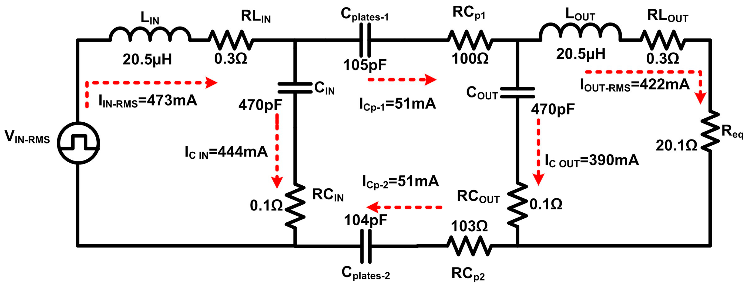
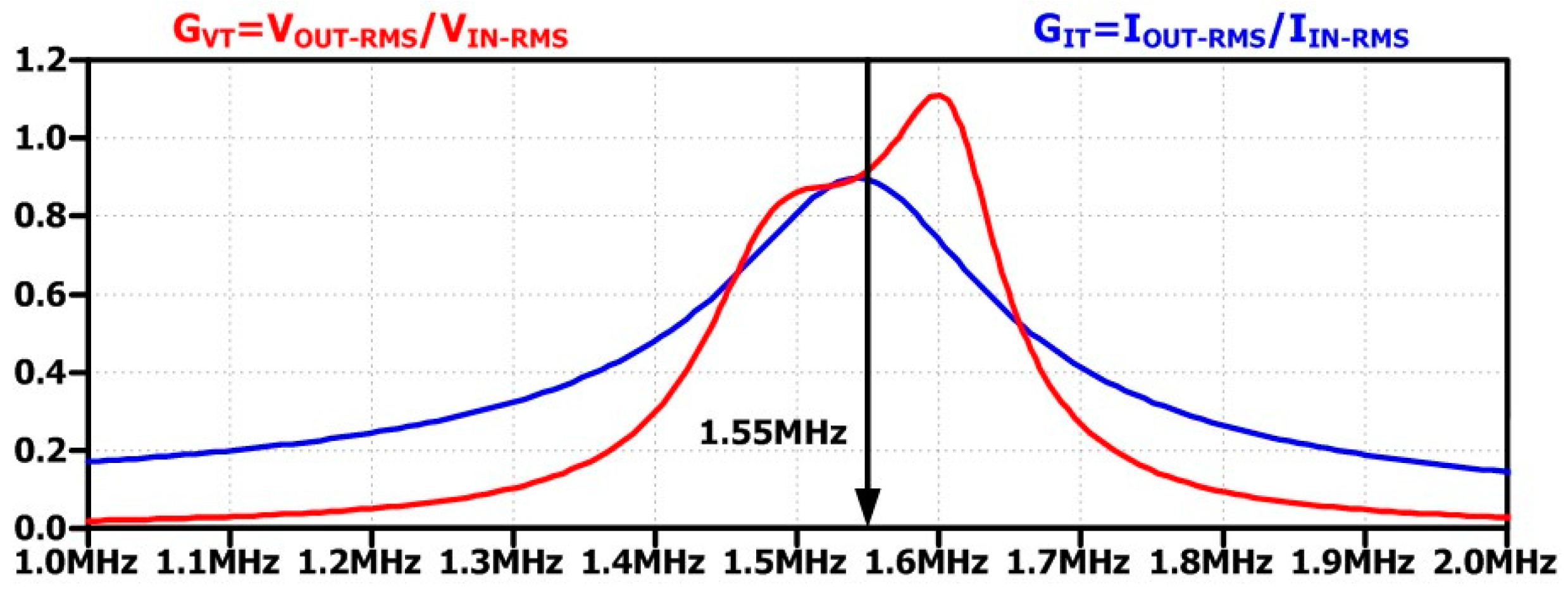
3.1. Simulation Verification

As a first validation of the proposed methodology, a simulation in the frequency domain is performed to verify the equations of voltage and current gains, and a simulation in the time domain is performed to verify the RMS values of the voltage and current at the input and output of the stabilizing network. To obtain more accurate simulation results, the values of the measured parasitic resistances of the reactive elements are considered, as indicated in Figure 6. The parasitic resistances were measured using an impedance meter (model MS5308).
Figure 6 also shows the values of the current flowing through the different elements, as obtained from the simulation. It can be observed that despite the considerable values of R C p 1 and R C p 2 , the associated losses within the circuit are minimal due to the relatively low current flow through the coupling capacitances, which is less than I I N R M S and I O U T R M S .
The simulation results for the voltage and currents gains of the CPT system are shown in Figure 7. The magnitudes obtained are 0.93 and 0.91 for |GVT| and |GIT|, respectively, so it can be observed that the integration of the parasitic resistance has an impact on the gain results, although not significantly.
Waveforms for VIN-RMS and IIN-RMS are shown in Figure 8: the RMS values obtained are 9.97 V and 473 mA, respectively. Figure 9 shows the waveforms for VOUT-RMS and IOUT-RMS: the values obtained are 8.5 V and 422 mA, respectively. In both cases, there is no phase shift between the voltage and current waveforms, indicating that the circuit is operating in resonance. Voltage waveforms for capacitors CIN and COUT are shown in Figure 10, where the RMS values are 96.8 V and 83.6 V, respectively.

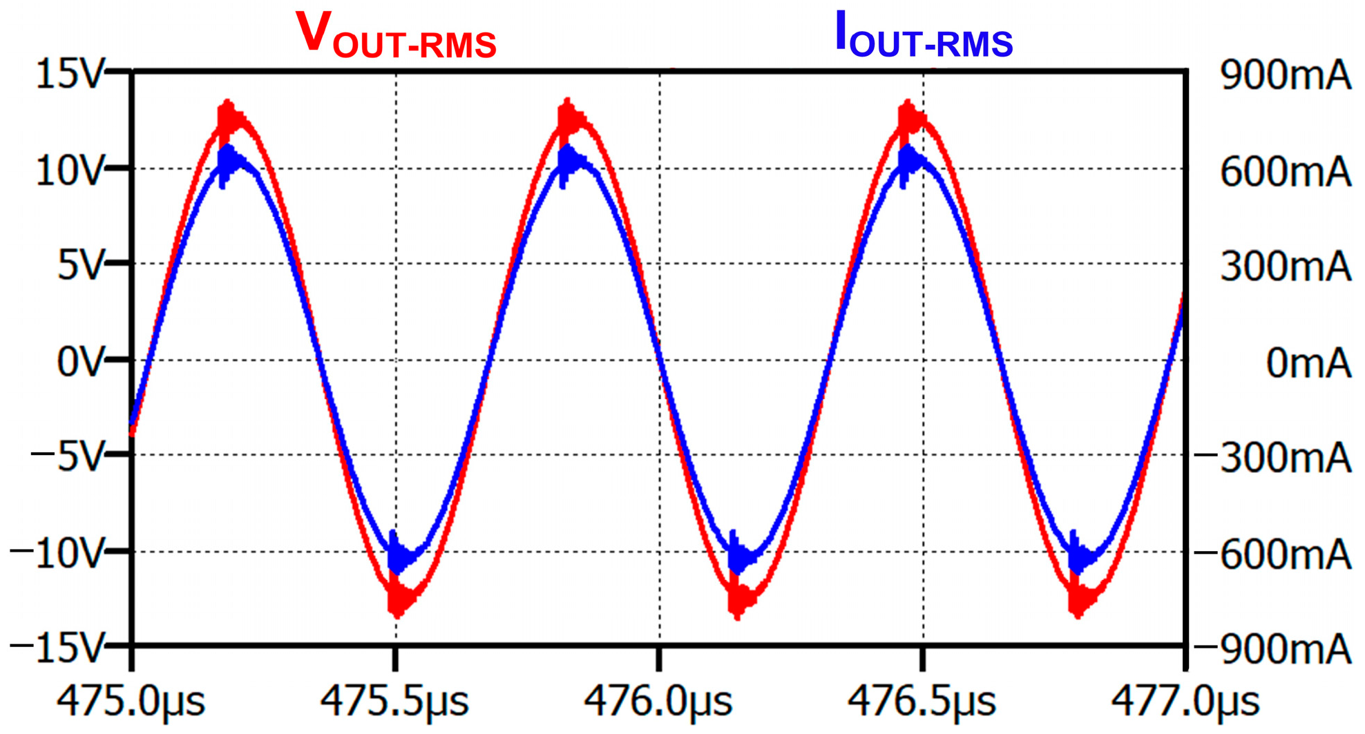
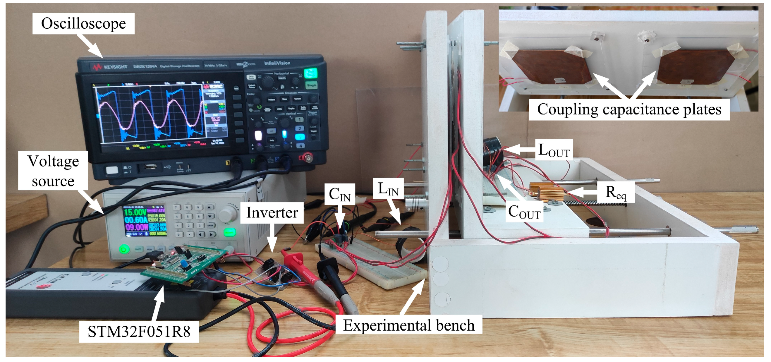
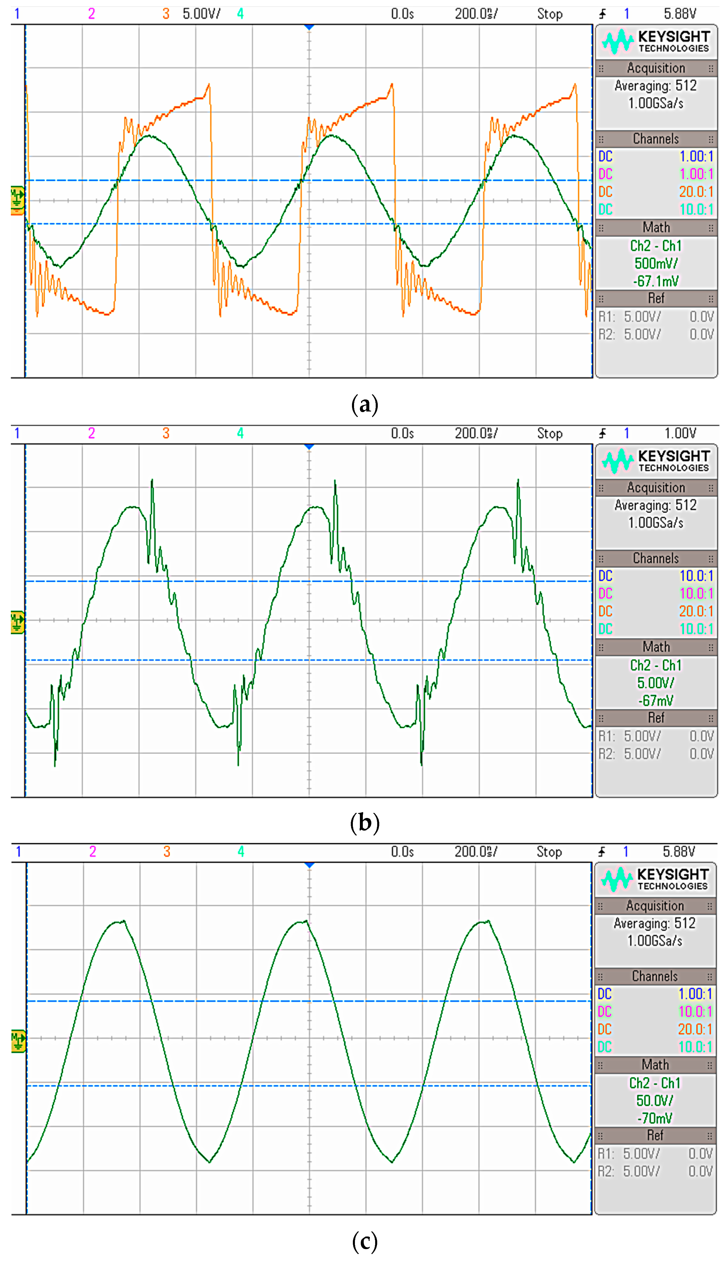
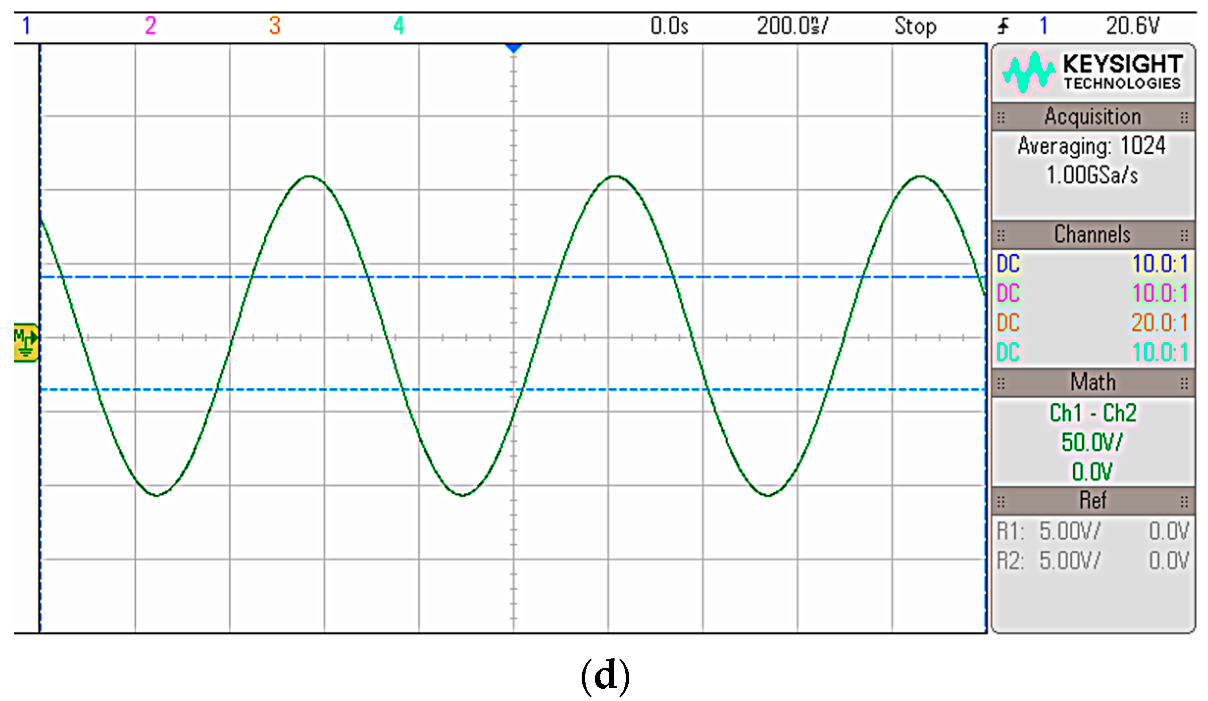
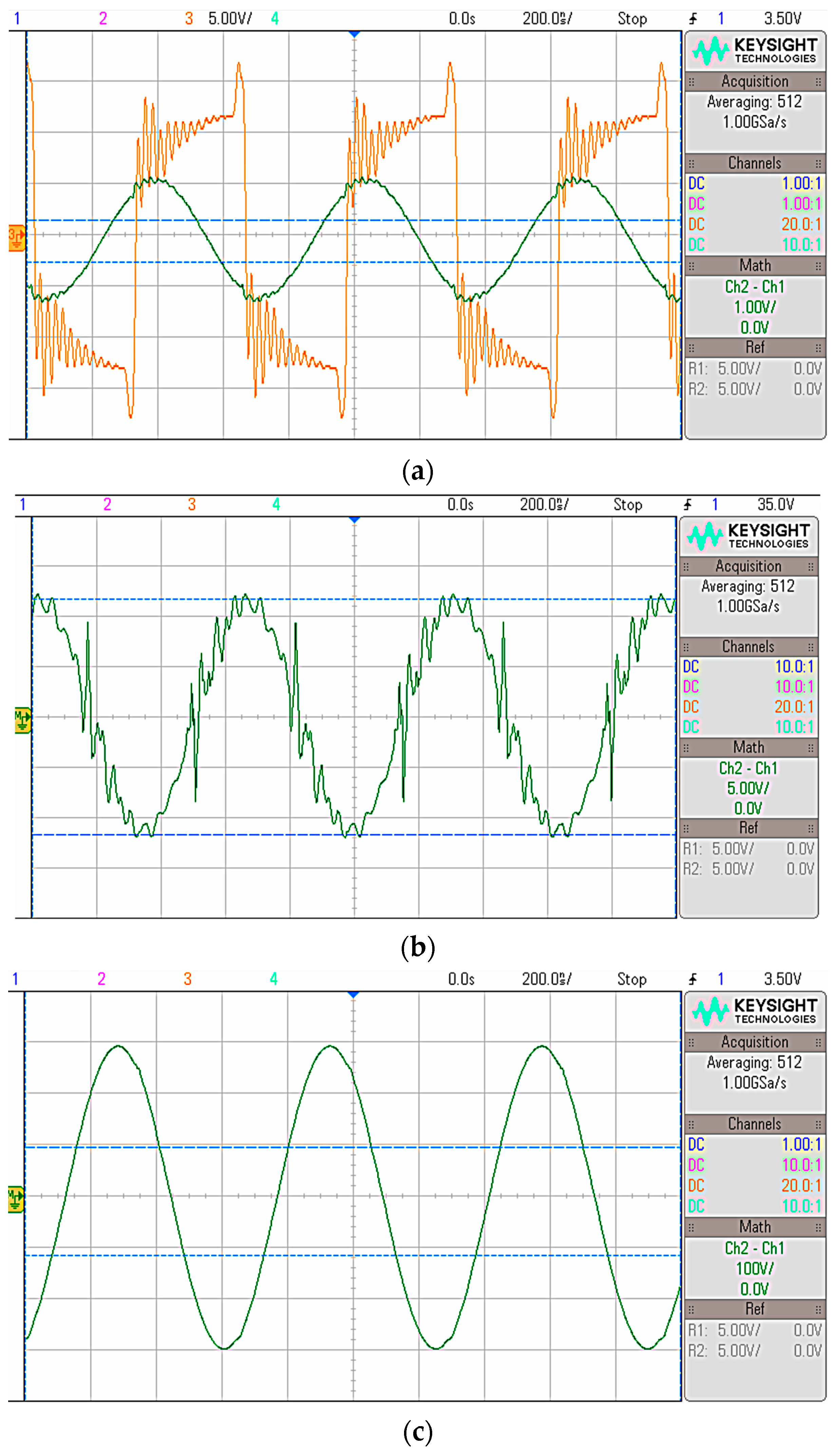
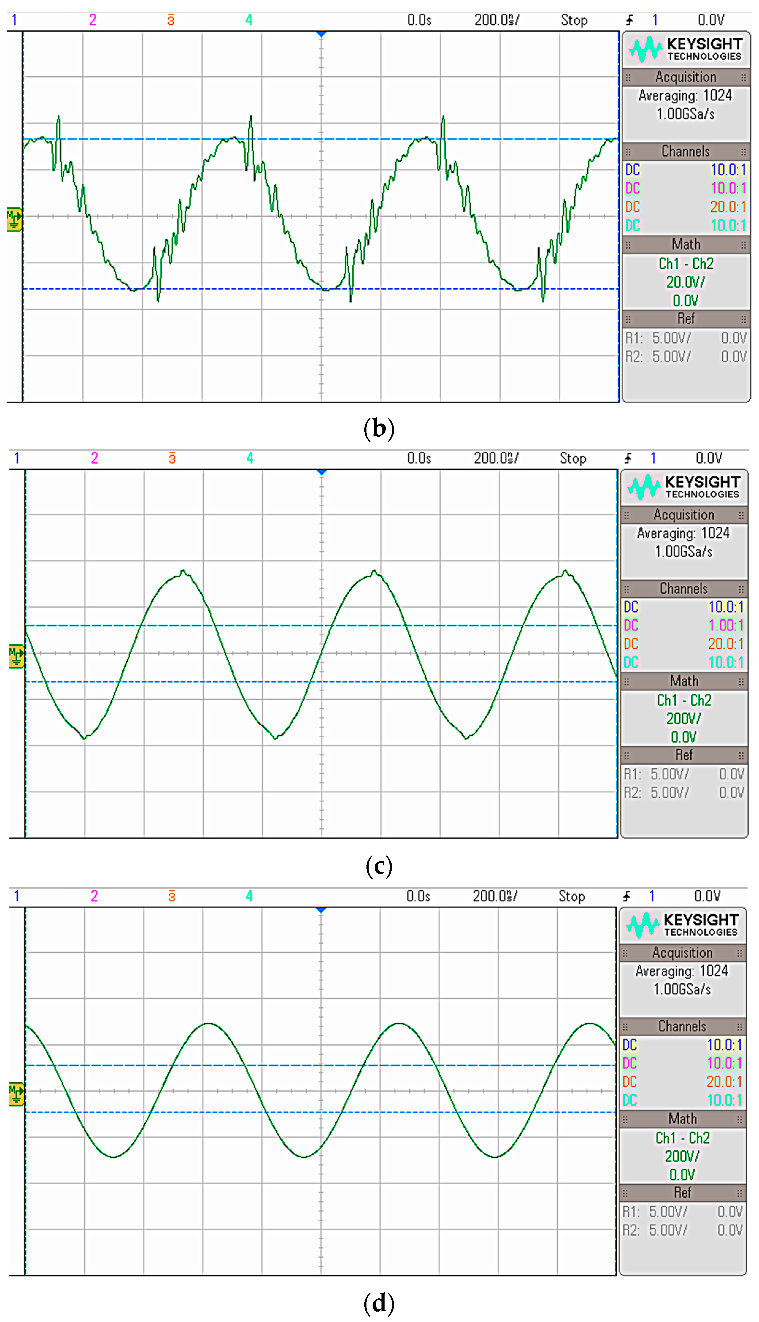
3.2. Experimental Verification

Once the methodology has been verified in simulation, an experimental prototype is performed. An STM32F051R8 microcontroller is used to generate the inverter switching signals, as well as two LMG5200 modules, which are gallium nitride half-bridge inverters. The inductors are produced using 25 mm diameter PVC pipes and AWG 20 magnet wire. For the design of the coupling capacitors, two pairs of 10.3 cm × 10.3 cm copper plates with a thickness of approximately 1.3 mm are used, separated at a distance of approximately 1 mm. The copper plates are placed in a structure whose design allows for distance adjustment between them to validate the operation of the CPT system with changes in the value of the coupling capacitor. Figure 11 shows the prototype used.
Waveforms for VIN-RMS and IIN-RMS are shown in Figure 12a (the IIN-RMS waveform is obtained by using a 1 Ω resistor in series with the LIN inductor). The measured phase shift value is approximately 19°, which indicates that the circuit operates close to resonance. A waveform for VOUT-RMS is shown in Figure 12b, and it can be seen that the waveform is close to a sine wave. Waveforms for the voltages in the CIN and COUT capacitors are shown in Figure 12c,d, respectively.
Table 3 shows the comparison between the expected, simulated, and experimental values. The value for VIN-RMS is obtained with (13) for the theoretical and simulation results, and for the experimental results, function FFT from the oscilloscope is used to measure the RMS voltage at a fundamental frequency of 1.55 MHz. All values of voltages and currents obtained correspond with their RMS value. It can be seen how the values obtained in the simulation and the experimental circuit are similar. Furthermore, they are close to those obtained from the analysis of the development circuit, which validates the proposed design methodology.
A second experiment is performed by varying the separation of the copper plates and monitoring the stability of the system with respect to changes in the value of Cp. As the copper plates were designed at a minimum distance of 1 mm, the experiment consists of increasing that distance, varying the value of Cp from 10 pF in 10 pF steps. Figure 13 and Figure 14 show the waveforms of VIN-RMS, IIN-RMS, VOUT-RMS, V C I N , and V C O U T for two experiments: Cp ≈ 70 pF and Cp ≈ 40 pF, respectively. Table 4 shows the different values for all the experimental results obtained. It can be observed that the CPT system maintains stability in the presence of variations in the value of Cp. This is demonstrated by the maintenance of efficiency at values that are relatively consistent with the initial case. This stability is achieved without the use of a control loop and by maintaining f o p e r a t i o n at a constant value.

3.3. Power Increase

In the proposed calculation methodology, it can be seen that PReq can be increased if VCD increases due to the experimental prototype operating close to the maximum power transfer condition, as can be observed in Table 3, and the principal restriction is the maximum voltage of operation from the capacitors. An experiment to obtain a power increase is developed to transfer 25 W (six times the initial power condition), operating at the minimum distance. To achieve this power, VCD may increase at 25 V, and the expected voltage in capacitor CIN is 234 V approximately, under the 400 V that the capacitor arrangement can operate under. The main waveforms are shown in Figure 15, and a comparison between the expected value and the simulation and experimental results is shown in Table 5.
Table 6 compares the calculation methodology proposed in this paper with previous works. With similar system stabilizing networks, the calculation methodology for a double-sided LC stabilizing network proposed in this paper achieves a high efficiency, controlling the voltage stress in resonant capacitors to avoid damaging them and operating at high frequency.

4. Discussion

The results obtained demonstrate that the proposed stabilizing network’s design methodology effectively stabilizes the voltage and current gains to a value close to 1, as illustrated in Table 4. This is observable when the value of Cp varies from 100 pF to 80 pF, resulting from alterations in the separation of the plates that constitute the coupling capacitance. In response to these variations, the efficiency declines from 82.6% to 80%. This suggests that the system is capable of compensating for changes in the coupling capacitor by operating without a control loop.
Furthermore, the proposal enables a reduction in the voltage stress on the resonant capacitors to a maximum of 245 V/205 V, operating at a power of 23.6 W and an efficiency of 84.7%. This is a lower value than that reported in other similar proposals in the literature, as shown in Table 6.

5. Conclusions

This work proposes a calculation methodology for a stabilizing network to operate at maximum power transfer (prioritizing efficiency), considering the voltage stress in resonant capacitors and maintaining a high efficiency despite changes in the coupling capacitors.
The design methodology proposed in this manuscript allows for the design of a stabilization network based on the value of the coupling capacitance, the requirements of voltage, current, and resonant frequency, and the control of the maximum voltage developed in the resonant capacitors. The methodology has been verified using simulations and experimental validation, with the results for total voltage gain and total current gain being close to unity. This allows for the control of current consumption at the DC source and voltage stability at the load, as well as the application of the CPT system under varying power and frequency conditions. In consideration of practical applications, circumstances that could potentially impact the operation of the CPT system were considered.
As future work, the equivalent series resistance (ESR) of coupling capacitors must be reduced to increase the efficiency of the system. A proposed solution is to make an arrangement in coupling capacitors: instead of using a complete copper plate, the plate could be divided into many segments (m x n matrix) to reduce the ESR value. The results of the simulation and experimentation have demonstrated that parasitic elements, including inductances and capacitances, can introduce distortion into the waveforms. Consequently, it may be beneficial to consider modifications to the connections between the various elements to mitigate this effect. Moreover, the ratio between the values of the capacitors C I N and C O U T and the load (given by the normalized cut-off frequency) must be maintained with the greatest stability possible, as its variation directly affects the efficiency of the circuit as well as the variation in the capacitance ratio. In the case of a potential application in a battery charging system, this characteristic becomes of greater importance, as the impedance of the batteries varies depending on the state of charge. For this reason, a control strategy must be integrated to maintain the stability, and from the analysis of the total impedance, it was observed that the value of the load is a variable that could be controlled to keep the circuit operating close to resonance. However, a more detailed analysis must be performed to verify this hypothesis.

Author Contributions

Conceptualization, E.S.E.-E. and L.H.-G.; methodology, L.H.-G. and J.R.-H.; software, E.S.E.-E. and L.H.-G.; validation, L.H.-G. and J.R.-H.; formal analysis, E.S.E.-E., L.H.-G. and J.R.-H.; investigation, E.S.E.-E., P.G.-L. and O.U.J.-S.; resources, J.R.-H., G.A.A. and O.U.J.-S.; data curation, P.G.-L., J.R.-H. and O.U.J.-S.; writing—original draft preparation, E.S.E.-E. and L.H.-G.; writing—review and editing, J.R.-H. and O.U.J.-S.; visualization, L.H.-G., J.R.-H., G.A.A. and O.U.J.-S.; supervision, L.H.-G.; project administration, L.H.-G., P.G.-L., G.A.A. and J.R.-H.; funding acquisition, L.H.-G. All authors have read and agreed to the published version of the manuscript.

Funding

This research was funded by Instituto Politécnico Nacional (IPN) and Consejo Nacional de Humanidades, Ciencias y Tecnologías (CONAHCyT) of Mexico.

Data Availability Statement

Not applicable. All the necessary information to reproduce the results of this paper is self-contained. In case further information is required, please contact the first author.

Acknowledgments

The authors are grateful to the Instituto Politécnico Nacional (IPN) for their encouragement and kind economic support to realize the research project: SIP 20241563.

Conflicts of Interest

The authors declare no conflicts of interest.

Appendix A

The Z T , G V T , and G I T equations are obtained by a series–parallel reduction in the circuit and the voltage and current divider techniques. The steps of the circuit reduction are shown in Figure A1.
Figure A1. CPT system circuit with series–parallel reduction: (a) Equivalent circuit, (b) Reduction of Req and LOUT form Z1, (c) Z2 represent the reduction of Z1 and COUT, (d) Cp and Z2 in series are reduced to Z3, and (e) Z4 represent the reduction of CIN and Z3 in parallel.
Electronics 13 03859 g0a1
Z 1 = R e q + X L O U T = S L + R e q
Z 2 = X C O U T | | Z 1 = S L + R e q S 2 m L C p + S m C p R e q + 1
Z 3 = X C p 1 + Z 2 + X C p 2 = S 2 L C p [ 2 m + 1 ] + S C p R e q [ 2 m + 1 ] + 2 S 3 m L C p 2 + S 2 m C p 2 R e q + S C p
Z 4 = X C I N | | Z 3 = S 2 L C p [ 2 m + 1 ] + S C p R e q [ 2 m + 1 ] + 2 S 3 L C p 2 [ 2 m 2 + 2 m ] + S 2 C p 2 R e q [ 2 m 2 + 2 m ] + S C p [ 2 m + 1 ]
Z T = X L I N + Z 4 = S 4 L 2 C p 2 [ 2 m 2 + 2 m ] + S 3 L C p 2 R e q [ 2 m 2 + 2 m ] + S 2 L C p [ 4 m + 2 ] + S C p R e q [ 2 m + 1 ] + 2 S 3 L C p 2 [ 2 m 2 + 2 m ] + S 2 C p 2 R e q [ 2 m 2 + 2 m ] + S C p [ 2 m + 1 ]
Considering S = j ω and Equations (A6) and (A7) and the definitions of γ and ϕ , (A5) can be rewritten as indicated in (A8).
f r e s o n a n c e = 1 2 π L C = 1 2 π L m C p
f c u t o f f = 1 2 π C R e q = 1 2 π m C p R e q
Z T = γ 4 [ 2 m + 2 ] γ 2 [ 4 m + 2 ] + 2 m + j ϕ ( [ 2 m + 1 ] γ 2 [ 2 m + 2 ] ) j ω C ( [ 2 m + 1 ] γ 2 [ 2 m + 2 ] + j ϕ [ 2 m + 2 ] )
Since (A8) is a complex equation, it is developed by multiplying by the conjugate of the denominator (as shown in (A9)), thus obtaining the real and imaginary part of the Z T equation, as shown in (A10) and (A11).
Z T = γ 4 [ 2 m + 2 ] γ 2 [ 4 m + 2 ] + 2 m + j ϕ ( [ 2 m + 1 ] γ 2 [ 2 m + 2 ] ) ω C ( ϕ [ 2 m + 2 ] + j ( [ 2 m + 1 ] γ 2 [ 2 m + 2 ] ) ) · ϕ [ 2 m + 2 ] j ( [ 2 m + 1 ] γ 2 [ 2 m + 2 ] ) ϕ [ 2 m + 2 ] j ( [ 2 m + 1 ] γ 2 [ 2 m + 2 ] )
Z T ( R e ) = ϕ { ( [ 2 m + 1 ] γ 2 [ 2 m + 2 ] ) 2 ( γ 4 [ 2 m + 2 ] γ 2 [ 4 m + 2 ] + 2 m ) ( 2 m + 2 ) } ω C ( ϕ 2 ( 2 m + 2 ) 2 + ( [ 2 m + 1 ] γ 2 [ 2 m + 2 ] ) 2 )
Z T ( I m ) = ( [ 2 m + 1 ] γ 2 [ 2 m + 2 ] ) * ( ϕ 2 [ 2 m + 2 ] + γ 4 [ 2 m + 2 ] γ 2 [ 4 m + 2 ] + 2 m )   ω C ( ϕ 2 ( 2 m + 2 ) 2 + ( [ 2 m + 1 ] γ 2 [ 2 m + 2 ] ) 2 )
As the CPT system proposed operates at resonance, Z T ( I m ) is equal to zero (obtaining Equations (11) and (12)), so (A10) is developed to determine the value of Z T ( R e ) under resonance conditions.
Z T ( R e ) = ϕ { [ 2 m + 1 ] 2 2 γ 2 [ 2 m + 2 ] [ 2 m + 1 ] + γ 4 [ 2 m + 2 ] 2 ( γ 4 [ 2 m + 2 ] 2 γ 2 [ 4 m + 2 ] [ 2 m + 2 ] + 2 m [ 2 m + 2 ] ) } ω C ( ϕ 2 ( 2 m + 2 ) 2 + ( [ 2 m + 1 ] γ 2 [ 2 m + 2 ] ) 2 )
Z T ( R e ) = ϕ { [ 2 m + 1 ] 2 2 γ 2 [ 2 m + 2 ] [ 2 m + 1 ] + γ 4 [ 2 m + 2 ] 2 γ 4 [ 2 m + 2 ] 2 + γ 2 [ 4 m + 2 ] [ 2 m + 2 ] 2 m [ 2 m + 2 ] } ω C ( ϕ 2 ( 2 m + 2 ) 2 + ( [ 2 m + 1 ] γ 2 [ 2 m + 2 ] ) 2 )
Z T ( R e ) = ϕ { [ 2 m + 1 ] 2 2 γ 2 [ 4 m 2 + 2 m + 4 m + 2 ] + γ 2 [ 8 m 2 + 8 m + 4 m + 4 ] 2 m [ 2 m + 2 ] } ω C ( ϕ 2 ( 2 m + 2 ) 2 + ( [ 2 m + 1 ] γ 2 [ 2 m + 2 ] ) 2 )
Z T ( R e ) = ϕ { [ 2 m + 1 ] 2 γ 2 [ 8 m 2 + 12 m + 4 ] + γ 2 [ 8 m 2 + 12 m + 4 ] 2 m [ 2 m + 2 ] } ω C ( ϕ 2 ( 2 m + 2 ) 2 + ( [ 2 m + 1 ] γ 2 [ 2 m + 2 ] ) 2 )
Z T ( R e ) = ϕ { [ 2 m + 1 ] 2 2 m [ 2 m + 2 ] } ω C ( ϕ 2 ( 2 m + 2 ) 2 + ( [ 2 m + 1 ] γ 2 [ 2 m + 2 ] ) 2 )
Z T ( R e ) = ϕ { [ 4 m 2 + 4 m + 1 ] [ 4 m 2 + 4 m ] } ω C ( ϕ 2 ( 2 m + 2 ) 2 + ( [ 2 m + 1 ] γ 2 [ 2 m + 2 ] ) 2 )
Z T ( R e ) = ϕ { 1 } ω C ( ϕ 2 ( 2 m + 2 ) 2 + ( [ 2 m + 1 ] γ 2 [ 2 m + 2 ] ) 2 )
Substituting (11) into (A18):
Z T ( R e ) = ϕ ω C ( ϕ 2 ( 2 m + 2 ) 2 + ( [ 2 m + 1 ] ( 2 m + 1 2 m + 2 ) 2 [ 2 m + 2 ] ) 2 )
Z T ( R e ) = ϕ ω C ( ϕ 2 ( 2 m + 2 ) 2 + ( [ 2 m + 1 ] ( 2 m + 1 2 m + 2 ) [ 2 m + 2 ] ) 2 )
Z T ( R e ) = ϕ ω C ( ϕ 2 ( 2 m + 2 ) 2 + ( [ 2 m + 1 ] ( 2 m + 1 ) ) 2 )
Z T ( R e ) = ϕ ω C * ϕ 2 ( 2 m + 2 ) 2
By substituting Equation (13) and the definition of ϕ into (A22), the following result is obtained:
Z T ( R e ) = ϕ 3 ω C * ϕ 2 = ϕ ω C = ω C R e q ω C
Z T ( R e ) = R e q
The result indicated that the value of Z T ( R e ) is equal to R e q .
The equation for G V T is obtained by a series–parallel reduction in the circuit and the voltage divider technique, as shown in Figure A2.
Figure A2. CPT system circuit with series–parallel reduction and voltages nodes: (a) Equivalent circuit with voltage nodes, (b) V2 and V3 are the voltages in COUT and Z1, (c) V2 and V3 are the voltages in Z2, (d) V1 is the voltage in CIN and Z3, and (e) V1 is the voltage in Z4.
Electronics 13 03859 g0a2
V 1 = Z 4 Z T V I N = S 2 L C p [ 2 m + 1 ] + S C p R e q [ 2 m + 1 ] + 2 S 4 L 2 C p 2 [ 2 m 2 + 2 m ] + S 3 L C p 2 R e q [ 2 m 2 + 2 m ] + S 2 L C p [ 4 m + 2 ] + S C p R e q [ 2 m + 1 ] + 2 V I N R M S
V 2 V 3 = Z 2 Z 3 V 1 = S 2 L C p + S C p R e q S 2 L C p [ 2 m + 1 ] + S C p R e q [ 2 m + 1 ] + 2 V 1
By substituting (A25) into (A26), (A27) is obtained.
V 2 V 3 = S 2 L C p + S C p R e q S 4 L 2 C p 2 [ 2 m 2 + 2 m ] + S 3 L C p 2 R e q [ 2 m 2 + 2 m ] + S 2 L C p [ 4 m + 2 ] + S C p R e q [ 2 m + 1 ] + 2 V I N R M S
V O U T R M S = R e q S L + R e q ( V 2 V 3 )
By substituting (A27) into (A28), (A29) is obtained.
V O U T R M S V I N R M S = S C p R e q S 4 L 2 C p 2 [ 2 m 2 + 2 m ] + S 3 L C p 2 R e q [ 2 m 2 + 2 m ] + S 2 L C p [ 4 m + 2 ] + S C p R e q [ 2 m + 1 ] + 2
Considering S = j ω and Equations (A6) and (A7) and the definitions of γ and ϕ , (A29) can be rewritten as indicated in (A30).
G V T = V O U T R M S V I N R M S = j ϕ γ 4 [ 2 m + 2 ] γ 2 [ 4 m + 2 ] + 2 m + j ϕ ( [ 2 m + 1 ] γ 2 [ 2 m + 2 ] )
As the magnitude of GVT is used, it is necessary to develop (A30) to determine its magnitude, as indicated in (A32).
| G V T | = 0 2 + ϕ 2 { γ 4 [ 2 m + 2 ] γ 2 [ 4 m + 2 ] + 2 m } 2 + { ϕ ( [ 2 m + 1 ] γ 2 [ 2 m + 2 ] ) } 2
| G V T | = ϕ { γ 4 [ 2 m + 2 ] γ 2 [ 4 m + 2 ] + 2 m } 2 + { ϕ ( [ 2 m + 1 ] γ 2 [ 2 m + 2 ] ) } 2
The equation for G I T is obtained by a series–parallel reduction in the circuit and the current divider technique, as shown in Figure A3.
Figure A3. CPT system circuit with series–parallel reduction and mesh currents: (a) Equivalent circuit with mesh currents, (b) IOUT-RMS is the current in Z1, (c) I1 is the current in Cp and Z2, (d) I1 is the current in Z3, and (e) IIN-RMS is the current in Z4.
Electronics 13 03859 g0a3
I 1 = X C I N X C I N + Z 3 I I N R M S = S 2 m L C p + S m C p R e q + 1 S 2 L C p [ 2 m 2 + 2 m ] + S C p R e q [ 2 m 2 + 2 m ] + [ 2 m + 1 ] I I N R M S
I O U T R M S = X C O U T X C O U T + Z 1 I 1 = 1 S 2 m L C p + S m C p R e q + 1 I 1
By substituting (A33) into (A34), (A35) is obtained.
I O U T R M S I I N R M S = 1 S 2 L C p [ 2 m 2 + 2 m ] + S C p R e q [ 2 m 2 + 2 m ] + [ 2 m + 1 ]
Considering S = j ω and Equations (A6) and (A7) and the definitions of γ and ϕ , (A35) can be rewritten as indicated in (A36).
G I T = I O U T R M S I I N R M S = 1 [ 2 m + 1 ] γ 2 [ 2 m + 2 ] + j ϕ [ 2 m + 2 ]
As the magnitude of GIT is used, it is necessary to develop (A36) to determine its magnitude, as indicated in (A38).
| G I T | = 1 2 + 0 2 { [ 2 m + 1 ] γ 2 [ 2 m + 2 ] } 2 + { ϕ [ 2 m + 2 ] } 2
| G I T | = 1 { [ 2 m + 1 ] γ 2 [ 2 m + 2 ] } 2 + { ϕ [ 2 m + 2 ] } 2

References

  1. Stankiewicz, J.M. Analysis of the Wireless Power Transfer System Using a Finite Grid of Planar Circular Coils. Energies 2023, 16, 7651. [Google Scholar] [CrossRef]
  2. Lecluyse, C.; Minnaert, B.; Kleemann, M. A Review of the Current State of Technology of Capacitive Wireless Power Transfer. Energies 2021, 14, 5862. [Google Scholar] [CrossRef]
  3. Nguyen, M.T.; Nguyen, C.V.; Truong, L.H.; Le, A.M.; Quyen, T.V.; Masaracchia, A.; Teague, K.A. Electromagnetic Field Based WPT Technologies for UAVs: A Comprehensive Survey. Electronics 2020, 9, 461. [Google Scholar] [CrossRef]
  4. Triviño, A.; González-González, J.M.; Aguado, J.A. Wireless Power Transfer Technologies Applied to Electric Vehicles: A Review. Energies 2021, 14, 1547. [Google Scholar] [CrossRef]
  5. Agarwal, K.; Jegadeesan, R.; Guo, Y.-X.; Thakor, N.V. Wireless Power Transfer Strategies for Implantable Bioelectronics. IEEE Rev. Biomed. Eng. 2017, 10, 136–161. [Google Scholar] [CrossRef]
  6. Park, C.; Park, J.; Shin, Y.; Kim, J.; Huh, S.; Kim, D.; Park, S.; Ahn, S. Separated Circular Capacitive Coupler for Reducing Cross-Coupling Capacitance in Drone Wireless Power Transfer System. IEEE Trans. Microw. Theory Tech. 2020, 68, 3978–3985. [Google Scholar] [CrossRef]
  7. Mahdi, H.; Hoff, B.; Østrem, T. Optimal Solutions for Underwater Capacitive Power Transfer. Sensors 2021, 21, 8233. [Google Scholar] [CrossRef]
  8. Tamura, M.; Murai, K.; Matsumoto, M. Design of Conductive Coupler for Underwater Wireless Power and Data Transfer. IEEE Trans. Microw. Theory Tech. 2021, 69, 1161–1175. [Google Scholar] [CrossRef]
  9. Lu, F.; Zhang, H.; Mi, C. A Two-Plate Capacitive Wireless Power Transfer System for Electric Vehicle Charging Applications. IEEE Trans. Power Electron. 2018, 33, 964–969. [Google Scholar] [CrossRef]
  10. Yi, K. Capacitive Coupling Wireless Power Transfer with Quasi-LLC Resonant Converter Using Electric Vehicles’ Windows. Electronics 2020, 9, 676. [Google Scholar] [CrossRef]
  11. Erfani, R.; Marefat, F.; Mohseni, P. A Dual-Output Single-Stage Regulating Rectifier with PWM and Dual-Mode PFM Control for Wireless Powering of Biomedical Implants. IEEE Trans. Biomed. Circuits Syst. 2020, 14, 1195–1206. [Google Scholar] [CrossRef]
  12. Nag, S.; Koruprolu, A.; Saikh, S.M.; Erfani, R.; Mohseni, P. Auto-Resonant Tuning for Capacitive Power and Data Telemetry Using Flexible Patches. IEEE Trans. Circuits Syst. II Express Briefs 2020, 67, 1804–1808. [Google Scholar] [CrossRef]
  13. Ramos, I.; Afridi, K.; Estrada, J.A.; Popovic, Z. Near-field capacitive wireless power transfer array with external field cancellation. In Proceedings of the IEEE Wireless Power Transfer Conference (WPTC) 2016, Aveiro, Portugal, 5–6 May 2016; pp. 1–4. [Google Scholar]
  14. Regensburger, B.; Sinha, S.; Kumar, A.; Vance, J.; Popovic, Z.; Afridi, K.K. Kilowatt-scale large air-gap multi-modular capacitive wireless power transfer system for electric vehicle charging. In Proceedings of the IEEE Applied Power Electronics Conference and Exposition (APEC) 2018, San Antonio, TX, USA, 4–8 March 2018; pp. 666–671. [Google Scholar]
  15. Zou, L.J.; Hu, A.P. A Contactless Single-Wire CPT (Capacitive Power Transfer) Power Supply for Driving a Variable Message Sign. In Proceedings of the IEEE PELS Workshop on Emerging Technologies: Wireless Power Transfer 2018, Montréal, QC, Canada, 3–7 June 2018; pp. 1–5. [Google Scholar]
  16. Zhang, H.; Lu, F.; Hofmann, H.; Liu, W.; Mi, C. Six-Plate Capacitive Coupler to Reduce Electric Field Emission in Large AirGap Capacitive Power Transfer. IEEE Trans. Power Electron. 2018, 33, 665–675. [Google Scholar] [CrossRef]
  17. Lu, F.; Zhang, H.; Hofmann, H.; Mi, C. A Double-Sided LCLC Compensated Capacitive Power Transfer System for Electric Vehicle Charging. IEEE Trans. Power Electron. 2015, 30, 6011–6014. [Google Scholar] [CrossRef]
  18. Su, Y.-G.; Zhao, Y.-M.; Hu, A.P.; Wang, Z.-H.; Tang, C.-S.; Sun, Y. An F-Type Compensated Capacitive Power Transfer System Allowing for Sudden Change of Pickup. IEEE J. Emerg. Sel. Top. Power Electron. 2018, 7, 1084–1093. [Google Scholar] [CrossRef]
  19. Zhang, H.; Lu, F. An Improved Design Methodology of the Double-Sided LC-Compensated CPT System Considering the Inductance Detuning. IEEE Trans. Power Electron. 2019, 34, 11396–11406. [Google Scholar] [CrossRef]
  20. Mohamed, N.; Aymen, F.; Alqarni, M. Inductive Power Transmission System for Electric Car Charging Phase: Modeling plus Frequency Analysis. World Electr. Veh. J. 2021, 12, 267. [Google Scholar] [CrossRef]
  21. Mohamed, N.; Aymen, F.; Alqarni, M.; Turky, R.A.; Alamri, B.; Ali, Z.M.; Abdel Aleem, S.H.E. A new wireless charging system for electric vehicles using two receiver coils. Ain Shams Eng. J. 2022, 13, 101569. [Google Scholar] [CrossRef]
  22. Wu, X.-Y.; Su, Y.-G.; Hu, A.P.; Zou, L.J.; Liu, Z. A Sleeve-Type Capacitive Power Transfer System With Different Coupling Arrangements for Rotary Application. IEEE Access 2020, 8, 69148–69159. [Google Scholar] [CrossRef]
  23. Liu, Y.; Wu, T.; Fu, M. Interleaved Capacitive Coupler for Wireless Power Transfer. IEEE Trans. Power Electron. 2021, 36, 13526–13535. [Google Scholar] [CrossRef]
  24. Ahmad, S.; Muharam, A.; Hattori, R.; Uezu, A.; Mostafa, T.M. Shielded Capacitive Power Transfer (S-CPT) without Secondary Side Inductors. Energies 2021, 14, 4590. [Google Scholar] [CrossRef]
  25. Huh, S.; Ahn, D. Optimum Receiver-Side Tuning Capacitance for Capacitive Wireless Power Transfer. Electronics 2019, 8, 1543. [Google Scholar] [CrossRef]
  26. Xie, S.; Su, Y.; Zhou, W.; Zhao, Y.; Dai, X. An Electric-Field Coupled Power Transfer System with a Double-sided LC Network. J. Power Electron. 2018, 18, 289–299. [Google Scholar]
  27. Abramov, E.; Zeltser, I.; Peretz, M.M. A network-based approach for modeling resonant capacitive wireless power transfer systems. CPSS Trans. Power Electron. Appl. 2019, 4, 19–29. [Google Scholar] [CrossRef]
  28. Luo, B.; Hu, A.P.; Munir, H.; Zhu, Q.; Mai, R.; He, Z. Compensation Network Design of CPT Systems for Achieving Maximum Power Transfer Under Coupling Voltage Constraints. IEEE J. Emerg. Sel. Top. Power Electron. 2022, 10, 138–148. [Google Scholar] [CrossRef]
  29. Mostafa, T.M.; Bui, D.; Muharam, A.; Hu, A.P.; Hattori, R. Load Effect Analysis and Maximum Power Transfer Tracking of CPT System. IEEE Trans. Circuits Syst. I Regul. Pap. 2020, 67, 2836–2848. [Google Scholar] [CrossRef]
  30. Abramov, E.; Peretz, M.M. Adaptive Self-Tuned Controller IC for Resonant-Based Wireless Power Transfer Transmitters. IEEE Trans. Power Electron. 2021, 36, 12413–12431. [Google Scholar] [CrossRef]
  31. Truong, C.-T.; Choi, S.-J. Single-Stage Duty-Controlled Half-Bridge Inverter for Compact Capacitive Power Transfer System. IEEE Access 2021, 9, 119250–119261. [Google Scholar] [CrossRef]
  32. Sinha, S.; Kumar, A.; Afridi, K.K. Active variable reactance rectifier—A new approach to compensating for coupling variations in wireless power transfer systems. In Proceedings of the 2017 IEEE 18th Workshop on Control and Modeling for Power Electronics (COMPEL), Stanford, CA, USA, 9–12 July 2017; pp. 1–8. [Google Scholar]
  33. Liang, J.; Wu, D.; Yu, J. A Design Method of Compensation Circuit for High-Power Dynamic Capacitive Power Transfer System Considering Coupler Voltage Distribution for Railway Applications. Electronics 2021, 10, 153. [Google Scholar] [CrossRef]
  34. Dai, J.; Hagen, S.S.; Ludois, D.C. High-Efficiency Multiphase Capacitive Power Transfer in Sliding Carriages With Closed-Loop Burst-Mode Current Control. IEEE J. Emerg. Sel. Top. Power Electron. 2019, 7, 1388–1398. [Google Scholar] [CrossRef]
  35. Mai, R.; Luo, B.; Chen, Y.; He, Z. Double-sided CL compensation topology-based component voltage stress optimization method for capacitive power transfer charging system. IET Power Electron. 2018, 11, 1153–1160. [Google Scholar] [CrossRef]
  36. Han, Y.; Perreault, D.J. Analysis and Design of High Efficiency Matching Networks. IEEE Trans. Power Electron. 2006, 21, 1484–1491. [Google Scholar] [CrossRef]
  37. Lu, F.; Zhang, H.; Hofmann, H.; Mi, C.C. A Double-Sided LC Compensation Circuit for Loosely Coupled Capacitive Power Transfer. IEEE Trans. Power Electron. 2018, 33, 1633–1643. [Google Scholar] [CrossRef]
  38. Erickson, R.W.; Maksimović, D. Resonant Conversion. In Fundamentals of Power Electronics, 2nd ed.; Kluwer Academic Publishers: Norwell, MA, USA, 2001; pp. 710–711. [Google Scholar]
  39. Lian, J.; Qu, X. Design of a Double-Sided LC Compensated Capacitive Power Transfer System with Capacitor Voltage Stress Optimization. IEEE Trans. Circuits Syst. II Express Briefs 2020, 67, 715–719. [Google Scholar] [CrossRef]
  40. Qing, X.-D.; Wang, Z.-H.; Su, Y.-G.; Zhao, Y.-M.; Wu, X.-Y. Parameter Design Method With Constant Output Voltage Characteristic for Bilateral LC-Compensated CPT System. IEEE J. Emerg. Sel. Top. Power Electron. 2020, 8, 2707–2715. [Google Scholar] [CrossRef]
  41. Wu, Y.; Chen, Q.; Ren, X.; Zhang, Z. Efficiency Optimization Based Parameter Design Method for the Capacitive Power Transfer System. IEEE Trans. Power Electron. 2021, 36, 8774–8785. [Google Scholar] [CrossRef]
  42. Xiong, Q.; Shao, Y.; Sun, P.; Sun, J.; Rong, E.; Liang, Y. Constant output characteristics and design methodology of double side LC compensated capacitive power transfer. Sci. Rep. 2022, 12, 2663. [Google Scholar] [CrossRef]
Figure 1. Proposed circuit for CPT system operating at 1.55 MHz and resonance at 1.63 MHz.
Electronics 13 03859 g001
Figure 2. Voltage and current gain behavior in resonant capacitors: (a) in CIN capacitor and (b) in COUT capacitor.
Electronics 13 03859 g002
Figure 3. Three-dimensional model used for the coupling design: (a) isometric perspective and (b) lateral perspective.
Electronics 13 03859 g003
Figure 4. Structure design to change separation of copper plates.
Electronics 13 03859 g004
Figure 5. Voltage in CIN considering γ and ϕ constants.
Electronics 13 03859 g005
Figure 6. CPT circuit used for simulations considering measured parasitic resistance.
Electronics 13 03859 g006
Figure 7. Total voltage gain (red trace) and total current gain (blue trace).
Electronics 13 03859 g007
Figure 8. Waveforms for VIN-RMS and IIN-RMS.
Electronics 13 03859 g008
Figure 9. Waveforms for VOUT-RMS and IOUT-RMS.
Electronics 13 03859 g009
Figure 10. Waveforms for V C I N and V C O U T .
Electronics 13 03859 g010
Figure 11. CPT experimental prototype and plates of coupling capacitor.
Electronics 13 03859 g011
Figure 12. Waveforms of experimental results for Cp ≈ 100 pF: (a) VIN-RMS (yellow trace) and IIN-RMS (green trace), (b) VOUT-RMS, (c) V C I N , and (d) V C O U T .
Electronics 13 03859 g012aElectronics 13 03859 g012b
Figure 13. Waveforms of experimental results for Cp ≈ 70 pF: (a) VIN-RMS (yellow trace) and IIN-RMS (green trace), (b) VOUT-RMS, (c) V C I N , and (d) V C O U T .
Electronics 13 03859 g013
Figure 14. Waveforms of experimental results for Cp ≈ 40 pF: (a) VIN-RMS (yellow trace) and IIN-RMS (green trace), (b) VOUT-RMS, (c) V C I N , and (d) V C O U T .
Electronics 13 03859 g014aElectronics 13 03859 g014b
Figure 15. Waveforms of experimental results for P R e q = 25 W: (a) VIN-RMS (yellow trace) and IIN-RMS (green trace), (b) VOUT-RMS, (c) V C I N , and (d) V C O U T .
Electronics 13 03859 g015aElectronics 13 03859 g015b
Table 1. Coupling capacitance values with respect to dimensions of the plate.
Length of the PlateCapacitance Obtained
5 cm × 5 cm25.17 pF
10 cm × 10 cm94.88 pF
20 cm × 20 cm365.7 pF
30 cm × 30 cm818.6 pF
40 cm × 40 cm1.44 nF
50 cm × 50 cm2.25 nF
Table 2. Values of the elements for CPT system.
C p = 100   pF R e q 20   Ω
V C D = 10   V m 4.7
f o p e r a t i o n = 1.55   MHz γ 0.952
P R e q = 4   W f r e s o n a n c e 1.623   MHz
V I N R M S = V O U T R M S = 9   V L 20.5   μ H
Table 3. Comparison of results obtained with expected value.
ParameterExpected ValueSimulationExperimental
V I N R M S 9 V9 V8.6 V
I I N R M S 450 mA473 mA517 mA
V O U T R M S 9 V8.5 V8.6 V
I O U T R M S 450 mA422 mA427 mA
P R e q 4 W3.6 W3.6 W
V C I N 94 V96.8 V95 V
V C O U T 85 V83.6 V76 V
G V T 10.941
G I T 10.90.82
η <100%84.6%82.6%
Table 4. Results obtained from changes in Cp.
C p / m V I N R M S I I N R M S V O U T R M S I O U T R M S G V T G I T V C I N V C O U T θ η
100 pF/4.68.6 V517 mA8.6 V427 mA10.8295 V76 V19°82.6%
90 pF/5.18.5 V567 mA8.8 V437 mA1.030.77106 V77 V20.6°80%
80 pF/5.758.6 V592 mA9.1 V452 mA1.050.76119 V80 V19.5°80%
70 pF/6.68.7 V657 mA9.3 V462 mA1.060.7135 V80 V28.5°75%
60 pF/7.68.8 V757 mA9 V447 mA1.020.59155 V74 V35°60%
50 pF/9.29.12 V857 mA8.8 V437 mA0.960.51183 V64 V46°49%
40 pF/11.59.37 V842 mA8.1 V402 mA0.860.47210 V48 V56°41%
Table 5. Results obtained for power increase.
ParameterExpected ValueSimulationExperimental
V I N R M S 22.5 V22.4 V21.7 V
I I N R M S 1.12 A1.17 A1.28 A
V O U T R M S 22.5 V21 V21.8 V
I O U T R M S 1.12 A1.05 A1.08 A
P R e q 25 W22 W23.6 W
V C I N 234 V243 V245 V
V C O U T 212 V210 V205 V
G V T 10.9371
G I T 10.90.84
η <100%84.7%84.7%
Table 6. Comparison between the proposed methodology and similar CPT systems.
Design of a Double-Sided LC Compensated… [39]Parameter Design Method with Constant Output
Voltage… [40]
Efficiency Optimization Based Parameter Design Method… [41]Constant Output Characteristics
and Design Methodology… [42]
Proposed Methodology
Voltage supply24 V48 V128.68 V58.71 V (COV Mode)/58.82 V (COC Mode)25 V
Frequency200 kHz600 kHz1 MHz300 kHz1.55 MHz
Output powerNot mentioned64.8 W100 W209.56 W (COV Mode)/156.68 W (COC Mode)23.6 W
ηNot mentioned87.9%93.02% 81.23% (COV Mode)/88.46% (COC Mode)84.7%
Voltage stress in capacitors (CIN/COUT)760 V/730 V
(Max.)
Not mentioned772 V/799 V
(RMS value)
Not mentioned245 V/205 V
(RMS value)
Disclaimer/Publisher’s Note: The statements, opinions and data contained in all publications are solely those of the individual author(s) and contributor(s) and not of MDPI and/or the editor(s). MDPI and/or the editor(s) disclaim responsibility for any injury to people or property resulting from any ideas, methods, instructions or products referred to in the content.

