Article

Simple Voltage Balancing Control of Four-Level Inverter

1
Power Science Research Institute, Yunnan Power Grid Co., Ltd., Kunming 650217, China
2
School of Electrical Engineering and Automation, Wuhan University, Wuhan 430072, China
*
Author to whom correspondence should be addressed.
Electronics 2024, 13(19), 3878; https://doi.org/10.3390/electronics13193878
Submission received: 31 August 2024 / Revised: 20 September 2024 / Accepted: 27 September 2024 / Published: 30 September 2024
(This article belongs to the Section Power Electronics)

Abstract

:
Multilevel inverters with improved voltage quality are widely used in applications such as motor control and electric vehicles. The four-level active neutral point clamped (4L-ANPC) inverter effectively meets the demands for high power density and low device voltage stress. However, balancing the capacitor voltage and reducing its low-frequency voltage fluctuation are critical challenges that need to be addressed. To address these challenges, this paper proposes a “variable reference + zero-sequence injection” method that requires only three reference voltage signals to determine the injected zero-sequence components. Particularly, the expression of the midpoint current, regarding the modulation index and phase current amplitude, is theoretically derived. This reveals the fundamental connection between the zero-sequence voltage signal and the midpoint current, providing a theoretical foundation for the zero-sequence injection method in four-level inverters. Subsequently, a simulation model and an experimental platform of the 4L-ANPC inverter were developed to compare and analyze the waveforms of the upper and lower capacitor voltages, phase currents, and line voltages under different modulation methods. Additionally, the upper and lower capacitor voltage waveforms were examined for various modulation indices. The results indicate that as the modulation index increases, the low-frequency voltage fluctuation in the upper and lower capacitor voltages also rises. At a modulation index of 0.95, the “variable reference + zero-sequence injection” method effectively suppresses the fluctuation in the upper and lower capacitor voltages to be no more than 1 V. These experimental findings validate the effectiveness of the proposed method.

1. Introduction

Multilevel converters are known for their superior output voltage quality and reduced voltage variability, making them widely applicable in low-voltage, high-power industrial applications, such as photovoltaic power generation, motor control, and electric vehicles. In this domain, multilevel power converter topologies include the three-level neutral point clamped (3L-NPC) converter [1,2], the three-level active neutral point clamped (3L-ANPC) converter [3,4,5], the four-level active neutral point clamped (4L-ANPC) converter [6,7,8], and the five-level active neutral point clamped (5L-ANPC) converter [9,10,11]. The 3L-NPC, 3L-ANPC, and 5L-ANPC converters are popular due to their lower harmonic distortions compared to traditional two-level converters. However, the 5L-ANPC inverter requires multiple film capacitors in parallel at each phase leg to handle high input current requirement, leading to increased size and cost. The 4L-ANPC inverter, on the other hand, meets the demands for high power density, low device voltage stress, and reduced harmonics. The primary challenge for the 4L-ANPC inverter is balancing the capacitor voltage and reducing the ripple of the midpoint current, as it flows into or out of the DC capacitor.
Voltage imbalance brings in increased voltage stress on MOSFETs and increased harmonics. This issue can be addressed by incorporating additional switched-capacitor resonant circuits [12,13], but this approach inevitably results in increased power loss. So far, only a limited number of balancing control methods have been reported to address this issue. One method is virtual space vector pulse width modulation (VSVPWM), which uses multiple switching states to generate each virtual vector, ensuring an equal average current at each neutral point throughout the switching period [14]. Another approach employs model predictive control (MPC), which balances the system by optimizing a cost function [15,16]. A third technique involves an overlapping carrier modulation scheme, as reported in [8,17,18]. Additionally, a recent solution is the variable carrier-based voltage balancing method, described in [19]. Nonetheless, a simpler voltage balancing control method for implementation in a DSP is still needed. The CBPWM method proposed in [20] compares the three modulating signals to the carrier signal and introduces a PI regulator to control the intermediate capacitor voltage at 1/3 Udc, effectively balancing the upper and lower capacitor voltages. Compared to the virtual vector SVPWM method in [12,13], the CBPWM method in [20] has a shorter computation time and is easier to implement digitally in a DSP. However, a significant drawback of the CBPWM method is its inability to adequately address the imbalance between the upper and lower capacitances. Additionally, there is triple fundamental frequency voltage oscillation on the upper and lower capacitors. In the CBPWM schemes described in [21], two simple PI controllers are utilized: one is designed to balance the middle capacitor voltage, while the other focuses on balancing the upper and lower capacitor voltages. However, the PI regulator does not perform optimally in achieving the desired regulation. To address this, a “variable reference proportional resonant (PR) control-based ZSV injection” method is proposed in [22], which effectively balances the DC-link capacitor voltage and eliminates its ripple. The performance of the DC-link capacitor voltage balancing largely depends on the design of the closed-loop controllers. A new carrier-overlapped pulse width modulation (COPWM) method is proposed in [23], utilizing the volt-second balance principle to achieve natural capacitor voltage balancing. In this process, the COPWM method can increase the switching losses. To address this issue, a composite modulation and voltage balancing method is proposed in [24]. For modulation indices below 0.5, a phase-disposition PWM is used, while for indices above 0.5, a decoupled voltage balancing method based on carrier-overlapped PWM is employed. This approach balances NP voltages across the full modulation index range, while reducing switching losses.
Another common method for balancing DC-link capacitor voltages in NPC inverters is to add a zero-sequence voltage signal to the sinusoidal reference signals. This injected zero-sequence voltage signal modifies the direction and magnitude of the neutral-point (NP) current by adjusting the modulation signal’s duty cycle, thereby influencing the balance and ripple of the DC-link capacitor voltage. Thus, selecting the appropriate injected zero-sequence voltage signal is crucial. In [25], a modified phase-shifted PWM (PS-PWM) method is used to balance the central DC-link capacitor voltages by exploiting redundant switching states. An optimal zero-sequence voltage is injected to simultaneously balance the neutral-point voltage and reduce the common-mode voltage, effectively utilizing the degrees of freedom offered by the redundant voltage vectors. An appropriate amount of zero-sequence voltage is injected into the DC bus reference voltage waveform by modeling the discrete dynamic prediction of the current in [26]. However, the voltage balancing performance of the DC capacitor significantly depends on the model parameter design. While ref. [27] studies the relationship between neutral point currents and output voltage, balancing the upper and lower DC-link capacitor voltages through optimal zero-sequence voltage injection, it does not elucidate the fundamental connection between zero-sequence voltage signal injection and midpoint current flow. Consequently, selecting parameters to effectively suppress low-frequency ripples in DC-link capacitor voltages remains a challenge for four-level inverters.
This article proposes a novel and straightforward method for determining the injected zero-sequence voltage signal by comparing the three reference voltage signals for CBPWM in the four-level NPC inverter. This method eliminates the need for predictive modeling or redundant switching to determine the zero-sequence voltage signal. Theoretical analyses show that the proposed CBPWM method balances the DC-link capacitor voltages and reduces the voltage ripples effectively, a requirement in the existing CBPWM schemes in [28].

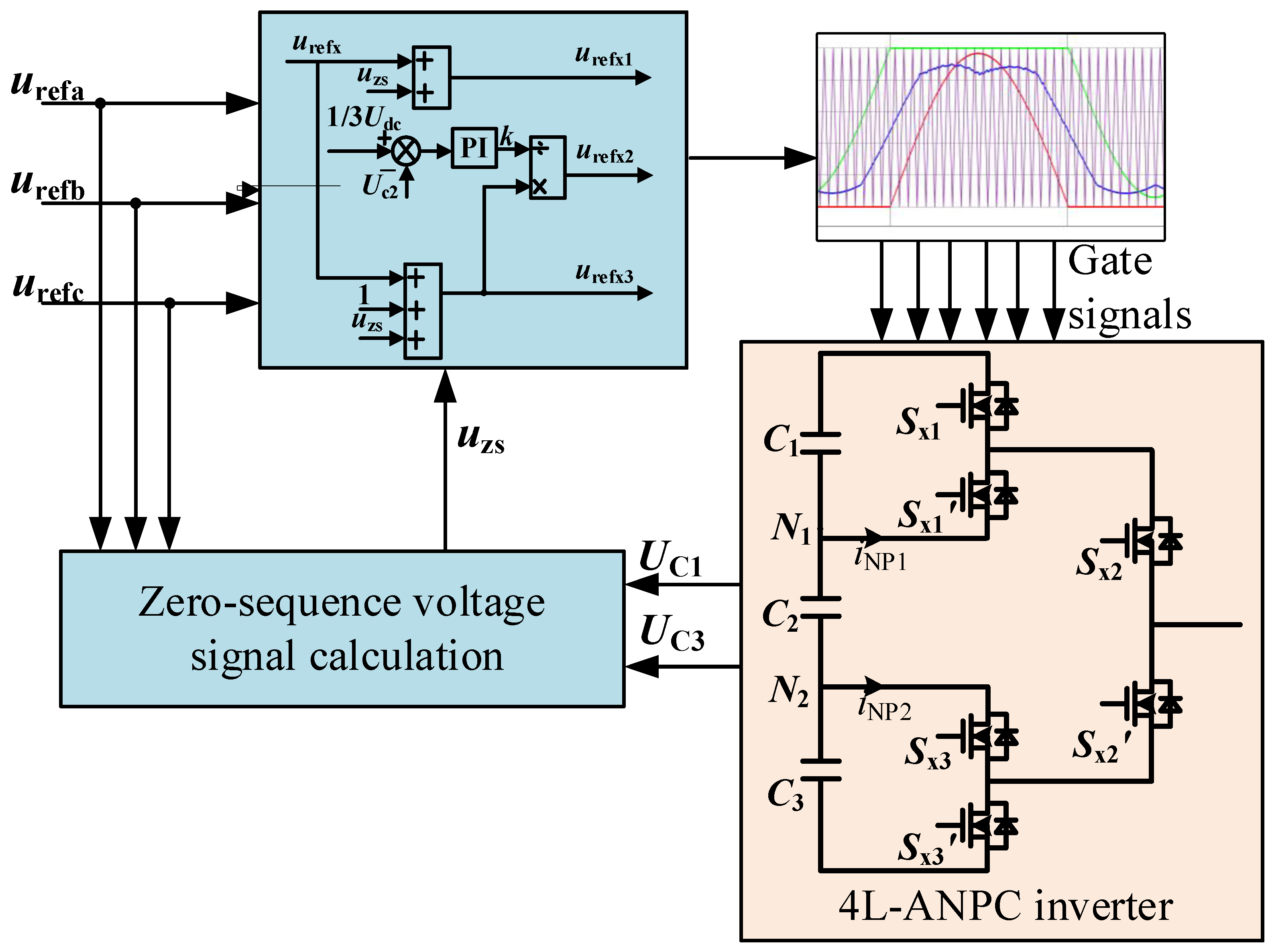
2. Proposed Voltage Balancing Control

The topology of the four-level active neutral-point clamped (4L-ANPC) inverter is illustrated in Figure 1. Assuming that the intermediate capacitor voltage is regulated to 1/3 of the DC bus voltage, each phase capacitor voltage can be controlled to 1/6Udc, allowing the inverter to generate four voltage levels per phase bridge arm. However, the upper and lower capacitor voltages are not inherently balanced.
In the conventional level-shifted carrier modulation scheme, three reference signals urefa, urefb, and urefc are defined by Equation (1):
u ref a = m sin ( 2 π f m t ) u ref b = m sin ( 2 π f m t 2 π 3 ) u ref c = m sin ( 2 π f m t + 2 π 3 )
where m represents the modulation index, and fm denotes the fundamental frequency. Additionally, only one triangular carrier signal Vcarr is utilized with the carrier frequency fs.
The current waveforms of the three phases are defined by Equation (2):
i a = I m sin ( θ φ x ) i b = I m sin ( θ φ x 2 π 3 ) i c = I m sin ( θ φ x + 2 π 3 )
where θ = 2πfmt, and φx (x = a, b, c) is the power factor angle.
A detailed derivation of the capacitor current expression has been carried out in [29] to reveal the mechanism of capacitor voltage imbalance. Briefly, IC1 and IC3 during each fundamental period are influenced by the output current amplitude Im, power factor angle φx, switching angle α, modulation index m, and the DC Idc. In contrast, IC2 is independent of the modulation index m. Furthermore, the amplitude of IC1 is equal to IC3 but greater than IC2. This means that without a voltage balancing circuit or control method, the middle capacitor C2 will be charged less than the other two capacitors. As a result, the capacitor voltage of C2 will eventually discharge to zero, while C1 and C3 equally share the total DC-link voltage, leading to a capacitor voltage imbalance.
As analyzed above, the capacitor voltage imbalance issue of the 4L-ANPC inverter is the over-discharge of the middle capacitor. Balancing the voltage of capacitor C2 at 1/3Udc is crucial. This paper proposes a variable reference voltage balancing method to achieve this. The specific derivation of this method has been presented in [29]. Additionally, to mitigate the voltage fluctuations in the upper and lower DC-link capacitor voltages, the reference voltage is adjusted using a zero-sequence voltage injection method.

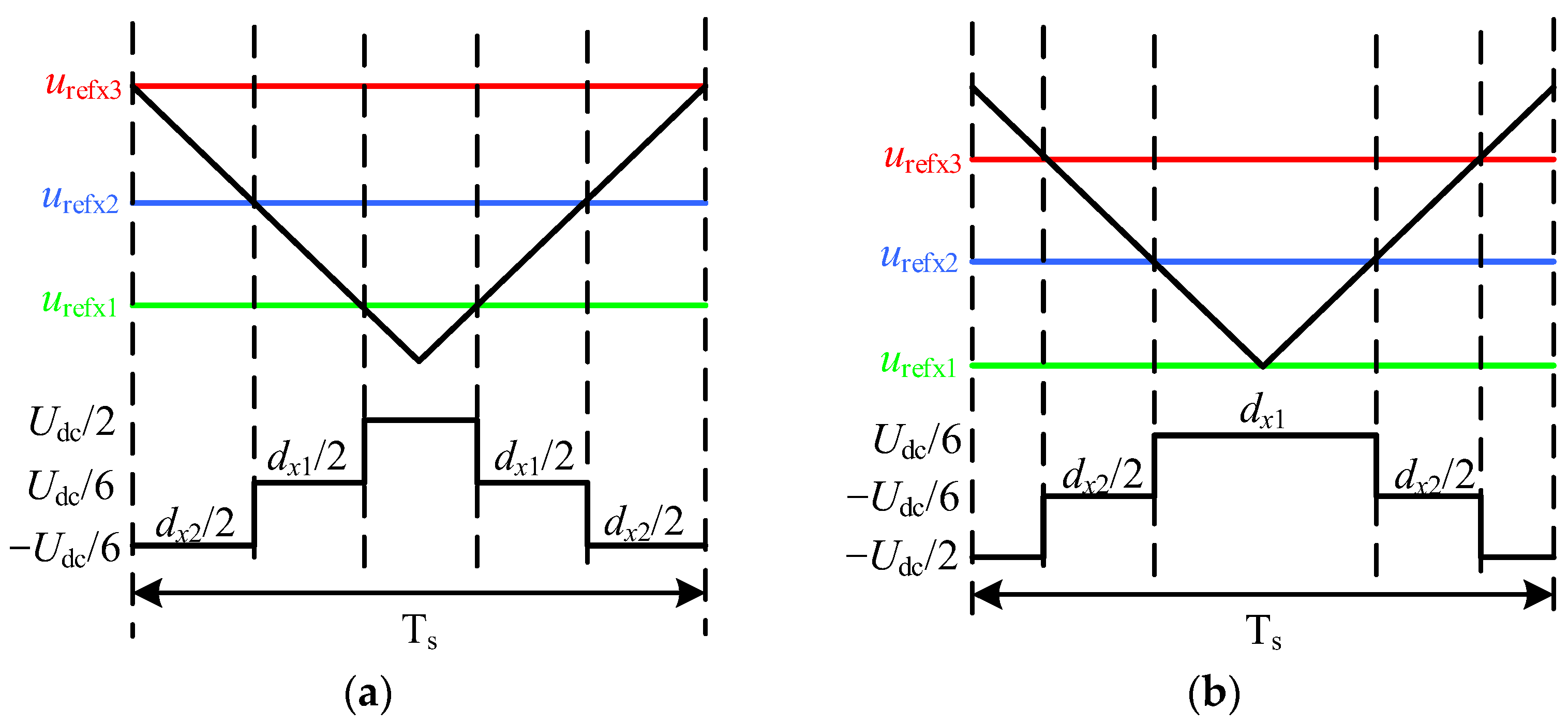
2.1. Variable Reference Voltage Method

The variable reference voltage method is shown in Figure 2. The PI compensator regulates the middle capacitor voltage UC2 to the target value of 1/3Udc with the voltage control error for C2 defined as:
Δ U C 2 = 1 3 U d c U C 2
The three new modulated wave signals urefx (x = a, b, c) are as follows:
u r e f x 1 = u r e f x u r e f x 2 = u r e f x 3 k u r e f x 3 = u r e f x + 1
With the adopted variable reference voltage method, the intermediate capacitor voltage Uc2 can be controlled at 1/3 Udc. Meanwhile, the upper and lower capacitance voltage Uc1 and Uc3 can be automatically balanced due to the symmetry of the proposed four-level converters.

2.2. Zero-Sequence Voltage Injection Method

The zero-sequence voltage signal expression is as follows:
u z s = u z s max = 1 max ( u r e f a , u r e f b , u r e f c ) ,   if   U C 1 U C 3 u z s min = 1 min ( u r e f a , u r e f b , u r e f c ) ,   if   U C 1 < U C 3
where UC1 and UC3 are the voltages of the upper and lower capacitors, respectively.
Three phase modulation signals uxmod (x = a, b, c) are obtained by adding the zero-sequence voltage signal to the reference signal. Then, this modulating signal is compared to the carrier signal to generate a PWM drive signal. The structure of the adopted “variable reference + zero-sequence injection” method is shown schematically in Figure 3. In the figure, the red, blue and green lines represent the three modulated wave signals respectively, and the purple line represents the carrier signal.
u x mod = u r e f x + u z s , x = ( a , b , c )
When the phase current flows through the midpoint N1 (or N2) of the 4L-ANPC inverter, in other words, when the capacitor potential output is Udc/6 or −Udc/6, it causes the DC-link capacitor voltage to be imbalanced. As shown in Figure 4, since the switching frequency is much higher than the fundamental frequency, the reference signal can be regarded as constant in one switching period. The three modulating signals are compared to the carrier signal to obtain the duty cycles for the different levels in one switching cycle.
Since IC1 and IC2 are equal, this paper examines the relationship between the zero-sequence voltage signal injection and midpoint current flow, using midpoint current iN1 as an example.
According to Figure 4, dx1 is denoted as:
d x 1 = d x 2 = 1 u r e f x 2
The average current IN1 in one pulse cycle is denoted as:
i N 1 = ( 1 u a mod 2 ) i a + ( 1 u b mod 2 ) i b + ( 1 u c mod 2 ) i c   = i N 1 _ max ,   if   u z s = u z s _ max i N 1 _ min ,   if   u z s = u z s _ min
According to Equations (5)–(8), it is possible to derive the maximum and minimum values of midpoint currents iN1_max and iN1_min, where k = 0, ±1, ±2…… The expression for the maximum value of the midpoint current is shown in Equations (9)–(11). If 2πfst [2kπ, 2 + π/3] and [2 + 5π/3, 2(k + 1) π], urefa = max (urefa, urefb, urefc), as shown in Equation (9). If 2πfst [2 + π/3, 2 + π], urefb = max (urefa, urefb, urefc), as shown in Equation (10). If 2πfst [2 + π, 2 + 5π/3], urefc = max (urefa, urefb, urefc), as shown in Equation (11).
i N 1 _ max = 3 I m 4 m cos ( φ ) ,    m 1 3 , 2 π f s t [ 2 k π , 2 k π + π 3 ]   and   [ 2 k π + 5 π 3 , 2 ( k + 1 ) π ]   I m 4 [ 2 3 m sin ( 4 π f s t φ ) + 4 cos ( 2 π f s t φ + π 3 ) 3 m sin ( φ ) ] ,           m > 1 3 , 2 π f s t [ 2 k π + 5 π 3 , θ 1 ] , θ 1 = 2 k π + π 6 arccos ( 1 3 m ) I m 4 [ 4 cos ( 2 π f s t φ ) 3 m cos ( φ ) ] ,           m > 1 3 , 2 π f s t [ 2 k π , θ 2 ]   and   [ θ 1 , 2 ( k + 1 ) π ] ,   θ 2 = 2 k π + 11 π 6 + arccos ( 1 3 m ) I m 4 [ 2 3 m sin ( 4 π f s t φ ) + 4 cos ( 2 π f s t φ ) + 3 m sin ( φ ) ] ,           m > 1 3 , 2 π f s t [ θ 2 , 2 k π + π 3 ]
i N 1 _ max = 3 I m 4 m cos ( φ ) ,    m 1 3 , 2 π f s t [ 2 k π + π 3 , 2 k π + π ] I m 4 [ 2 3 m sin ( 4 π f s t φ + 2 π 3 ) + 4 cos ( 2 π f s t φ π 3 ) 3 m sin ( φ ) ] ,           m > 1 3 , 2 π f s t [ 2 k π + π 3 , θ 1 + 2 π 3 ] , θ 1 = 2 k π + π 6 arccos ( 1 3 m ) I m 4 [ 4 cos ( 2 π f s t φ 2 π 3 ) 3 m cos ( φ ) ] ,           m > 1 3 , 2 π f s t [ θ 1 + 2 π 3 , θ 2 + 2 π 3 ] , θ 2 = 2 k π + 11 π 6 + arccos ( 1 3 m ) I m 4 [ 2 3 m sin ( 4 π f s t φ + 2 π 3 ) + 4 cos ( 2 π f s t φ π ) + 3 m sin ( φ ) ] ,           m > 1 3 , 2 π f s t [ θ 2 + 2 π 3 , π ]
i N 1 _ max = 3 I m 4 m cos ( φ ) ,    m 1 3 , 2 π f s t [ 2 k π + π , 2 k π + 5 π 3 ] I m 4 [ 2 3 m sin ( 4 π f s t φ + 4 π 3 ) + 4 cos ( 2 π f s t φ + π ) 3 m sin ( φ ) ] ,           m > 1 3 , 2 π f s t [ 2 k π + π , θ 1 + 4 π 3 ] , θ 1 = 2 k π + π 6 arccos ( 1 3 m ) I m 4 [ 4 cos ( 2 π f s t φ + 2 π 3 ) 3 m cos ( φ ) ] ,           m > 1 3 , 2 π f s t [ 2 k π , θ 2 ]   and   [ θ 1 + 4 π 3 , θ 2 + 4 π 3 ] , θ 2 = 2 k π + 11 π 6 + arccos ( 1 3 m ) I m 4 [ 2 3 m sin ( 4 π f s t φ + 4 π 3 ) + 4 cos ( 2 π f s t φ + π 3 ) + 3 m sin ( φ ) ] ,           m > 1 3 , 2 π f s t [ θ 2 + 4 π 3 , 2 k π + 5 π 3 ]
The expression for the minimum value of the midpoint current is shown in Equations (12)–(14). If 2πfst [2, 2 + 2π/3], urefc = min (urefa, urefb, urefc), as shown in Equation (12). If 2πfst [2 + 2π/3, 2 + 4π/3], urefa = min (urefa, urefb, urefc), as shown in Equation (13). If 2πfst [2 + 4π/3, 2(k + 1) π], urefb = min (urefa, urefb, urefc), as shown in Equation (14).
i N 1 _ min = 3 I m 4 m cos ( φ ) ,     m 1 3 , 2 π f s t [ 2 k π , 2 k π + 2 π 3 ]   I m 4 [ 2 3 m sin ( 4 π f s t φ 2 π 3 ) + 4 cos ( 2 π f s t φ ) 3 m sin ( φ ) ] ,           m > 1 3 , 2 π f s t [ 2 k π , θ 3 ] , θ 3 = 2 k π + π 2 arccos ( 1 3 m ) I m 4 [ 4 cos ( 2 π f s t φ π 3 ) 3 m cos ( φ ) ] ,           m > 1 3 , 2 π f s t [ θ 3 , θ 4 ] , θ 4 = 2 k π + π 6 + arccos ( 1 3 m ) I m 4 [ 2 3 m sin ( 4 π f s t φ 2 π 3 ) + 4 cos ( 2 π f s t φ 2 π 3 ) + 3 m sin ( φ ) ] ,           m > 1 3 , 2 π f s t [ θ 4 , 2 k π + 2 π 3 ]
i N 1 _ min = 3 I m 4 m cos ( φ ) ,     m 1 3 , 2 π f s t [ 2 k π + 2 π 3 , 2 k π + 4 π 3 ] I m 4 [ 2 3 m sin ( 4 π f s t φ ) + 4 cos ( 2 π f s t φ ) 3 m sin ( φ ) ] ,           m > 1 3 , 2 π f s t [ 2 k π + 2 π 3 , θ 3 + 2 π 3 ] , θ 3 = 2 k π + π 2 arccos ( 1 3 m ) I m 4 [ 4 cos ( 2 π f s t φ π ) 3 m cos ( φ ) ] ,           m > 1 3 , 2 π f s t [ θ 3 + 2 π 3 , θ 4 + 2 π 3 ] , θ 4 = 2 k π + π 6 + arccos ( 1 3 m ) I m 4 [ 2 3 m sin ( 4 π f s t φ ) + 4 cos ( 2 π f s t φ 4 π 3 ) + 3 m sin ( φ ) ] ,           m > 1 3 , 2 π f s t [ θ 4 + 2 π 3 , 2 k π + 4 π 3 ]
i N 1 _ min = 3 I m 4 m cos ( φ ) ,     m 1 3 , 2 π f s t [ 2 k π + 4 π 3 , 2 ( k + 1 ) π ] I m 4 [ 2 3 m sin ( 4 π f s t φ + 2 π 3 ) + 4 cos ( 2 π f s t φ + 2 π 3 ) 3 m sin ( φ ) ] ,           m > 1 3 , 2 π f s t [ 2 k π + 4 π 3 , θ 3 + 4 π 3 ] , θ 3 = 2 k π + π 2 arccos ( 1 3 m ) I m 4 [ 4 cos ( 2 π f s t φ + π 3 ) 3 m cos ( φ ) ] ,           m > 1 3 , 2 π f s t [ θ 3 + 4 π 3 , θ 4 + 4 π 3 ] , θ 4 = 2 k π + π 6 + arccos ( 1 3 m ) I m 4 [ 2 3 m sin ( 4 π f s t φ + 2 π 3 ) + 4 cos ( 2 π f s t φ ) + 3 m sin ( φ ) ] ,           m > 1 3 , 2 π f s t [ θ 4 + 4 π 3 , 2 ( k + 1 ) π ]
The relationship between the DC-link capacitor voltage ripple and midpoint current is:
Δ U N = 1 3 C i N 1 d t
where C is the capacitance value of the DC-link capacitor. When the 4L-ANPC inverter operates normally, iN1 is iN1_max or iN1_min. Therefore, when ΔUN is zero:
i N P _ min 0   and   i N P _ max 0
According to Equations (9)–(14), when m 1 3 , iN1_max and iN1_min are both DC components, and iN1_max ≤ 0, iN1_min ≥ 0. Therefore, there is no low-frequency ripple in the DC-link capacitor voltage in this modulation index. When m > 1 3 , there are AC components and DC components for both iN1_max and iN1_min. Taking the example of 2πfst [π/3,π], when 2 π f s t [ 2 k π + π 3 , θ 1 + 2 π 3 ] in the iN1_max expression, this corresponds to segments 2 π f s t [ θ 4 , 2 k π + 2 π 3 ] and 2 π f s t [ 2 k π + 2 π 3 , θ 3 + 2 π 3 ] in the iN1_min expression. Replacing 2πfst in the iN1_max expression with 2πfst-π/3, when 2 π f s t [ 2 k π + 2 π 3 , θ 3 + 2 π 3 ]  iN1_max = −iN1_min, the fundamental frequency of its AC component is 3fs. However, when 2 π f s t [ θ 4 , 2 k π + 2 π 3 ] , iN1_max is not equal to −iN1_min, the ripple of this segment cannot be eliminated. For the same reason, when 2 π f s t [ θ 1 + 2 π 3 , θ 2 + 2 π 3 ] in the iN1_max expression, corresponding to segments 2 π f s t [ θ 3 + 4 π 3 , θ 4 + 4 π 3 ] in the iN1_min expression, the ripple of this segment can also eliminated, while the other segments cannot be. When 2 π f s t [ θ 2 + 2 π 3 , π ] in the iN1_max expression, corresponding to segments 2 π f s t [ θ 4 + 2 π 3 , 2 k π + 4 π 3 ] in the iN1_min expression, the ripple can be eliminated. Therefore, most of the ripple can be eliminated during the whole cycle, and other parts of the ripple can only be weakened, and with the increase in the modulation index, the capacitance voltage ripple amplitude will also increase.

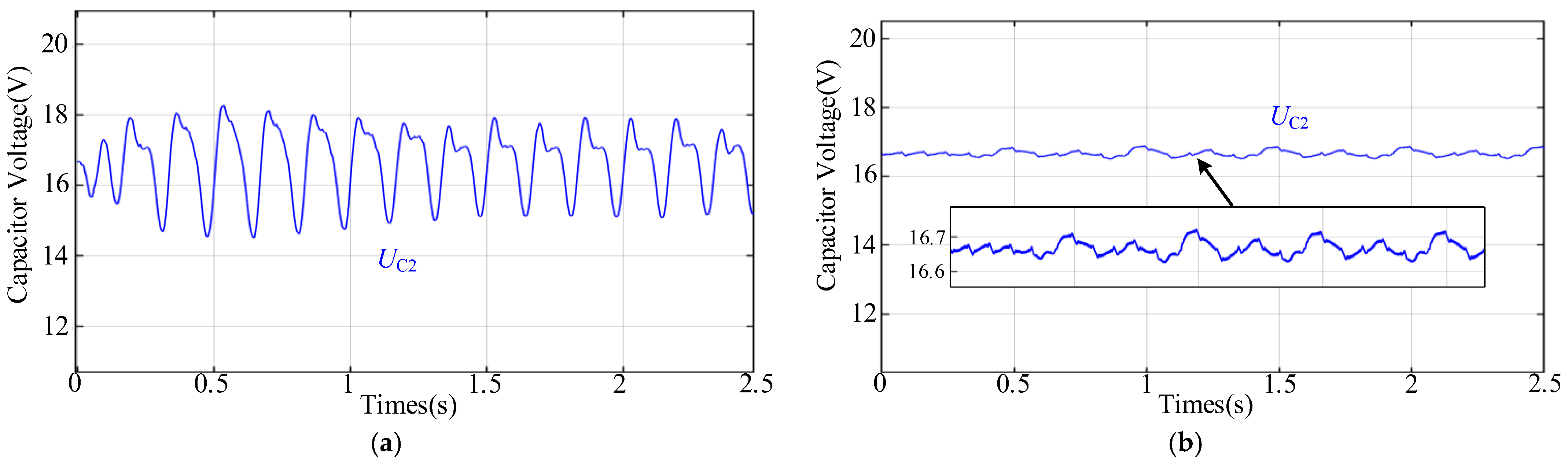
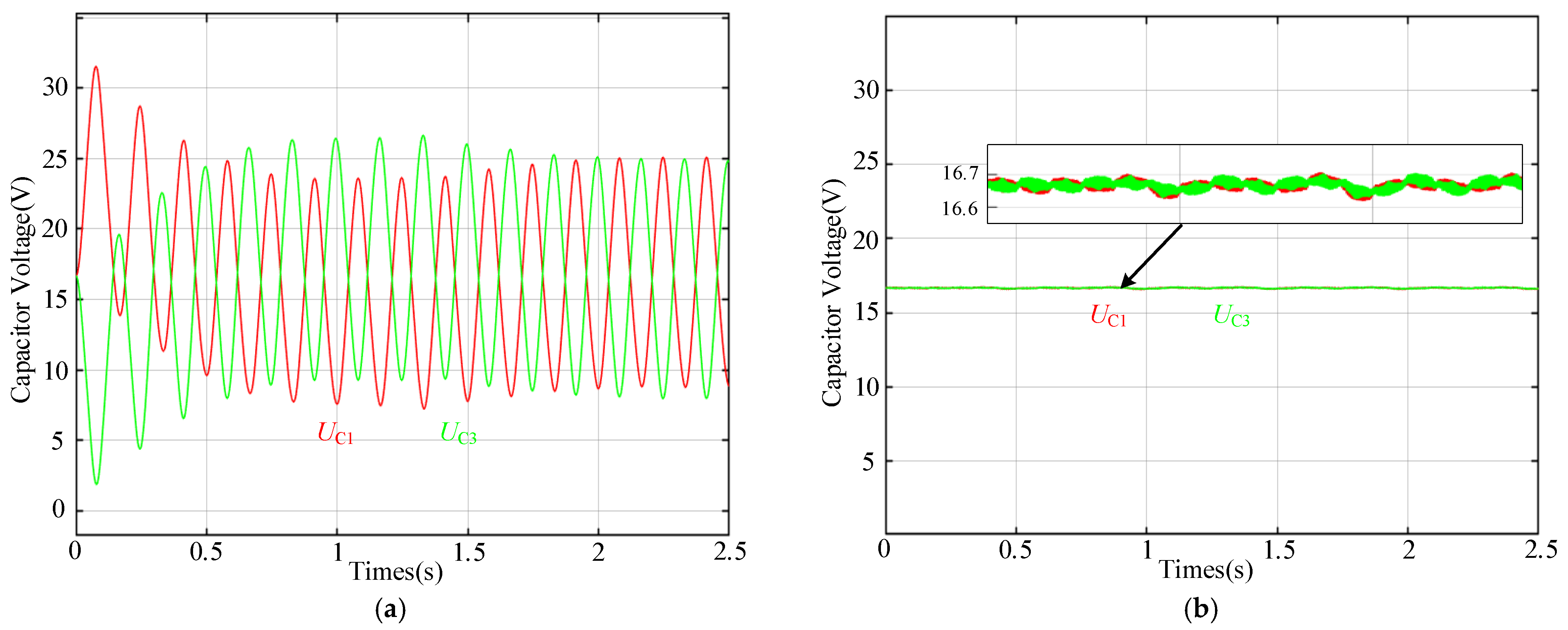
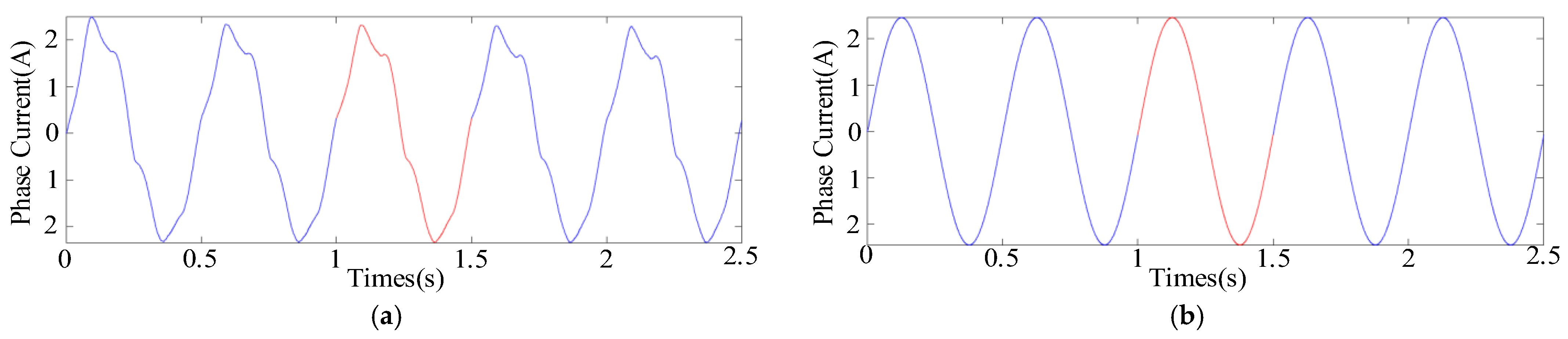
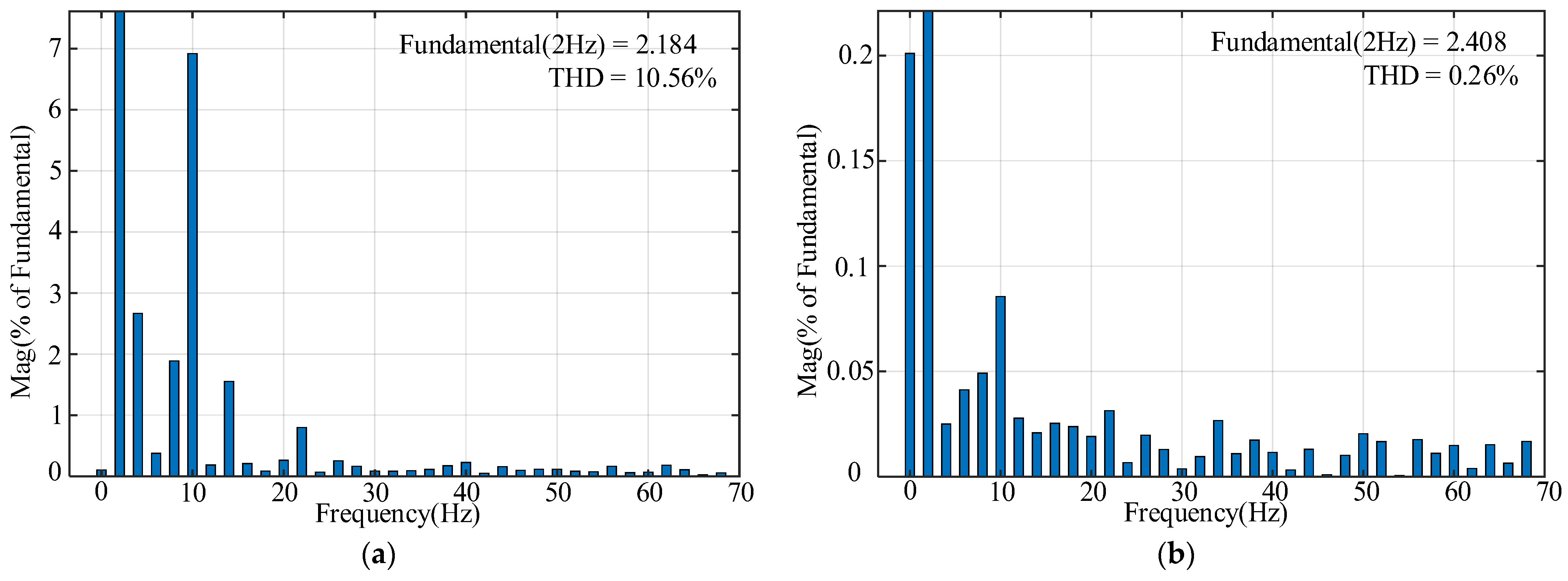
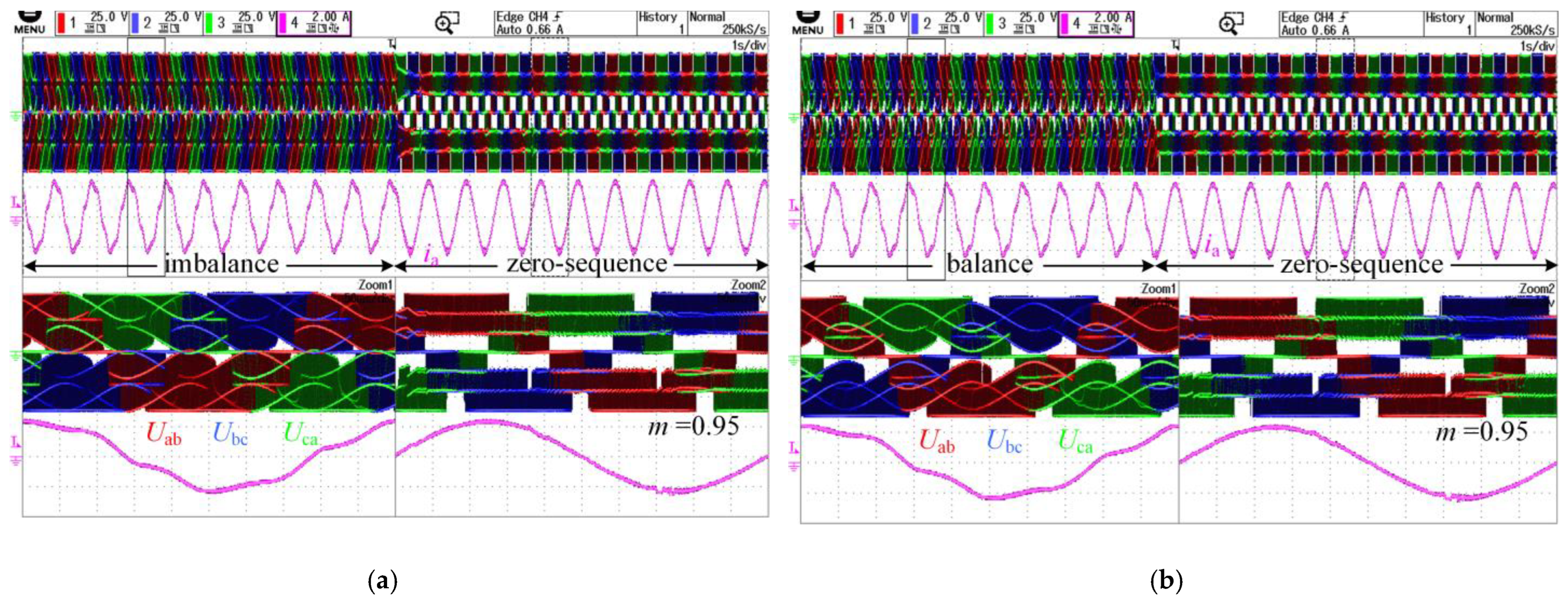
3. Analysis of Simulation Results

A simulation model of the 4L-ANPC inverter has been developed using Matlab/Simulink to validate the proposed “variable reference + zero-sequence injection” method. The specifications for the 4L-ANPC inverter are detailed in Table 1. Figure 5 presents the modulating waveform for the variable reference voltage balancing method, along with the resulting PWM switching signal.
With the application of the “variable reference” voltage balancing method, the capacitor voltage of the 4L-ANPC inverter is maintained at 50 V. Key simulation results for the 4L-ANPC inverter are illustrated in Figure 6 and Figure 7, with a modulation index of 0.95. The intermediate capacitor voltage UC2 is stabilized at 16.7 V, which is 1/3 of the DC-link voltage, verifying the effectiveness of the “variable reference” voltage balancing method. However, the voltage ripple is up to about 10 V for the upper and lower capacitors, and the intermediate capacitor voltage ripple is up to 1 V. This is high for a DC-link voltage of only 50 V. When the “variable reference + zero-sequence injection” method is used, the upper and lower capacitor voltage ripple is less than 0.1 V, and the voltage ripple of the intermediate capacitor is around 0.1 V. It is demonstrated that the variable reference + zero-sequence injection method is more effective in suppressing the low-frequency ripple of the capacitor voltage.
The phase current and its FFT analysis using the “variable reference” method are presented in Figure 8a and Figure 9a. The red line indicates the current analyzed for one cycle. The phase current exhibits a fundamental frequency of 2 Hz, with significant waveform distortion, resulting in a total harmonic distortion (THD) of 10.56%. When the “variable reference + zero-sequence injection” method is used, the waveform is a standard sinusoidal waveform, with a THD of 0.26%, as shown in Figure 9b. This shows that the “variable reference + zero-sequence injection” method has a better effect in improving phase current THD.

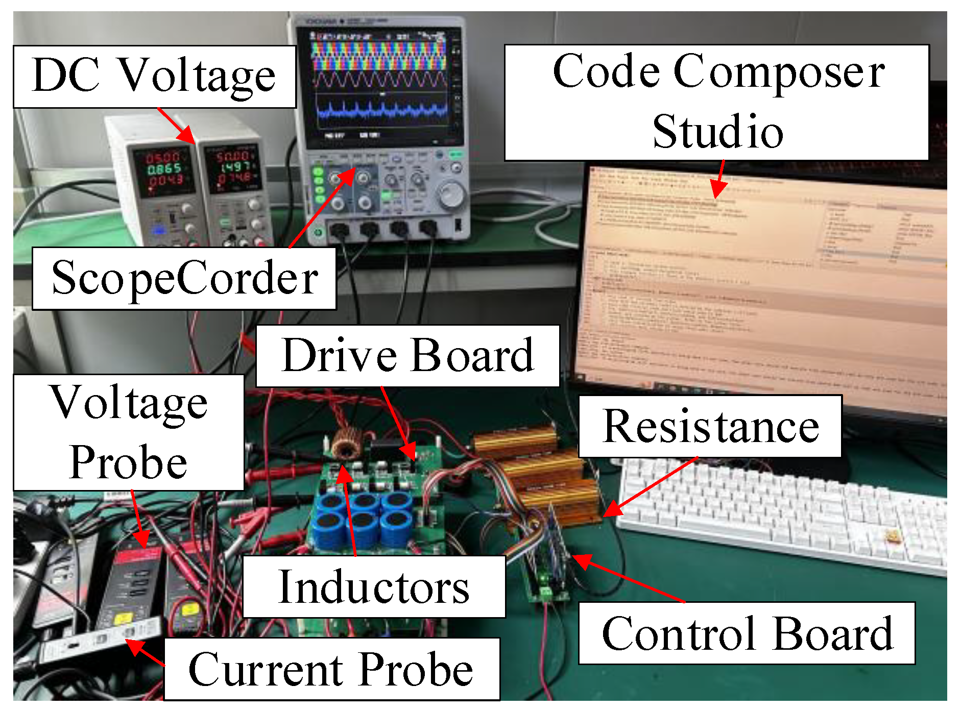
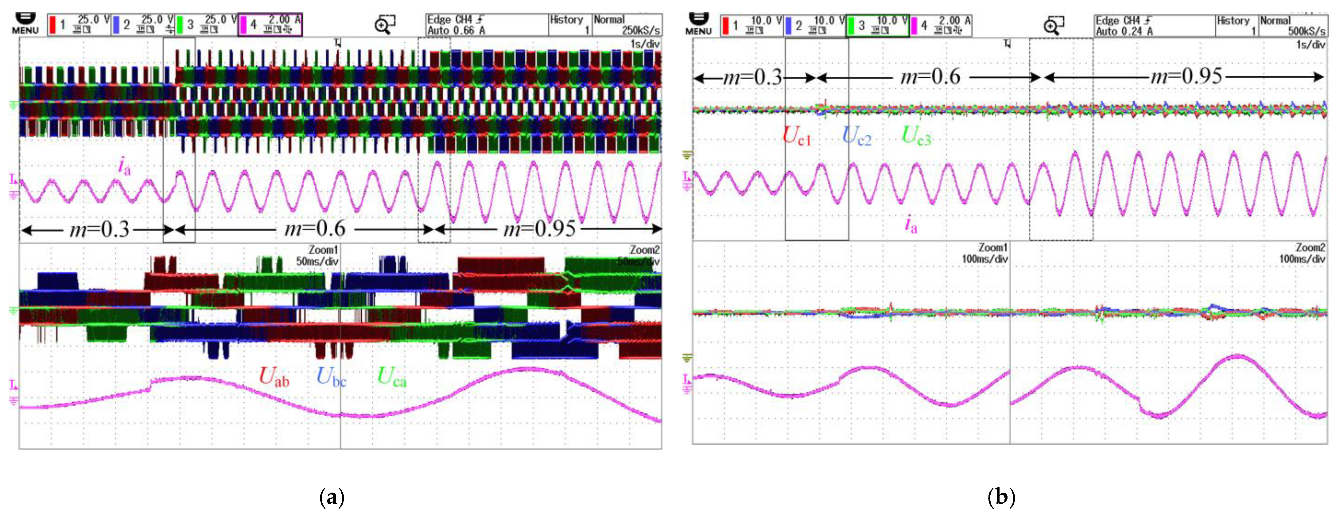
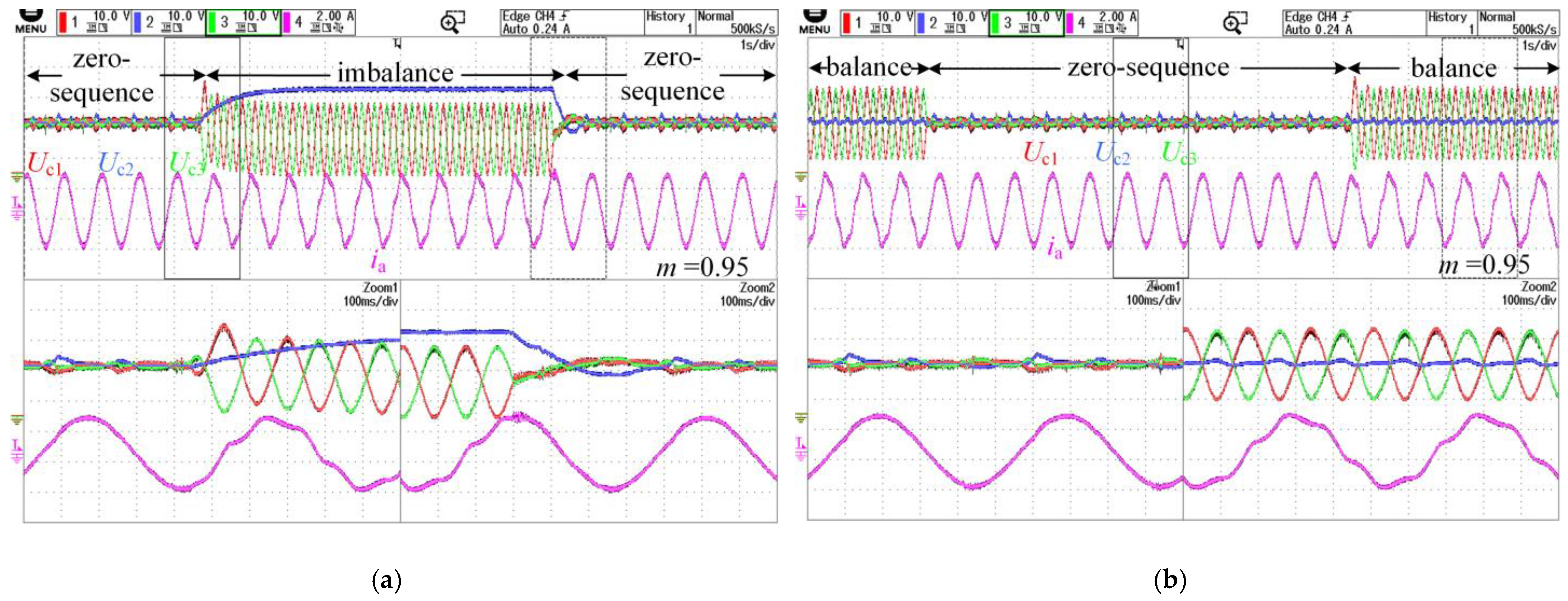
4. Verification of Experimental Results

To validate the theoretical analysis, an experimental prototype of the 4L-ANPC inverter has been constructed, shown in Figure 10. The experimental parameters are consistent with the simulation parameters. The proposed “variable reference + zero-sequence injection” method is implemented and validated using a digital chip TMS320F28379 from Texas Instruments (Dallas, TX, USA).
Figure 11 shows the measured three-phase line voltage, the phase current ia, and the DC-link capacitor voltages Uc1, Uc2, and Uc3 of the 4L-ANPC inverter. The results are obtained with the application of the “variable reference” method. Figure 11a shows that at a modulation index of 0.3, the line voltage exhibits only 5 levels with voltage fluctuations. As the modulation index increases to 0.6 and 0.95, the line voltage extends to 7 levels with voltage fluctuations. However, with higher modulation indices, the load current waveform becomes increasingly distorted, while the capacitor voltages Uc1 and Uc3 remain balanced. Figure 11b demonstrates that the amplitude of the upper and lower capacitor voltage ripple increases with the modulation index. When the modulation index is 0.95, the upper and lower capacitor voltage ripple is around 20 V, the load current distortion is serious. The FFT analysis of the load current is shown in Figure 12. Its harmonics are mainly distributed near the switching frequency, and the highest harmonic peak is −15.60 dBA.
Figure 13 shows the measured three-phase line voltage, phase current ia, and the capacitor voltages Uc1, Uc2, and Uc3 of the 4L-ANPC inverter. In this case, the 4L-ANPC inverter applies the “variable reference + zero-sequence injection” method. Compared to the variable reference method, Figure 13a shows that at a modulation index of 0.3, the line voltage exhibits still only 5 levels, but the voltage fluctuation disappears. Figure 13b shows that the amplitude of the capacitor voltage ripple increases only slightly with the modulation index. At a modulation index of 0.3, the DC capacitor voltage ripple is almost negligible. This demonstrates that the “variable reference + zero-sequence injection” method can suppress the low-frequency ripple of the capacitor voltage at any modulation index.
The FFT analysis of the load current is presented in Figure 14. When the load current maintains a standard sinusoidal waveform at a modulation index of 0.95, its harmonics are predominantly concentrated near the switching frequency, with the highest harmonic peak at −37.42 dBA. Additionally, compared to the “variable reference” method, the harmonic distribution is more uniform in Figure 14. The experimental results demonstrate that the “variable reference + zero-sequence injection” method is more effective in suppressing the low-frequency ripple in the capacitor voltage, thereby confirming the accuracy of the theoretical analysis.
To more intuitively assess the effectiveness of the “variable reference + zero-sequence injection” method in suppressing the low-frequency ripple of the capacitor voltage, a modulation index of 0.95 is used as an example. Relevant experimental data for each modulation method are compared and analyzed. Figure 15 presents the experimental results of capacitor voltages under different modulation methods. Figure 15a illustrates the transition from the conventional CBPWM method to the variable reference voltage balancing method, highlighting the change from unbalanced to balanced upper and lower capacitor voltages. Although the upper and lower capacitor voltages have been balanced at 1/3Udc, the ripple amplitude is still as high as 20 V, and the load current waveform is still heavily distorted. Figure 15b shows the experimental results of the 4L-ANPC inverter when switching from the conventional CBPWM method to the “variable reference + zero-sequence injection” method. The capacitor voltage ripples are less than 5 V, and the load current becomes a standard sinusoidal waveform.
Figure 16 displays the experimental results of the line voltage for various modulation methods. Figure 16a illustrates the transition from the conventional CBPWM method to the “variable reference + zero-sequence injection” method. In Figure 16a, the line voltage has only five levels, and there are obvious voltage fluctuations in the line voltage; whereas, the 4L-ANPC line voltage after the injection of the zero-sequence signal has seven levels, and the voltage fluctuations disappear because the low-frequency pulsations are suppressed. Figure 16b shows the transition from the “variable reference” method to the “variable reference + zero-sequence injection” method. Under the “variable reference” balancing method, the line voltage waveform has seven levels, and there are also significant voltage fluctuations in this waveform due to the large amplitude of the upper and lower capacitor voltages, which disappear after the injection of the zero-sequence signal. Figure 17 shows the experimental results of the capacitor voltages Uc1, Uc2, and Uc3 during two modulation methods. Figure 17a depicts the transition from the “variable reference + zero-sequence injection” method to the conventional CBPWM method, and then, back to the “variable reference + zero-sequence injection” method. Figure 17b illustrates the transition from the “variable reference” method to the “variable reference + zero-sequence injection” method, and then, back to the “variable reference” method. It can be found that the amplitude of the upper and lower capacitor voltages is too large under the “variable reference” balancing method. The experimental results indicate that the proposed “variable reference + zero-sequence injection” method effectively reduces load current distortion and suppresses the low-frequency ripple in the capacitor voltage of the 4L-ANPC inverter, regardless of the modulation method used.

5. Conclusions

In this paper, a straightforward zero-sequence injection method for the CBPWM of a 4L-ANPC inverter is proposed. The injected zero-sequence voltage is determined based on three reference voltage signals and the DC-link capacitor voltage. This method does not require predictive modeling or redundant switching to ascertain the zero-sequence voltage signal. Additionally, the paper elucidates the mechanism behind the upper and lower capacitor voltage imbalance in the four-level inverter and introduces the reference voltage balancing method employed. Furthermore, a theoretical analysis is conducted to explain how the “zero-sequence injection” method suppresses or eliminates the upper and lower capacitor voltage ripples. The method is combined with the variable reference voltage balancing control to achieve balanced upper and lower capacitor voltages and suppress their low-frequency voltage fluctuations as well. The experimental results of upper and lower capacitor voltages, phase currents, and line voltages across three methods—conventional CBPWM, “variable reference”, and “variable reference + zero-sequence injection”—are provided. These results demonstrate the effectiveness of the proposed method in mitigating low-frequency voltage fluctuations in the upper and lower capacitor voltages. Additionally, the suppression effect of the proposed method on the capacitor voltage ripple is compared across different modulation indices to verify the accuracy of the theoretical analysis.

Author Contributions

Validation, Y.W.; data curation, Z.H.; writing—original draft preparation, M.W.; writing—review and editing, J.C.; project administration, S.S. and Q.X.; All authors have read and agreed to the published version of the manuscript.

Funding

This research was funded by [National Natural Science Foundation of China] grant number [52207221] and [Natural Science Foundation of Hubei Province] grant number [2022CFB691].

Data Availability Statement

The datasets presented in this article are not readily available because the data are part of an ongoing study. Requests for access to the dataset should be made to the corresponding author.

Conflicts of Interest

Author Shi Su and Qingyang Xie was employed by the company Yunnan Power Grid Co., Ltd. The remaining authors declare that the research was conducted in the absence of any commercial or financial relationships that could be construed as a potential conflict of interest.

References

  1. Wang, J.; Yang, B.; Zhao, J.; Deng, Y.; He, X.; Zhixin, X. Development of a compact 750KVA three-phase NPC three-level universal inverter module with specifically designed busbar. In Proceedings of the 2010 Twenty-Fifth Annual IEEE Applied Power Electronics Conference and Exposition (APEC), Palm Springs, CA, USA, 21–25 February 2010; pp. 1266–1271. [Google Scholar]
  2. Hosoda, H.; Peak, S. Multi-level converters for large capacity motor drive. In Proceedings of the 2010 International Power Electronics Conference-ECCE ASIA-, Sapporo, Japan, 21–24 June 2010; pp. 516–522. [Google Scholar]
  3. Zhang, D.; He, J.; Pan, D. A megawatt-scale medium-voltage high-efficiency high power density “SiC + Si” hybrid three-level ANPC inverter for aircraft hybrid-electric propulsion systems. IEEE Trans. Ind. Appl. 2019, 55, 5971–5980. [Google Scholar] [CrossRef]
  4. Jiao, Y.; Lee, F.C. New modulation scheme for three-level active neutral-point-clamped converter with loss and stress reduction. IEEE Trans. Ind. Electron. 2015, 62, 5468–5479. [Google Scholar] [CrossRef]
  5. Li, C.; Lu, R.; Li, C. Space vector modulation for SiC and Si hybrid ANPC converter in medium-voltage high-speed drive system. IEEE Trans. Power Electron. 2019, 35, 3390–3401. [Google Scholar] [CrossRef]
  6. Wang, B. Four-level neutral point clamped converter with reduced switch count. In Proceedings of the 2008 IEEE Power Electronics Specialists Conference, Rhodes, Greece, 15–19 June 2008; pp. 2626–2632. [Google Scholar]
  7. Pribadi, J.; Lee, D.-C. Open-Switch Fault Diagnosis in Four-Level Active Neutral-Point-Clamped Inverters. In Proceedings of the 2021 IEEE Energy Conversion Congress and Exposition (ECCE), Vancouver, BC, Canada, 10–14 October 2021; pp. 2576–2581. [Google Scholar]
  8. Wang, K.; Zheng, Z.; Li, Y. Topology and control of a four-level ANPC inverter. IEEE Trans. Power Electron. 2022, 35, 2342–2352. [Google Scholar] [CrossRef]
  9. Chen, H.; He, Y.; Liu, J. A novel hybrid SVPWM modulation algorithm for five level active neutral-point-clamped converter. In Proceedings of the 2019 IEEE Applied Power Electronics Conference and Exposition (APEC), Anaheim, CA, USA, 17–21 March 2019; pp. 2494–2498. [Google Scholar]
  10. Wang, K.; Zheng, Z.; Li, Y. Neutral-point potential balancing of a five-level active neutral-point-clamped inverter. IEEE Trans. Ind. Electron. 2012, 60, 1907–1918. [Google Scholar] [CrossRef]
  11. Oikonomou, N.; Gutscher, C.; Karamanakos, P. Model predictive pulse pattern control for the five-level active neutral-point-clamped inverter. IEEE Trans. Ind. Appl. 2013, 49, 2583–2592. [Google Scholar] [CrossRef]
  12. Hachlowski, J.; Stala, R. DC-link voltage balancing converter with resonant switched-capacitor circuit for four-level and six-level NPC inverter. In Proceedings of the 2019 21st European Conference on Power Electronics and Applications (EPE’19 ECCE Europe), Genova, Italy, 3–5 September 2019; pp. 1–10. [Google Scholar]
  13. Busquets-Monge, S.; Bordonau, J.; Rocabert, J. A virtual-vector pulse width modulation for the four-level diode-clamped DC–AC converter. IEEE Trans. Power Electron. 2008, 23, 1964–1972. [Google Scholar] [CrossRef]
  14. Pham, K.D.; Phan, Q.D.; Nguyen, N.V. Novel virtual vector SVPWM method to mitigate low-frequency common mode voltage for four-level NPC inverters. IEEE Access 2024, 12, 22403–22419. [Google Scholar] [CrossRef]
  15. Yang, Y.; Pan, J.; Wen, H. An optimized model predictive control for three-phase four-level hybrid-clamped converters. IEEE Trans. Power Electron. 2019, 35, 6470–6481. [Google Scholar] [CrossRef]
  16. Monfared, K.K.; Iman-Eini, H.; Neyshabouri, Y. Model predictive control with reduced common-mode voltage based on optimal switching sequences for nested neutral point clamped inverter. IEEE Trans. Ind. Electron. 2023, 71, 27–38. [Google Scholar] [CrossRef]
  17. Wang, K.; Xu, L.; Zheng, Z. Capacitor voltage balancing of a five-level ANPC converter using phase-shifted PWM. IEEE Trans. Power Electron. 2014, 30, 1147–1156. [Google Scholar] [CrossRef]
  18. Wang, K.; Zheng, Z.; Xu, L. An optimized carrier-based PWM method and voltage balancing control for five-level ANPC converters. IEEE Trans. Ind. Electron. 2019, 67, 9120–9132. [Google Scholar] [CrossRef]
  19. Chen, J.; Wang, C. Dual T-type four-level converter. IEEE Trans. Power Electron. 2019, 35, 5594–5600. [Google Scholar] [CrossRef]
  20. Chen, J.; Zhong, Y.; Wang, C. Four-level hybrid neutral point clamped converters. IEEE J. Emer. Sel. Top. Power. Electron. 2021, 9, 4786–4801. [Google Scholar] [CrossRef]
  21. Li, C.; Chen, J. Simplified SVPWM capacitor voltage balancing control method for four-level neutral point clamped inverters. In Proceedings of the 2023 IEEE 14th International Symposium on Power Electronics for Distributed Generation Systems (PEDG), Shanghai, China, 9–12 June 2023; pp. 127–132. [Google Scholar]
  22. Wang, Y.; Chen, J. Voltage balancing control and implementation of detroit rectifier. IEEE Trans. Ind. Electron. 2024. [Google Scholar] [CrossRef]
  23. Wang, K.; Zheng, Z.; Li, Y. A novel carrier-overlapped PWM method for four-level neutral-point clamped converters. IEEE Trans. Power Electron. 2018, 34, 7–12. [Google Scholar] [CrossRef]
  24. Wang, K.; Zheng, Z.; Xu, L. A composite voltage-balancing method for four-level NPC inverters. IEEE J. Emer. Sel. Top. Power. Electron. 2020, 9, 3394–3406. [Google Scholar] [CrossRef]
  25. Wang, K.; Xu, L.; Zheng, Z. Multi-objective optimization control of a four-level hybrid-clamped inverter. In Proceedings of the 2015 IEEE Energy Conversion Congress and Exposition (ECCE), Montreal, QC, Canada, 20–24 September 2015; pp. 1611–1616. [Google Scholar]
  26. Qin, J.; Saeedifard, M. A zero-sequence voltage injection-based control strategy for a parallel hybrid modular multilevel HVDC converter system. IEEE Trans. Power Deliv. 2014, 30, 728–736. [Google Scholar] [CrossRef]
  27. Wang, K.; Xu, L.; Zheng, Z. Voltage balancing control of a four-level hybrid-clamped converter based on zero-sequence voltage injection using phase-shifted PWM. IEEE Trans. Power Electron. 2015, 31, 5389–5399. [Google Scholar] [CrossRef]
  28. Pou, J.; Zaragoza, J.; Rodríguez, P. Fast-processing modulation strategy for the neutral-point-clamped converter with total elimination of low-frequency voltage oscillations in the neutral point. IEEE Trans. Ind. Electron. 2007, 54, 2288–2294. [Google Scholar] [CrossRef]
  29. Chen, J. A new insight on four-level neutral point clamped converters: Four-level = two-level + three-level. IEEE Trans. Power Electron. 2024, 39, 5166–5177. [Google Scholar] [CrossRef]
Figure 1. The topology of the 4L-ANPC inverter.
Electronics 13 03878 g001
Figure 2. Variable reference method control diagram.
Electronics 13 03878 g002
Figure 3. The structure of the adopted “variable reference + zero-sequence injection” method.
Electronics 13 03878 g003
Figure 4. A duty cycle of different output levels in one switching cycle. (a) Positive fundamental period; (b) negative fundamental period.
Electronics 13 03878 g004
Figure 5. The modulating waveform of the variable reference voltage balancing method.
Electronics 13 03878 g005
Figure 6. Simulation results of intermediate capacitor voltage with different modulation methods. (a) “Variable reference” method; (b) “variable reference + zero-sequence injection” method.
Electronics 13 03878 g006
Figure 7. Simulation results of upper and lower capacitor voltage with different modulation methods. (a) “variable reference” method; (b) “variable reference + zero-sequence injection” method.
Electronics 13 03878 g007
Figure 8. Simulation results of phase current with different modulation methods. (a) “Variable reference” method; (b) “variable reference + zero-sequence injection” method.
Electronics 13 03878 g008
Figure 9. Simulation results of phase current FFT with different modulation methods. (a) “Variable reference” method; (b) “variable reference + zero-sequence injection” method.
Electronics 13 03878 g009
Figure 10. The 4L-ANPC inverter experimental prototype.
Electronics 13 03878 g010
Figure 11. Experimental results of “variable reference” method. (a) Three-phase line voltage; (b) capacitor voltages Uc1, Uc2, Uc3.
Electronics 13 03878 g011
Figure 12. Load current FFT analysis for the “variable reference” method.
Electronics 13 03878 g012
Figure 13. Experimental results of “variable reference + zero-sequence injection” method. (a) Three-phase line voltage; (b) capacitor voltages Uc1, Uc2, Uc3.
Electronics 13 03878 g013
Figure 14. Load current FFT analysis for “variable reference + zero-sequence injection” method.
Electronics 13 03878 g014
Figure 15. Experimental results of capacitor voltages under different modulation methods. (a) Conventional CBPWM method to the “variable reference” method; (b) conventional CBPWM method to the “variable reference + zero-sequence injection” method.
Electronics 13 03878 g015
Figure 16. Experimental results of line voltages for different modulation methods. (a) Conventional CBPWM method to “variable reference + zero-sequence injection” method; (b) “variable reference” method to “variable reference + zero-sequence injection” method.
Electronics 13 03878 g016
Figure 17. Experimental results of capacitor voltage during two switching modulation methods. (a) Secondary switching between “variable reference + zero-sequence injection” and conventional CBPWM method; (b) secondary switching between “variable reference + zero-sequence injection” and “variable reference” method.
Electronics 13 03878 g017
Table 1. Simulation parameter.
ParameterValue
DC-link voltage Udc50 V
DC-link capacitors1.32 mF
Switching frequency fs10 kHz
LR Load5 mH, 10 Ω
Fundamental current2 Hz
Disclaimer/Publisher’s Note: The statements, opinions and data contained in all publications are solely those of the individual author(s) and contributor(s) and not of MDPI and/or the editor(s). MDPI and/or the editor(s) disclaim responsibility for any injury to people or property resulting from any ideas, methods, instructions or products referred to in the content.

