Review

Diamond FET Biosensor Fabrication and Application

1
School of Electro-Mechanical Engineering, Guangdong University of Technology, Guangzhou 510006, China
2
Guangdong Provincial Key Laboratory of Minimally Invasive Surgical Instruments and Manufacturing Technology, Guangdong University of Technology, Guangzhou 510006, China
3
State Key Laboratory for High Performance Tools, Guangdong University of Technology, Guangzhou 510006, China
4
Smart Medical Innovation Technology Center, Guangdong University of Technology, Guangzhou 510006, China
*
Author to whom correspondence should be addressed.
Electronics 2024, 13(19), 3881; https://doi.org/10.3390/electronics13193881
Submission received: 23 August 2024 / Revised: 26 September 2024 / Accepted: 28 September 2024 / Published: 30 September 2024
(This article belongs to the Section Bioelectronics)

Abstract

:
Diamond is renowned as the ultimate semiconductor thanks to its exceptional physical properties, including unmatched hardness, exceptional wear resistance, superior mechanical and tribological characteristics, and high fracture strength. Diamond solution-gate field-effect transistors (D-SGFETs) leverage these advantages, along with their outstanding high-power and high-frequency performance, excellent thermal conductivity, wide bandgap, high carrier mobility, and rapid saturation speed. These features make D-SGFETs highly promising for fast and precise biomedical detection applications. This paper provides a comprehensive review of the fabrication techniques for diamond SGFETs, encompassing diamond film synthesis, surface conduction layer formation, source/drain fabrication, and FET packaging. Furthermore, the study delves into the surface functionalization of diamond SGFETs and their diverse applications in biomedical detection. Finally, the paper discusses the future outlook of diamond SGFETs in advancing biomedical detection technologies.

1. Background

Carbon-based semiconductors such as graphene [1], carbon nanotubes [2], carbon nanowires [3,4,5], carbon nanofibers [6], carbon nanospheres [6,7], and diamond [8] exhibit high specific surface area, excellent electrical conductivity, chemical stability, biocompatibility, and robust mechanical strength [9]. These properties have attracted considerable attention in the field of biomedical detection [10]. Among these materials, diamond stands out due to its exceptional attributes, including unparalleled hardness, superior wear and corrosion resistance, wide electrochemical potential window, high thermal conductivity, wide bandgap, high critical breakdown field strength, and outstanding biocompatibility. Diamond has been utilized in various biomedical assays, such as antibody–antigen interactions [11] and DNA hybridization [12,13].
Diamond, an allotrope of carbon, consists of a network where each carbon atom forms stable covalent bonds with four other carbon atoms in a tetrahedral hybridized structure. This configuration makes diamond one of the hardest materials on Earth, endowed with exceptional wear and corrosion resistance [14]. Diamond also features a large electrochemical potential window and high chemical stability, with a thermal conductivity of up to 2400   W / m · K [8], which is four times that of silicon carbide. In addition to these attributes, diamond is a novel wide bandgap material, with a bandgap of approximately 5.5   eV [8]. It has an inert surface and a critical breakdown field strength of up to 10   MV / cm [8]. Its excellent insulating properties are maintained at room temperature, with a resistivity of approximately 10 16   Ω · cm [15]. The insulating nature of diamond can be modified by doping it with metal atoms to create P-type or N-type semiconductors. Alternatively, a P-type hole conductive layer can be formed by hydrogen termination on the diamond surface, achieving a hole surface density of up to 10 13 / cm 2 [16]. Diamond also boasts higher electron and hole mobility compared to other wide-bandgap semiconductors at room temperature, with electron mobility around 4500   cm 2 / V · s and hole mobility around 3300   cm 2 / V · s [17]. It exhibits exceptionally high saturation velocities, with electron saturation velocity approximately 2 × 10 7 cm / s and hole saturation velocity around 1.2 × 10 7 cm / s [18]. Moreover, diamond has excellent biochemical properties and biocompatibility [19,20]. Various functional groups, such as halogens [21,22], amino groups [23,24,25,26], and oxygen-containing groups (carbonyl, carboxyl) [27,28,29,30], can be introduced onto the diamond surface through chemical modification. This allows for precise control over the surface properties, such as wettability [31,32,33,34] and biocompatibility [32]. Given its exceptional mechanical, physical, and biochemical properties, diamond is an ideal material for the fabrication of biosensors and holds significant promise for applications in biomedical detection [35,36].
In biosensors, converting biometric responses into measurable signals, such as electrical or optical outputs, has always been a significant challenge. Solution-gate field-effect transistors (SGFETs) offer an effective solution to this problem due to their high input resistance [37], low noise [37], high sensitivity [38], low power consumption, wide dynamic range, ease of integration, absence of secondary breakdown, broad safe operating area, and capability for real-time monitoring. These features make SGFETs ideal devices for signal conversion and amplification in biosensors, significantly improving the speed and convenience of biomedical detection [1]. Currently, SGFETs come in various types depending on their structure, materials, and applications, and they can be broadly categorized as follows: Silicon-based SGFET (Si-SGFET), Oxide-based SGFET (O-SGFET), Graphene SGFET (G-SGFET), Gallium Nitride SGFET (GaN-SGFET), and Diamond SGFET (D-SGFET). Traditional SGFETs primarily use silicon as the semiconductor material. Table 1 summarizes the material properties and figures of merit (normalized to Si = 1) at room temperature for diamond and silicon. Silicon has a relatively narrow bandgap of approximately 1.1   eV [39], which limits its performance under high-temperature and high-pressure conditions, making it less suitable for extreme environments and demanding biosensing applications. Silicon’s thermal conductivity is around 150   W / m · K [40], its electron mobility is approximately 1400   cm 2 / V · s [41], and its hole mobility is about 450   cm 2 / V · s   [41]. The electron and hole saturation velocities are roughly 1 × 10 7 cm / s and 6 × 10 6 cm / s [18], respectively. While silicon’s hole saturation speed is relatively high, its overall electronic properties are lower than those of diamond. Diamond, on the other hand, exhibits an extremely high electron saturation velocity and superior thermal conductivity. Moreover, diamond has exceptional biocompatibility compared to silicon, which tends to oxidize in liquid environments, forming silicon oxide. This oxidation can reduce silicon’s functionalization potential, corrosion resistance, and durability, which may lead to stability issues in biological applications. In contrast, the quality factor of diamond highlights its superior electronic properties over silicon [8]. Compared to Si-SGFETs, D-SGFETs are better suited for complex biomedical detection environments due to their outstanding attributes, such as high power handling [42], high-frequency performance, excellent thermal conductivity [8], wide bandgap [8], high carrier mobility [17], and fast saturation velocity [8]. These characteristics make D-SGFETs more effective than other types of SGFETs for complex biomedical applications.
In 1989, Shiomi et al. [17] produced the first diamond metal-semiconductor field-effect transistor (D-MESFET) using boron-doped epitaxial diamond films. In 2001, H. Kawarada et al. [1] developed a diamond solution-gate field-effect transistor (D-SGFET) based on hydrogen-terminated diamond surfaces, capitalizing on the pH insensitivity of these surfaces. They proposed that an ion-selective region could be created on the hydrogen-terminated diamond surface to form a biosensor using D-SGFETs. Since then, D-SGFETs have become integral to biosensing applications, and over 20 years of research have led to their widespread adoption in biomedical detection. In the realm of biomedical detection, the ability to accurately detect biomolecules is essential for disease diagnosis and monitoring, drug development, biological research, and personalized medicine. D-SGFETs have proven capable of detecting various biomolecules, with common detection methods based on diamond FETs including ion detection [43,44,45], protein detection [27,30,46,47,48], nucleic acid detection [13,26,28,49,50,51], urea detection [24,51], glucose detection [51,52], and water content detection [53]. In D-SGFETs, charged biomolecules precisely modulate carrier concentration through the highly sensitive electric double layer (EDL) formed at the diamond surface–solution interface, which in turn regulates the detection current.
This paper begins by tracing the development of diamond FETs over the past 30 years, emphasizing key advancements in their fabrication. It then explores the core manufacturing processes of D-SGFETs and their applications in biomedical detection. Finally, the paper reviews the current state of diamond SGFETs and offers insights into their future development potential.

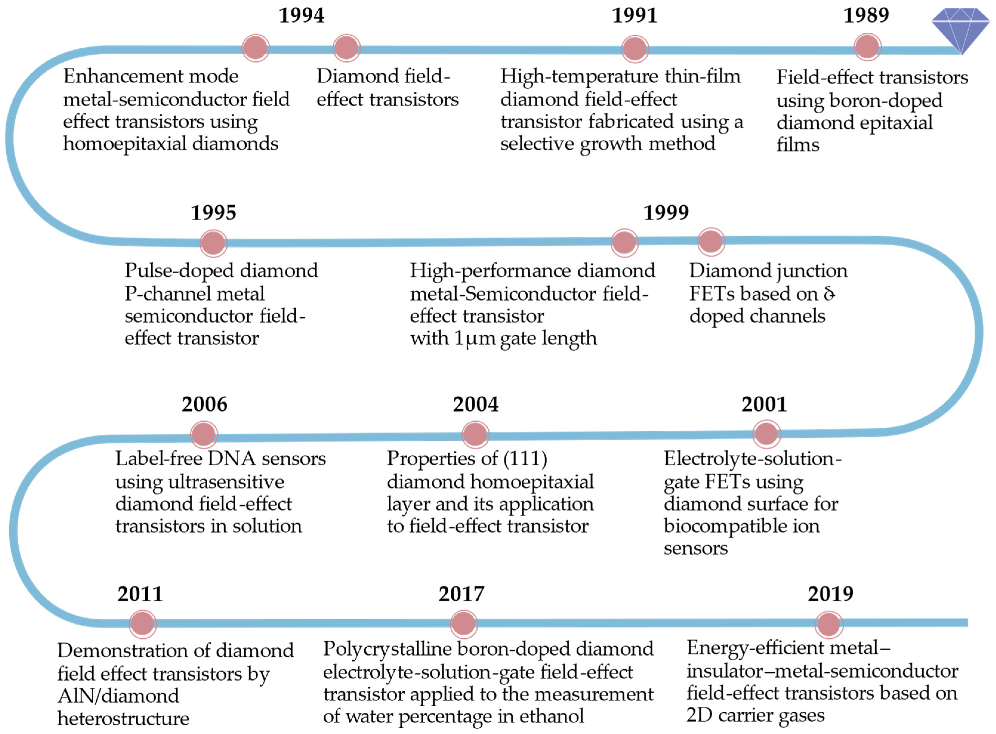
2. Development History of Diamond FET

Diamond FETs can be broadly classified into two categories based on the gate materials: solid-gate FETs and solution-gate FETs. Figure 1 provides optical micrographs of diamond FETs featuring different gate materials. Solid-gate diamond FETs are further subdivided into Diamond Metal–Semiconductor Field-Effect Transistors (D-MESFETs), Diamond Metal–Insulator-Semiconductor Field-Effect Transistors (D-MISFETs), and Diamond Metal–Oxide-Semiconductor Field-Effect Transistors (D-MOSFETs). These classifications depend on the presence and type of gate dielectric layer. In contrast, the gate of a diamond solution-gate FET is immersed in a liquid environment, typically referred to as Diamond Solution-Gate Field-Effect Transistors (D-SGFETs) or Diamond Ion-Sensitive Field-Effect Transistors (D-ISFETs).
Figure 2 illustrates schematic diagrams of various types of diamond FETs. D-MESFETs lack a gate dielectric layer, where the gate forms a Schottky junction directly with the diamond semiconductor. D-MISFETs, on the other hand, introduce a thin insulating layer between the gate and the diamond, enhancing gate voltage control and improving device stability. Similarly, D-MOSFETs utilize an oxide layer as the insulating layer, offering better gate control but facing challenges in liquid environments, which can damage or destabilize the oxide, limiting its application in biosensing. Unlike these solid-gate FETs, D-SGFETs forgo a conventional dielectric layer altogether. Instead, the liquid electrolyte serves as the gate, modulating the gate potential through ions or biomolecules present in the solution. The absence of a solid dielectric layer makes D-SGFETs particularly sensitive to ion concentration fluctuations, enabling the detection of a wide range of biomolecules and complex biological processes. This sensitivity renders D-SGFETs ideal for biomedical applications.
Figure 3 presents a roadmap of the development of diamond FETs, highlighting significant breakthroughs. This section focuses on the development history of D-SGFETs.
In 1989, Hiromu Shiomi et al. [42] used plasma chemical vapor deposition to produce boron-doped diamond epitaxial films and successfully created the first D-MESFETs, observing the basic operation of diamond FETs, characterized by distinct I–V characteristics. In 1991, Gennady Sh. Gildenblat et al. [56] fabricated the first D-MISFET on boron-doped homogeneous epitaxial monocrystalline diamond films. In 1994, David L. Dreifus et al. [57] constructed the first D-MOSFET on boron-doped single-crystal diamond.
In 2001, H. Kawarada et al. [1] successfully fabricated a D-SGFET on hydrogen-terminated diamond. They achieved excellent pinch-off and saturation I-V characteristics within the bias voltage window and proposed that D-SGFETs could serve as a basis for biosensors, owing to the pH insensitivity of H-terminated diamond surfaces. The surface properties of diamond differ significantly between hydrogen-terminated (H-terminated) and oxygen-terminated (O-terminated) surfaces. H-terminated diamond exhibits p-type surface conductivity even without doping, whereas O-terminated diamond is insulating. Toshikatsu Sakai et al. [58] fabricated partially O-terminated D-SGFETs through ozone treatment. They observed that, although the channel region became partially O-terminated and highly resistive after O 3 treatment, the device could still operate stably. The O 3 treatment shifted the device’s threshold voltage in the negative direction and enhanced its sensitivity to positive ions or neutral molecules without interference from negative ions. Jose A. Garrido et al. [59] discovered that while H-terminated D-ISFETs were insensitive to pH changes, surfaces modified through oxygen bonding after O 3 treatment exhibited significant pH sensitivity. Charges adsorbed in the O-terminated sensitive region could modulate the conductivity of the adjacent H-terminated conduction channels via electrostatic interactions. Thus, the oxidized region acts as a lateral, chemically sensitive gate, allowing for super-Nernstian pH sensitivity (>59 mV/pH).
In 2007, A. Denisenko et al. [60] developed the first boron δ-doped diamond pH-sensitive ISFET, achieving near-Nernstian pH sensitivity ( 59   mV / pH ) by employing wet chemical oxidation of the diamond surface. This device combined a chemically stable FET channel with a surface well-suited for reliable pH sensing. In the same year, B. Rezek et al. [61] fabricated pH-sensitive D-ISFETs using H-terminated diamond films, demonstrating a pH response of approximately 56   mV / pH without the need for surface oxidation. Despite these advancements, the miniaturization of D-SGFETs to the micron or submicron scale, as achieved with silicon-based ion-sensitive FETs, remains a challenge. However, scaling down the gate length and width by a factor of 1 / k reduces the chip size by 1 / k 2 and decreases the required sample volume for biomedical detection by 1 / k 3 . In short-channel FETs, the sensitivity to gate potential shifts caused by specific reactions remains unchanged, but higher transconductance ( g m ) and greater overall sensitivity are achieved. Song, Kwang-Sou et al. [24] utilized electron beam lithography to miniaturize the channel length in D-SGFETs to 50   nm , achieving a width of 300   nm and a high transconductance of 33   mS / mm , which is 930 times greater than that of a D-SGFET with a longer channel length of 500   μ m ( 60   μ S / mm ). The urea sensor fabricated with this D-SGFET exhibited an impressive sensitivity of 27   μ A / decade . Although packaging devices using electron beam lithography for lithographic layers can be complex, Shaili Falina et al. [62] demonstrated that using titanium oxide ( TiO X ) as a source/drain metal contact package for D-SGFETs is a feasible alternative. These TiO X -packaged D-SGFETs exhibited excellent SGFET performance, especially in short-gate-length devices ( L G = 5   μ m ), with a very high maximum current density of 800   mA / mm and excellent transconductance. The devices also demonstrated reliable responses over a wide pH range ( 2 ~ 12 ).
A. Denisenko et al.’s boron δ-doped D-SGFETs were fabricated on (100)-oriented diamond, while boron δ-doping layers grown on (111)-oriented diamond could offer additional advantages. The boron doping density is eight times higher on (111) planes compared to (100) planes, allowing for a higher doping concentration at lower film thicknesses. The migration rate of boron atoms in δ-doped (111) diamond layers is also stronger, leading to an almost ideal sheet carrier density. After oxidation, the hydroxyl group density on (111)-oriented diamond is higher than on (100)-oriented diamond, enhancing pH sensitivity. Robert Edgington et al. [63] were the first to fabricate an SGFET with an oxidized boron δ-doped channel on (111) diamond. Compared to similar devices based on (100)-oriented diamond, this device exhibited better I–V characteristics, achieving a maximum gain of three and a transconductance of 200   μ S / mm . It also demonstrated moderate pH sensitivity of 36   mV / pH and a rapid response to pH changes, comparable to oxygen-terminated D-SGFETs. In addition to using glass electrodes, reference electrodes, or quasi-reference electrodes as gates in D-SGFETs, stainless steel containers can also serve as gates. Shuto Kawaguchi et al. [64] utilized a pH-sensitive stainless steel container in combination with a partially O-terminated D-SGFET, which is insensitive to pH, to achieve a highly sensitive pH system ( 54.6   mV / pH ) at 95   ° C .
Beyond the MES, MIS, MOS, and solution-gate structures, researchers have developed various other structures for diamond FETs. These include diamond junction field-effect transistors (JFETs) [65,66], diamond heterojunction field-effect transistors (HFETs) [67], diamond metal-insulator-metal-semiconductor field-effect transistors (MIMS-FETs) [68], and diamond multigate field-effect transistors [69].
Diamond FETs, as a cutting-edge semiconductor technology, have undergone over 30 years of research and development, demonstrating remarkable characteristics and potential across various applications.

3. Diamond SGFET

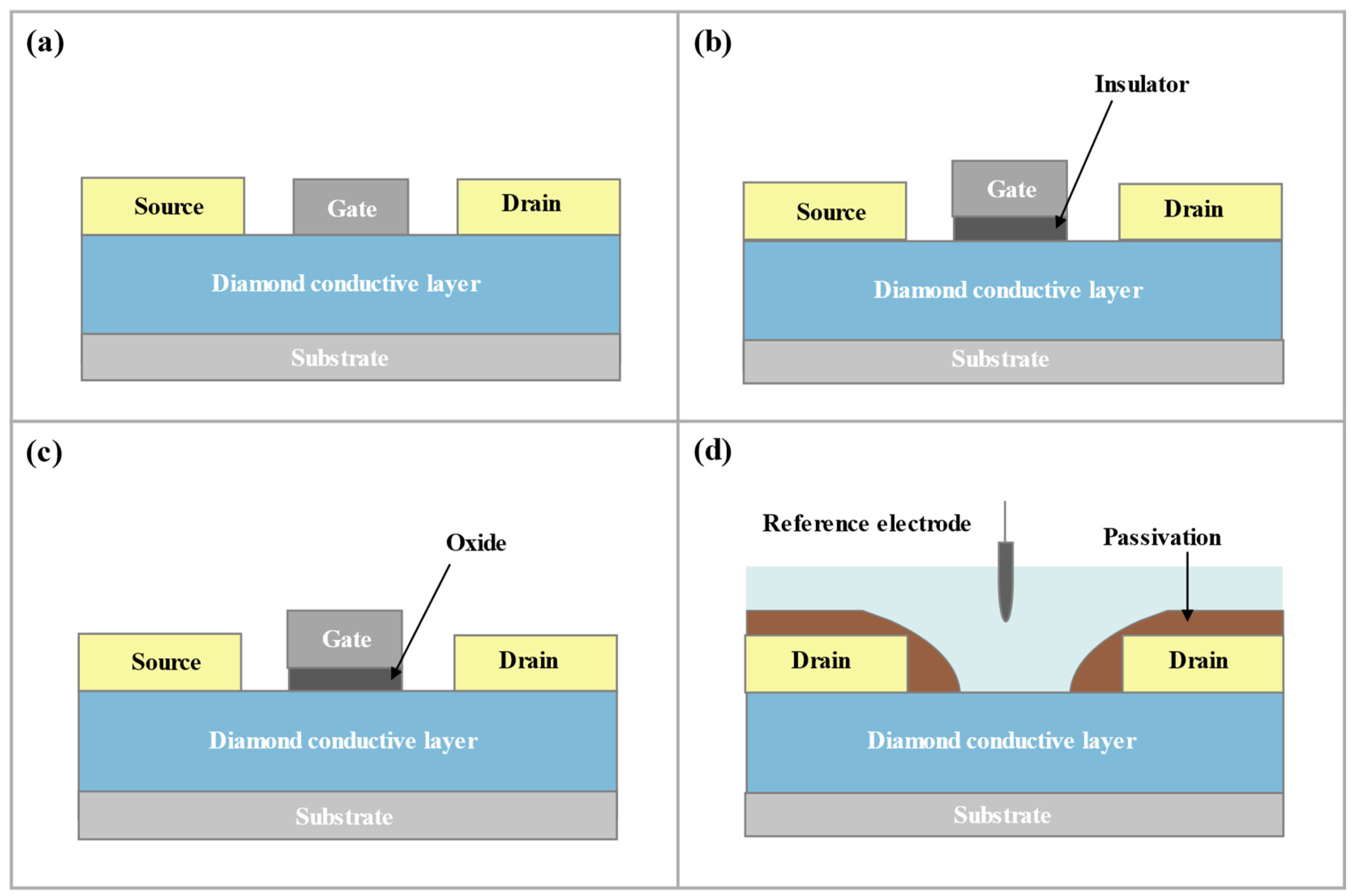
3.1. Introduction of D-SGFET

The working principle of D-SGFETs is based on the formation of an electric double layer (EDL) at the interface between the diamond surface and the electrolyte solution. The EDL consists of two layers: a tightly bound ion layer that adheres directly to the diamond surface and a more diffuse layer located further away in the electrolyte. This structure behaves like a capacitor, known as “EDL capacitance”. Due to the nanometer-scale thickness of the EDL, its capacitance is exceptionally high, making D-SGFETs highly sensitive to changes in surface potential, which are influenced by ions or biomolecules in the solution. When specific charged biomolecules bind to the functionalized diamond surface, they alter the local surface charge, thereby modulating the EDL capacitance. This, in turn, affects the carrier concentration in the diamond’s conductive channel, and the change is detected through variations in current or gate voltage [48]. This high sensitivity allows D-SGFETs to be effective for biosensing applications. Moreover, D-SGFETs offer excellent chemical resistance and biocompatibility, enabling stable interfaces with biomolecules, including covalent bonding [48,63]. They also provide a favorable signal-to-noise ratio and reliable signal stability [1,13]. As a result, D-SGFETs are well-suited for the direct detection of ions or biomolecules in solutions, making them ideal for biomedical applications. The following sections explore the application of D-SGFETs in biomedical sensing.

3.2. D-SGFET Fabrication Process

D-SGFETs are typically manufactured using a “bottom-up” process. First, a diamond film of the desired thickness is grown on a pre-cleaned substrate using techniques such as Chemical Vapor Deposition (CVD), Microwave Plasma Chemical Vapor Deposition (MPCVD), Hot Filament Chemical Vapor Deposition (HFCVD), Radio Frequency Plasma Enhanced Chemical Vapor Deposition (RF-PECVD), or High-Temperature High-Pressure (HPHT) methods. Afterward, metal doping or hydrogen surface treatment is applied to the diamond, imparting conductive properties to the surface layer. Next, the source and drain electrodes are fabricated through a combination of metal deposition, lithography, and etching processes. Finally, the D-SGFET is packaged as a detection device, with the exposed diamond surface serving as the sensing area. The size of this area is determined by the fabrication and packaging of the source and drain electrodes. The following sections detail the D-SGFET fabrication process according to these four key steps.

3.2.1. Diamond Film Synthesis

The diamond used in D-SGFET fabrication is typically synthetic diamond, which has the same structure and similar performance as natural diamond. However, the production process of synthetic diamonds can be precisely controlled, leading to lower costs and the potential for large-scale production, making them highly suitable for diamond FET fabrication.
The synthesis of diamond films on a substrate involves two main steps: substrate pretreatment and film growth. Substrate pretreatment generally includes cleaning and adjusting the surface roughness. Surface roughness is achieved through etching or specific surface treatments, enhancing the bonding strength between the diamond film and the substrate. For non-diamond substrates, an additional step—diamond nucleation—is necessary before film growth. Diamond nucleation sites are crucial for the successful epitaxial growth of diamond on such substrates, with bias-enhanced nucleation being the most commonly used method [70]. Diamond films are synthesized using various techniques, including Chemical Vapor Deposition (CVD) [71] and High-Pressure High-Temperature (HPHT) methods [72], though CVD is the primary method.
CVD deposits a solid film on the substrate surface by reacting precursor gases, such as methane ( CH 4 ) and hydrogen ( H 2 ). The CVD process allows for precise control over reaction conditions, directly influencing the quality and performance of the diamond film. Varying deposition times lead to different diamond grain sizes, and CVD has minimal substrate size restrictions, enabling the synthesis of large-area single-crystal diamonds. Moreover, high-quality diamond films can be produced without introducing catalysts or impurities. CVD methods include MPCVD [71], HFCVD [73], RF-PECVD [74], among others, with MPCVD being the most widely used technique in D-SGFET manufacturing [50,58].

3.2.2. Diamond Semiconductor Manufacturing

Undoped pure diamond exhibits exceptional insulating properties, with a resistivity of approximately ρ > 10 15   Ω · cm . Currently, there are two primary methods for manufacturing diamond-based insulators: doping specific regions of the diamond or applying hydrogen treatment directly to the diamond surface. Figure 4 illustrates a schematic diagram of both boron-doped and H-terminated D-SGFETs.
The main methods for doping diamond include incorporation during CVD growth [64] and ion implantation [75]. Doping during CVD growth ensures uniformity with minimal defect introduction, while ion implantation offers precise control over the concentration of doped atoms and selective doping in specific areas. A common challenge for both P-type and N-type doping is achieving high mobility while increasing carrier concentration to enhance conductivity. Phosphorus and nitrogen are the most common N-type dopants [76,77], with activation energies at room temperature of 1.5   eV and 0.57   eV , respectively. These high activation energies can limit effective ionization at room temperature, resulting in lower carrier concentrations, which has led to limited study of N-type doped D-SGFETs. In contrast, boron doping [64] for P-type diamond, with its lower activation energy of 0.37   eV , improves both carrier mobility and overall device performance. Adjusting boron doping concentrations through sources such as trimethylboron [71] and diborane [78] is essential for enhancing the performance of boron-doped diamond. Additionally, boron atomic layer doping, or boron δ-doping, can be employed. This method involves introducing boron atoms into a thin layer (typically 1–2 nm in thickness), providing highly uniform and precise doping. Boron δ-doping helps mitigate local concentration heterogeneities and minimizes defects, leading to enhanced carrier mobility and improved electrical conductivity in the diamond [79,80].
Hydrogen treatment as an alternative to doping offers simplicity in its application. The principle involves exposing the diamond surface to hydrogen plasma, followed by air exposure. During this process, the C H bonds on the diamond surface interact with polar molecules such as water and carbon dioxide ( CO 2 ) in the near-surface adsorption layer, resulting in the formation of a two-dimensional hole gas (2DHG) conductive layer through electron transfer. The hole concentration and mobility achieved through hydrogen treatment can reach up to 10 13   cm 2 / V · s   [16] and 5 ~ 300   cm 2 / V · s   , respectively. Notably, when boron doping is performed in a hydrogen atmosphere during CVD, the surface of the boron-doped diamond can also form an H-terminated structure.

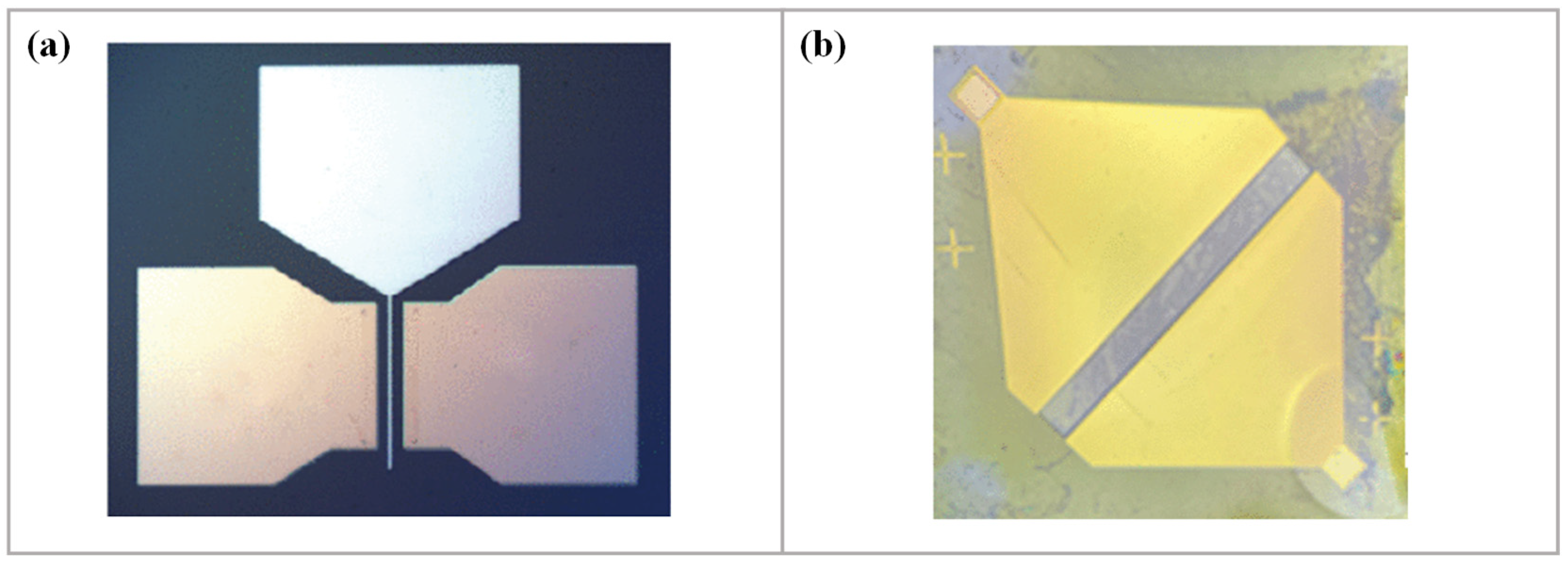
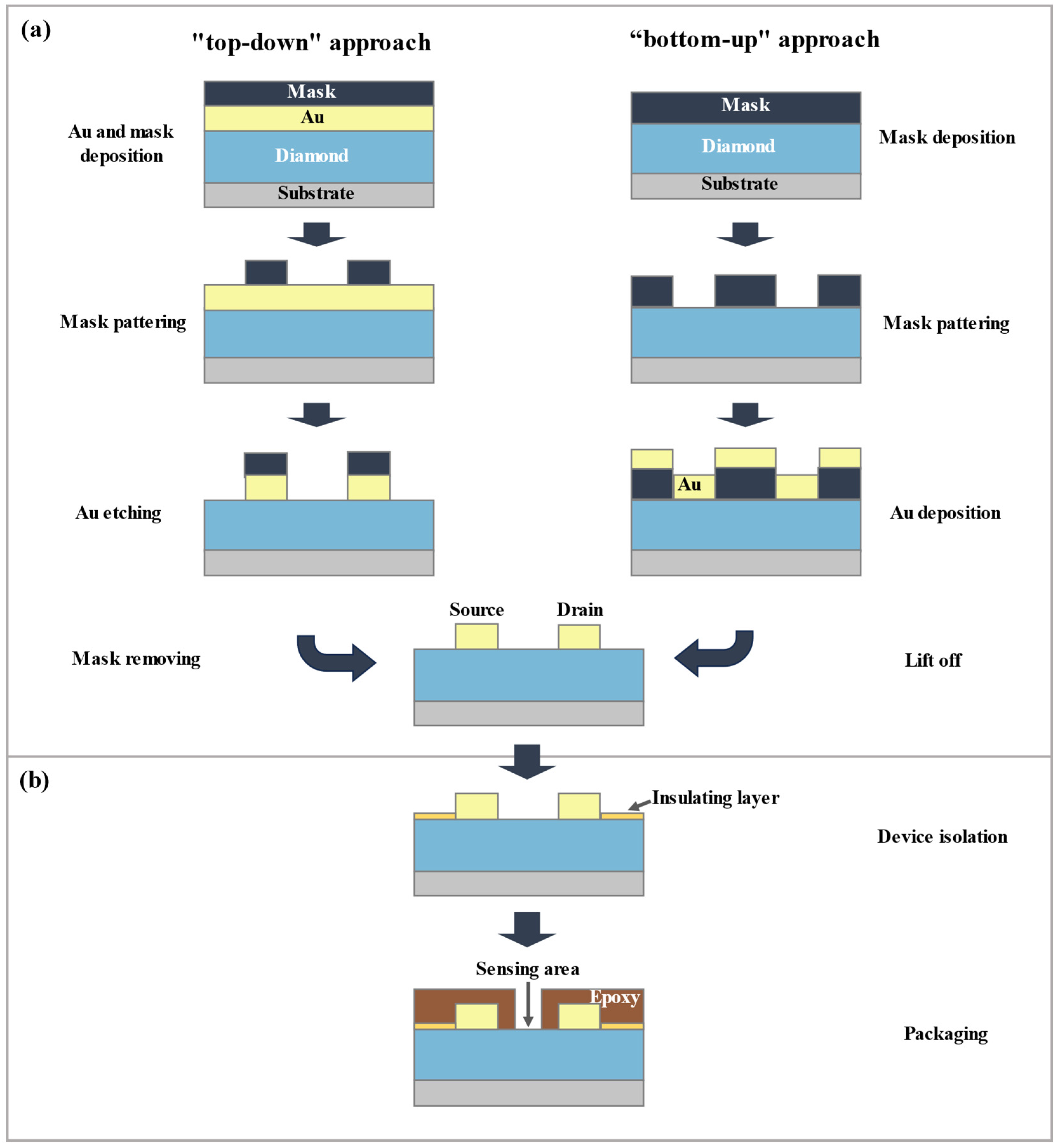
3.2.3. D-SGFET Source/Drain Fabrication

The source/drain fabrication of D-SGFETs involves establishing a reliable ohmic contact between the source/drain metal and the conductive layer on the diamond surface. This process can generally be divided into two primary approaches: the “top-down” and “bottom-up” methods, as illustrated in Figure 5a. In the top-down approach, metal electrode materials such as gold are deposited using techniques like electron beam deposition [64] or thermal evaporation [48]. These metals are then patterned using masking materials and etched to define the source/drain regions. Conversely, the bottom-up approach also uses masking techniques, but it involves the deposition and subsequent stripping of metal electrode materials to create the source/drain regions.
Gold is commonly used as the metal electrode material due to its strong adhesion to diamond. A titanium adhesive layer is often applied to reduce contact resistance and ensure optimal ohmic characteristics after annealing. Etching technologies play a crucial role in defining the intricate geometries of these regions. Reactive ion etching (RIE) [71], electron beam etching [81], and focused ion beam (FIB) etching [82] are commonly used techniques. RIE utilizes plasma bombardment to induce chemical reactions, while electron beam and FIB etching provide higher resolution through precise control of energy and dose, making them suitable for various materials.

3.2.4. D-SGFET Packaging

During the detection process, if the source/drain of a D-SGFET is exposed to the detection solution, it may short-circuit, potentially damaging the entire FET circuit. Additionally, if the conductive diamond surface outside the sensing area and the source/drain contact the detection solution, ions from the solution could penetrate the D-SGFET circuit, negatively affecting device performance. Therefore, the packaging of D-SGFETs is crucial for protecting and isolating critical components, ensuring electrical connectivity, enhancing stability and long-term performance, and facilitating integration and application. The packaging area is determined by how the source/drain connects to the circuit: if connected via bonding wires, the entire device, except the sensing area, should be packaged; if connected directly with probes, only the sensing area remains exposed. D-SGFET packaging generally involves two main steps. Figure 5b illustrates the packaging flowcharts for D-SGFET. The first step is to create a mask that isolates areas of the device other than the sensing area and the source/drain. Common methods include using ultraviolet (UV) irradiation in an O 3 or O 2 environment to form an oxygen-terminated layer [70] or injecting argon ions through a mask to create an insulating region [48].
The second step is the actual packaging of the device. A commonly used packaging material is insulating epoxy resin [64], valued for its affordability and straightforward packaging process. In addition to epoxy, researchers have explored the use of TiO X as an alternative material for D-SGFET manufacturing, particularly for passivating metal contacts [62]. In this method, Ti layers are deposited on the device using an electron beam evaporator, excluding areas outside the sensing region. When the Ti layer on the source/drain contacts air, it forms a TiO X layer. The formation of oxygen vacancies during the creation of Ti-O-Ti bonds on the TiO X surface actively removes moisture ( H 2 O ) and oxygen ( O 2 ) from the air, creating a chemically stable TiO X layer. This layer helps prevent electrolyte ions from infiltrating the D-SGFET circuit through the source/drain when the device is immersed in solution.

3.3. D-SGFET Surface Functionalization and Application

3.3.1. Diamond Surface Functionalization

The diamond surface exhibits excellent biocompatibility, and after surface modification, it can be used to detect a wide range of biomolecules. Surface modification of D-SGFETs can be categorized into two types: direct surface terminations and self-assembled monolayers (SAMs), depending on the specific modification processes involved [83]. The primary surface terminations used in D-SGFETs include hydrogen (H), oxygen (O), fluorine (F), and amine ( NH 2 ) terminations. Figure 6 illustrates different surface terminations on diamond. The diamond surface can be treated with hydrogen or hydrogen plasma to form C-H bonds. Due to the difference in electronegativity between hydrogen (2.1) and carbon (2.5), the H-terminated surface acquires a positive charge, which can attract negative charges [16]. A diamond surface with C H bonds can be further modified to achieve partial O-termination by treating it with oxygen plasma, exposing it to UV light in the presence of O 3 or O 2 [49], or irradiating it with UV light when the surface is coated with undecylenic acid ( C 11 H 2 O 2 ) [84]. Oxygen-containing covalent bonds on O-terminated diamond surfaces include hydroxyl ( OH ), carbonyl ( C = O ), carboxyl ( COOH ), and ether ( C O C ) groups, with varying amounts depending on the treatment conditions. Due to the higher electronegativity of oxygen (3.5) compared to carbon (2.5), the oxygen side of the surface becomes negatively charged [16]. Additionally, C H bonds on the diamond surface can be transformed into partially F-terminated surfaces ( C F bonds) through exposure to dissociated xenon difluoride ( XeF 2 ) [85], fluorocarbon gases ( CxFy ) [86], or direct fluorine gas (   F 2 ) treatment [87]. With fluorine’s high electronegativity (4.0), the fluorine side of the surface becomes negatively charged [16]. A partial amine ( NH 2 ) termination can also be introduced onto the diamond surface by UV irradiation of H-terminated or O-terminated surfaces in ammonia ( NH 3 ) [26] or by utilizing joint molecular attachment methods. Diamond surface terminations can directly interact with charged ions or selectively react with biomolecules, enhancing the sensor’s sensitivity and functionality for biomedical applications.
Self-assembled monolayers (SAMs) are thin films composed of organic molecules that self-organize and adsorb onto solid surfaces via chemical bonds. The fabrication of SAMs involves two additional steps compared to direct surface terminations: the attachment of a joint molecule and the functionalization with a reactive molecule. In D-SGFETs, common joint molecules include functionalized compounds such as silanes [27,88], amines, mercaptans, and aldehydes [27,47]. Common reactive molecules include antibodies [89], antigens [11,47], peptides, aptamers [30,46,48], DNA/RNA probes, biotin, streptavidin/avidin [90], enzymes [24,51], and other small reactive groups. Figure 7 illustrates a SAM on the diamond surface using different joint molecules. Among silanes, amino silanes such as aminopropyl triethoxysilane (APTES) [27] and aminopropyl diethoxysilane [88] are commonly used. These molecules contain an amine group ( NH 2 ) or similar amino groups. Amino silanes form silico-oxygen bonds ( Si O ) with hydroxyl groups ( OH ) on O-terminated diamond surfaces through their silyl group. The amine group on the other end can then react with carboxyl groups on biomolecules, forming a stable amide bond ( CO NH ) via an amidation reaction. For epoxy silanes, the bonding mechanism to the diamond surface is similar to that of amino silanes, but they react with biomolecules through their epoxy group ( C 6 H 5 O ), forming a carbamate bond ( NH CO O ). Amines, such as ethylenediamine, contain two amine groups. One amine group forms an amide bond with hydroxyl groups on the O-terminated diamond surface, while the other reacts with the carboxyl group of a biomolecule. Mercaptans consist of an organic group and a thiol ( SH ) group, which forms sulfur–carbon bonds ( C S ) with carbon atoms on the diamond surface through the sulfur atom. These bonds allow mercaptans to react with other groups on biomolecules, forming stable covalent bonds. Aldehydes, such as glutaraldehyde [27,47], can form enol bonds with the diamond surface through reduction reactions or modify the surface via crosslinking reactions. Aldehydes also react with amine or hydroxyl groups on the surface to form stable covalent bonds. For biomolecular binding, aldehydes typically react with amines on biomolecules, forming stable amines (amides). Amidation therefore plays a crucial role in biomolecule immobilization. Surface modification of the diamond enhances its biocompatibility, improves detection sensitivity and selectivity, and enables multifunctional biosensing, providing vital technical support for D-SGFET applications in biomedical detection.
Diamond surfaces exhibit excellent biocompatibility and can form a variety of covalent bonds with organic molecules after surface functionalization. Figure 6 illustrates the different functionalizations of the diamond surface.
After treatment with hydrogen or hydrogen plasma, C H bonds can form on the diamond surface. Due to the difference in electronegativity between hydrogen (2.1) and carbon (2.5), the H-terminated surface acquires a positive charge, which can attract negatively charged species [16]. A diamond surface with C H bonds can be modified to a partially O-terminated surface by treating it with oxygen plasma, UV irradiation in O 3 or O 2 [49], or by UV irradiation in the presence of undecylenic acid ( C 11 H 20 O 2 ) [84]. Oxygen-containing covalent bonds on O-terminated diamond surfaces include hydroxyl ( OH ), carbonyl ( C = O ), carboxyl ( COOH ), and ether ( C O C ) groups, with varying proportions depending on the processing conditions. Due to the electronegativity difference between oxygen (3.5) and carbon (2.5), the oxygen side of the surface is negatively charged [16]. A diamond surface with C H bonds can also be modified to a partially F-terminated ( C F bond) surface by exposure to dissociated xenon difluoride ( XeF 2 ) [85], treatment with fluorocarbon gas ( C X F Y ) [86], or direct fluorine gas ( F 2 ) treatment [87]. Fluorine’s high electronegativity (4.0) causes the fluorine-terminated surface to become negatively charged [16].
A partial amine ( NH 2 )-terminated surface can be formed on the diamond by irradiating H-terminated or O-terminated diamond surfaces with UV light in ammonia ( NH 3 ) [26] or by using chemical agents like aminopropyl triethoxysilane (APTES) [27] or aminopropyl diethoxysilane [88]. The amine terminal can react with carboxyl groups to form an amide bond ( CO NH ), enabling the amine-terminated diamond surface to link with organic molecules containing carboxyl groups. Similarly, O-terminated diamond surfaces can bond with organic molecules containing amine groups.

3.3.2. D-SGFET Application

In biomedical detection, surface-functionalized D-SGFETs can detect a wide range of biomolecules. Table 2 summarizes the applications of D-SGFETs in biomolecular detection.
The detection of biomolecules by D-SGFET is primarily based on interactions between biomolecular probes and the diamond surface, utilizing various non-covalent interactions such as electrostatic interactions, hydrogen bonding, and hydrophobic effects. When D-SGFETs employ only electrostatic interactions, charged particles like H + , Cl , and Na + in solution can be detected. Since the pH of the solution affects the concentration of H + ions, D-SGFETs can measure pH by detecting H + concentrations, exhibiting a sensitivity close to the Nernst response ( 54.18   mV / pH ) [91]. They can also detect chloride concentration in blood or sweat by measuring Cl levels, which is useful for diagnosing cystic fibrosis. Variations in Cl concentration cause a shift in the device’s threshold voltage by approximately 30   mV / decade [45].
In D-SGFET detection, ligand–protein interactions are the most commonly used non-covalent interaction. These involve the binding of a ligand (such as a small molecule, ion, or biomolecule) to a protein (such as an enzyme, antibody, or receptor), which is highly specific and results from forces beyond just electrostatic interactions. Figure 8 illustrates the principle of D-SGFET detection via non-covalent interactions. For example, D-SGFETs can detect calcium ions ( Ca 2 + ) by using calmodulin ( CaM ), a calcium-binding regulatory protein with four Ca 2 + binding sites, as a probe. In this case, the binding of Ca 2 + to CaM involves ion–dipole and electrostatic interactions. Calcium is critical in regulating enzyme activity, neuronal function, muscle contraction, and vesicle exocytosis. The device’s detection limit ranges from 10 9   M to 10 5   M , with a sensitivity of 1.9 ± 0.3   mV / pCa 2 + [44]. Using an antigen or aptamer as a probe, D-SGFETs can detect various proteins, including the HIV-1 Tat protein [46,48], platelet-derived growth factor (PDGF) [30], human immunoglobulin G (IgG) antibodies [47], carbohydrate antigen 19-9 (CA19-9) [89], and the N protein of SARS-CoV-2 [11].
In addition to ligand–protein interactions, ligand interactions with non-protein receptors can be used in D-SGFETs. Avidin, a specific and renewable recognition element for biotin, can be employed to detect biotin with a sensitivity of less than 10   pg / mL [90]. DNA hybridization, another non-covalent interaction, involves electrostatic interactions and hydrogen bonding. D-SGFETs can detect complementary single-stranded DNA and DNA mutations by using single-stranded DNA as a probe, comparing the gate-source voltage before and after DNA hybridization and de-hybridization [13,26,28,49,50,51]. When adenosine triphosphate (ATP) is introduced into double-stranded DNA on the D-SGFET sensing surface, a gate-source voltage shift of 7.28   mV is observed, enabling ATP detection [92].
Non-covalent interactions are physical in nature, but D-SGFETs can also detect biomolecules through chemical reactions between biomolecules and probes. For example, when glucose and glucose oxidase (GOD) are fixed in the D-SGFET sensing region, the glucose undergoes a redox reaction, releasing positively charged H + ions. Glucose detection is achieved by monitoring the change in pH, with the detection limit of the device being 10 5 ~ 10 1   M [52,55]. By immobilizing urease in the amine-functionalized diamond sensing region, urease catalyzes the breakdown of urea into ammonia and carbon dioxide. Although both products affect the channel surface, the dissociation of ammonia into NH 4 + and OH outweighs the formation of carbonic acid from CO2, leading to an increase in surface pH. The detection limit of the device is 10 5 ~ 10 2   M , with a sensitivity of 27   μ A / decade [24,51]. D-SGFETs can also detect penicillin and acetylcholine. When penicillinase and acetylcholinesterase are immobilized in the diamond sensing area, they catalyze reactions with penicillin and acetylcholine, respectively. In these enzymatic reactions, substrates like acetylcholine are broken down into choline and acetate, with the latter hydrolyzed to acetic acid, releasing protons and reducing the pH near the enzyme. The detection sensitivity for penicillin is as high as 79   μ A / μ M [27]. Beyond aqueous solutions, D-SGFETs can also detect water content in non-aqueous solutions such as ethanol. It has been found that hydrogen ion dissociation is lower in ethanol than in polar organic solvents, allowing for the accurate evaluation of water content by detecting H + concentration. The output voltage of the D-SGFET shifts towards the alkaline side in ethanol compared to pure water and moves towards the acidic side when pure water is added to ethanol, enabling accurate water content evaluation in ethanol solutions [53].

4. Discussion and Prospect

This paper provides a concise overview of the manufacturing history, methods, research progress over the past three decades, and the applications of diamond FETs in biomedical detection. Compared to SGFETs fabricated from other materials, D-SGFETs demonstrate superior power and frequency performance. With rapid advancements in diamond film deposition, surface transfer doping, source/drain fabrication, electronic packaging, and surface functionalization, D-SGFETs have made remarkable progress. In the field of biomedical detection, D-SGFETs are receiving increasing attention due to their vast potential and promising applications.
However, from a practical perspective, these applications remain unsatisfactory. Current D-SGFETs, manufactured with experimental materials and processes, display low carrier mobility and limited saturation speed, and the detection sensitivity and accuracy need considerable improvement. Consequently, the full potential of diamond as an ultimate semiconductor has not yet been realized. Research suggests that boron atomic layer doping in diamond can lead to a more uniform doping layer, reduce defects, and enhance carrier mobility. Nonetheless, studies on boron atomic layer doping in D-SGFETs remain limited. Furthermore, the homogeneity and molecular density of self-assembled monolayers (SAMs) on diamond semiconductors vary depending on crystallinity and crystal orientation, which in turn affect carrier concentration and mobility—an area that has also seen little investigation. To date, studies on D-SGFET-sensing regions have been restricted to planar structures. If three-dimensional diamond nanostructures could be fabricated, the sensitivity of D-SGFETs could be greatly enhanced. However, current research has struggled to produce diamond nanostructures with high surface quality and no impurities. One potential solution is the use of high-precision etching techniques, such as rough structuring by laser or lithography followed by finishing with a focused ion beam (FIB), which offers high precision and flexibility. Alternatively, employing two types of FIB processing with different beam spot sizes could produce diamond nanostructures with high purity and surface quality, improving the sensitivity and accuracy of D-SGFETs. With further progress in these areas, we can expect a variety of diamond-based solutions for electronic, quantum, and sensing devices in the near future. However, much of this research remains theoretical, and practical applications and production are still far from realization.
As the field of diamond FETs continues to evolve, their applications are expected to become increasingly diverse. In biomedical detection, diamond FETs are likely to see significant advancements, particularly as the biomedical sector continues its rapid development. It is anticipated that diamond FETs will play a crucial role in real-time, rapid, and precise monitoring. With the broader adoption of diamond FETs, we may eventually see their integration into wearable biomedical devices. These devices could enable real-time monitoring of vital health metrics, providing faster and safer healthcare solutions. In the future, the application of diamond FETs may streamline medical treatment processes, heralding a new era of healthcare efficiency and assurance.

Author Contributions

F.Z. and Z.Y. performed literature research, analysis, and wrote the paper. Z.W. and Z.L. performed literature research and analysis. C.W. and Z.Y. initiated and supervised the work. All authors have read and agreed to the published version of the manuscript.

Funding

This research was supported by the General Program (52175388) funded by the National Natural Science Foundation of China.

Conflicts of Interest

The authors declare no conflicts of interest.

References

  1. Kawarada, H.; Araki, Y.; Sakai, T.; Ogawa, T.; Umezawa, H. Electrolyte-solution-gate FETs using diamond surface for biocompatible ion sensors. Phys. Status Solidi A-Appl. Mater. Sci. 2001, 185, 79–83. [Google Scholar] [CrossRef]
  2. Harris, P.J.F. Carbon nanotube composites. Int. Mater. Rev. 2004, 49, 31–43. [Google Scholar] [CrossRef]
  3. Cao, Y.; Xiao, L.; Sushko, M.; Wang, W.; Schwenzer, B.; Xiao, J.; Nie, Z.; Saraf, L.V.; Yang, Z.; Liu, J. Sodium Ion Insertion in Hollow Carbon Nanowires for Battery Applications. Nano Lett. 2012, 12, 3783–3787. [Google Scholar] [CrossRef] [PubMed]
  4. Yuan, D.-S.; Zhou, T.-X.; Zhou, S.-L.; Zou, W.-J.; Mo, S.-S.; Xia, N.-N. Nitrogen-enriched carbon nanowires from the direct carbonization of polyaniline nanowires and its electrochemical properties. Electrochem. Commun. 2011, 13, 242–246. [Google Scholar] [CrossRef]
  5. Pan, H.; Yin, X.; Xue, J.; Cheng, L.; Zhang, L. In-situ synthesis of hierarchically porous and polycrystalline carbon nanowires with excellent microwave absorption performance. Carbon 2016, 107, 36–45. [Google Scholar] [CrossRef]
  6. Al-Saleh, M.H.; Sundararaj, U. A review of vapor grown carbon nanofiber/polymer conductive composites. Carbon 2009, 47, 2–22. [Google Scholar] [CrossRef]
  7. Nieto-Márquez, A.; Romero, R.; Romero, A.; Valverde, J.L. Carbon nanospheres: Synthesis, physicochemical properties and applications. J. Mater. Chem. 2011, 21, 1664–1672. [Google Scholar] [CrossRef]
  8. Wort, C.J.H.; Balmer, R.S. Diamond as an electronic material. Mater. Today 2008, 11, 22–28. [Google Scholar] [CrossRef]
  9. Chatterjee, S. Biomedical Applications of Carbon Nanomaterial Modified Sensors: A Promising Future. ECS Meet. Abstr. 2019, MA2019-01, 2003. [Google Scholar]
  10. Gupta, T.K.; Budarapu, P.R.; Chappidi, S.R.; YB, S.S.; Paggi, M.; Bordas, S.P. Advances in Carbon Based Nanomaterials for Bio-Medical Applications. Curr. Med. Chem. 2019, 26, 6851–6877. [Google Scholar] [CrossRef]
  11. Zhang, Q.; Zhang, M.; Du, Y.; Xu, B.; Chen, G.; He, S.; Zhang, D.; Li, Q.; Wang, H. Trace detection of SARS-CoV-2 N-protein by diamond solution-gate field-effect transistor. Diam. Relat. Mater. 2023, 134, 109775. [Google Scholar] [CrossRef] [PubMed]
  12. Yang, W.S.; Auciello, O.; Butler, J.E.; Cai, W.; Carlisle, J.A.; Gerbi, J.E.; Gruen, D.M.; Knickerbocker, T.; Lasseter, T.L.; Russell, J.N., Jr.; et al. DNA-modified nanocrystalline diamond thin-films as stable, biologically active substrates. Nat. Mater. 2003, 2, 63. [Google Scholar] [CrossRef]
  13. Kuga, S.; Yang, J.-H.; Takahashi, H.; Hirama, K.; Iwasaki, T.; Kawarada, H. Detection of Mismatched DNA on Partially Negatively Charged Diamond Surfaces by Optical and Potentiometric Methods. J. Am. Chem. Soc. 2008, 130, 13251–13263. [Google Scholar] [CrossRef]
  14. Krauss, A.R.; Auciello, O.; Gruen, D.M.; Jayatissa, A.; Sumant, A.; Tucek, J.; Mancini, D.C.; Moldovan, N.; Erdemir, A.; Ersoy, D. Ultrananocrystalline diamond thin films for MEMS and moving mechanical assembly devices. Diam. Relat. Mater. 2001, 10, 1952–1961. [Google Scholar] [CrossRef]
  15. Gracio, J.J.; Fan, Q.H.; Madaleno, J.C. Diamond growth by chemical vapour deposition. J. Phys. D Appl. Phys. 2010, 43, 374017. [Google Scholar] [CrossRef]
  16. Kawarada, H.; Ruslinda, A.R. Diamond electrolyte solution gate FETs for DNA and protein sensors using DNA/RNA aptamers. Phys. Status Solidi A-Appl. Mater. Sci. 2011, 208, 2005–2016. [Google Scholar] [CrossRef]
  17. Isberg, J.; Hammersberg, J.; Johansson, E.; Wikström, T.; Twitchen, D.J.; Whitehead, A.J.; Coe, S.E.; Scarsbrook, G.A. High Carrier Mobility in Single-Crystal Plasma-Deposited Diamond. Science 2002, 297, 1670–1672. [Google Scholar] [CrossRef]
  18. Li, D.; Ruotolo, A. Photo-induced Hall effect in metals. Sci. Rep. 2018, 8, 4372. [Google Scholar] [CrossRef] [PubMed]
  19. Cui, F.Z.; Li, D.J. A review of investigations on biocompatibility of diamond-like carbon and carbon nitride films. Surf. Coat. Technol. 2000, 131, 481–487. [Google Scholar] [CrossRef]
  20. Tang, L.; Tsai, C.; Gerberich, W.W.; Kruckeberg, L.; Kania, D.R. Biocompatibility of chemical-vapour-deposited diamond. Biomaterials 1995, 16, 483–488. [Google Scholar] [CrossRef]
  21. Smentkowski, V.S.; Yates, J.T. Fluorination of Diamond Surfaces by Irradiation of Perfluorinated Alkyl Iodides. Science 1996, 271, 193–195. [Google Scholar] [CrossRef]
  22. Ando, T.; Nishitani-Gamo, M.R.; Rawles, E.; Yamamoto, K.; Kamo, M.; Sato, Y. Chemical modification of diamond surfaces using a chlorinated surface as an intermediate state. Diam. Relat. Mater. 1996, 5, 1136–1142. [Google Scholar] [CrossRef]
  23. Miller, J.B.; Brown, D.W. Properties of photochemically modified diamond films. Diam. Relat. Mater. 1995, 4, 435–440. [Google Scholar] [CrossRef]
  24. Song, K.-S.; Hiraki, T.; Umezawa, H.; Kawarada, H. Miniaturized diamond field-effect transistors for application in biosensors in electrolyte solution. Appl. Phys. Lett. 2007, 90, 063901. [Google Scholar] [CrossRef]
  25. Sasaki, Y.; Kawarada, H. Low drift and small hysteresis characteristics of diamond electrolyte-solution-gate FET. J. Phys. D Appl. Phys. 2010, 43, 374020. [Google Scholar] [CrossRef]
  26. Yang, J.-H.; Song, K.-S.; Kuga, S.; Kawarada, H. Characterization of Direct Immobilized Probe DNA on Partially Functionalized Diamond Solution-Gate Field-Effect Transistors. Jpn. J. Appl. Phys. 2006, 45, L1114. [Google Scholar] [CrossRef]
  27. Härtl, A.; Baur, B.; Stutzmann, M.; Garrido, J.A. Enzyme-Modified Field Effect Transistors Based on Surface-Conductive Single-Crystalline Diamond. Langmuir 2008, 24, 9898–9906. [Google Scholar] [CrossRef]
  28. Yang, J.-H.; Kuga, S.; Song, K.-S.; Kawarada, H. Characterization of Hybridization on Diamond Solution-Gate Field-Effect Transistors for Detecting Single Mismatched Oligonucleotides. Appl. Phys. Express 2008, 1, 118001. [Google Scholar] [CrossRef]
  29. Notsu, H.; Yagi, I.; Tatsuma, T.; Tryk, D.A.; Fujishima, A. Surface carbonyl groups on oxidized diamond electrodes. J. Electroanal. Chem. 2000, 492, 31–37. [Google Scholar] [CrossRef]
  30. Ruslinda, A.R.; Tajima, S.; Ishii, Y.; Ishiyama, Y.; Edgington, R.; Kawarada, H. Aptamer-based biosensor for sensitive PDGF detection using diamond transistor. Biosens. Bioelectron. 2010, 26, 1599–1604. [Google Scholar] [CrossRef]
  31. Larsson, K.; Björkman, H.; Hjort, K. Role of water and oxygen in wet and dry oxidation of diamond. J. Appl. Phys. 2001, 90, 1026–1034. [Google Scholar] [CrossRef]
  32. Yi, J.W.; Moon, M.W.; Ahmed, S.F.; Kim, H.; Cha, T.G.; Kim, H.Y.; Kim, S.S.; Lee, K.R. Long-Lasting Hydrophilicity on Nanostructured Si-Incorporated Diamond-Like Carbon Films. Langmuir 2010, 26, 17203–17209. [Google Scholar] [CrossRef] [PubMed]
  33. Tian, S.; Sun, W.; Hu, Z.; Quan, B.; Xia, X.; Li, Y.; Han, D.; Li, J.; Gu, C. Morphology Modulating the Wettability of a Diamond Film. Langmuir 2014, 30, 12647–12653. [Google Scholar] [CrossRef] [PubMed]
  34. Kriele, A.; Williams, O.A.; Wolfer, M.; Hees, J.J.; Smirnov, W.; Nebel, C.E. Formation of nano-pores in nano-crystalline diamond films. Chem. Phys. Lett. 2011, 507, 253–259. [Google Scholar] [CrossRef]
  35. Dearnaley, G.; Arps, J.H. Biomedical applications of diamond-like carbon (DLC) coatings: A review. Surf. Coat. Technol. 2005, 200, 2518–2524. [Google Scholar] [CrossRef]
  36. Nistor, P.A.; May, P.W. Diamond thin films: Giving biomedical applications a new shine. J. R. Soc. Interface 2017, 14, 20170382. [Google Scholar] [CrossRef] [PubMed]
  37. Radeka, V. The field-effect transistor-its characteristics and applications. IEEE Trans. Nucl. Sci. 1964, 11, 358–364. [Google Scholar] [CrossRef]
  38. Zhang, P.; Xiao, Y.; Zhang, J.; Liu, B.; Ma, X.; Wang, Y. Highly sensitive gas sensing platforms based on field effect Transistor-A review. Anal. Chim. Acta 2021, 1172, 338575. [Google Scholar] [CrossRef] [PubMed]
  39. Sirleto, L. Micro and Nano Raman Lasers. Micromachines 2021, 12, 15. [Google Scholar] [CrossRef]
  40. Shen, Y.-X.; Tsai, Y.C.; Lee, C.Y.; Wu, C.C.; Dai, C.L. Thermoelectric Energy Micro Harvesters with Temperature Sensors Manufactured Utilizing the CMOS-MEMS Technique. Micromachines 2022, 13, 1258. [Google Scholar] [CrossRef]
  41. Chu, Y.; Qian, C.; Chahal, P.; Cao, C. Printed Diodes: Materials Processing, Fabrication, and Applications. Adv. Sci. 2019, 6, 1801653. [Google Scholar] [CrossRef]
  42. Shiomi, H.; Nishibayashi, Y.; Fujimori, N. Field-Effect Transistors using Boron-Doped Diamond Epitaxial Films. Jpn. J. Appl. Phys. 1989, 28, L2153. [Google Scholar] [CrossRef]
  43. Denisenko, A.; Aleksov, A.; Daumiller, I.; Kohn, E. pH sensors based on wide bandgap semiconductors. In Proceedings of the 58th DRC. Device Research Conference, Conference Digest (Cat. No.00TH8526), Denver, CO, USA, 19–21 June 2000. [Google Scholar]
  44. Yang, J.-H.; Degawa, M.; Song, K.-S.; Wang, C.; Kawarada, H. Fabrication of calcium ion sensitive diamond field effect transistors (FETs) based on immobilized calmodulin. Mater. Lett. 2010, 64, 2321–2324. [Google Scholar] [CrossRef]
  45. Song, K.-S.; Sakai, T.; Kanazawa, H.; Araki, Y.; Umezawa, H.; Tachik, M.; Kawarada, H. Cl sensitive biosensor used electrolyte-solution-gate diamond FETs. Biosens. Bioelectron. 2003, 19, 137–140. [Google Scholar] [CrossRef] [PubMed]
  46. Ahmad, N.A.; Rahim, R.A.; Rezek, B.; Kromka, A.; Ismail, N.S.B.; Gopinath, S.; Izsák, T.; Procházka, V.; Faudzi, F.N.M.; Abidin, A.S.Z.; et al. Nanocrystalline Diamond Electrolyte-Gates in Field Effect Transistor for a Prolific Aptasensing HIV-1 Tat on Hydrogen-terminated Surface. Int. J. Nanoelectron. Mater. 2020, 13, 295–306. [Google Scholar]
  47. Yang, W.; Hamers, R.J. Fabrication and characterization of a biologically sensitive field-effect transistor using a nanocrystalline diamond thin film. Appl. Phys. Lett. 2004, 85, 3626–3628. [Google Scholar] [CrossRef]
  48. Rahim Ruslinda, A.; Tanabe, K.; Ibori, S.; Wang, X.; Kawarada, H. Effects of diamond-FET-based RNA aptamer sensing for detection of real sample of HIV-1 Tat protein. Biosens. Bioelectron. 2013, 40, 277–282. [Google Scholar] [CrossRef] [PubMed]
  49. Shintani, Y.; Ibori, S.; Kawarada, H. Deoxyribonucleic-acid-sensitive Polycrystalline Diamond Solutiongate Field-effect Transistor with a Carboxyl-terminated Borondoped Channel. Anal. Sci. 2019, 35, 923–927. [Google Scholar] [CrossRef] [PubMed]
  50. Song, K.S.; Zhang, G.-J.; Nakamura, Y.; Furukawa, K.; Hiraki, T.; Yang, J.-H.; Funatsu, T.; Ohdomari, I.; Kawarada, H. Label-free DNA sensors using ultrasensitive diamond field-effect transistors in solution. Phys. Rev. E 2006, 74, 041919. [Google Scholar] [CrossRef]
  51. Song, K.-S.; Degawa, M.; Nakamura, Y.; Kanazawa, H.; Umezawa, H.; Kawarada, H. Surface-modified Diamond Field-effect Transistors for Enzyme-immobilized Biosensors. Jpn. J. Appl. Phys. 2004, 43, L814. [Google Scholar] [CrossRef]
  52. Zhang, Q.; Du, Y.; Chang, X.; Xu, B.; Chen, G.; He, S.; Zhang, D.; Li, Q.; Wang, J.; Wang, R. Partly-O-Diamond Solution-Gate Field-Effect Transistor as an Efficient Biosensor of Glucose. J. Electrochem. Soc. 2023, 170, 037507. [Google Scholar] [CrossRef]
  53. Shintani, Y.; Kawarada, H. Polycrystalline Boron-doped Diamond Electrolyte-solution-gate Field-effect Transistor Applied to the Measurement of Water Percentage in Ethanol. Anal. Sci. 2017, 33, 1193–1196. [Google Scholar] [CrossRef]
  54. Wang, W.; Wang, Y.; Zhang, M.; Wang, R.; Chen, G.; Chang, X.; Lin, F.; Wen, F.; Jia, K.; Wang, H. An Enhancement-Mode Hydrogen-Terminated Diamond Field-Effect Transistor With Lanthanum Hexaboride Gate Material. IEEE Electron Device Lett. 2020, 41, 585–588. [Google Scholar] [CrossRef]
  55. Zhang, Q.; Chang, X.; Xu, B.; Wang, Y.; Zhang, D.; Feng, Y.; He, S.; Chen, G.; Li, Q.; Wang, J.; et al. Detection of Glucose Using Diamond Solution-Gate Field-Effect Transistor. IEEE Trans. Electron Devices 2022, 69, 4534–4539. [Google Scholar] [CrossRef]
  56. Gildenblat, G.S.; Grot, S.A.; Hatfield, C.W.; Badzian, A.R. High-temperature thin-film diamond field-effect transistor fabricated using a selective growth method. IEEE Electron Device Lett. 1991, 12, 37–39. [Google Scholar] [CrossRef]
  57. Dreifus, D.L.; Tessmer, A.J.; Holmes, J.S.; Kao, C.-T.; Malta, D.M.; Plano, L.S.; Stoner, B.R. Diamond Field-Effect Transistors. MRS Online Proc. Libr. 1994, 339, 109–120. [Google Scholar] [CrossRef]
  58. Sakai, T.; Song, K.-S.; Kanazawa, H.; Nakamura, Y.; Umezawa, H.; Tachiki, M.; Kawarada, H. Ozone-treated channel diamond field-effect transistors. Diam. Relat. Mater. 2003, 12, 1971–1975. [Google Scholar] [CrossRef]
  59. Garrido, J.A.; Härtl, A.; Kuch, S.; Stutzmann, M.; Williams, O.A.; Jackmann, R.B. pH sensors based on hydrogenated diamond surfaces. Appl. Phys. Lett. 2005, 86, 073504. [Google Scholar] [CrossRef]
  60. Denisenko, A.; Jamornmarn, G.; El-Hajj, H.; Kohn, E. pH sensor on O-terminated diamond using boron-doped channel. Diam. Relat. Mater. 2007, 16, 905–910. [Google Scholar] [CrossRef]
  61. Rezek, B.; Shin, D.; Watanabe, H.; Nebel, C.E. Intrinsic hydrogen-terminated diamond as ion-sensitive field effect transistor. Sens. Actuators B Chem. 2007, 122, 596–599. [Google Scholar] [CrossRef]
  62. Falina, S.; Tanabe, K.; Iyama, Y.; Tadenuma, K.; Bi, T.; Chang, Y.; Manaf, A.A.; Syamsul, M.; Kawarada, H. Feasibility Study of TiOx Encapsulation of Diamond Solution-Gate Field-Effect Transistor Metal Contacts for Miniature Biosensor Applications. Phys. Status Solidi (A) 2020, 217, 2000634. [Google Scholar] [CrossRef]
  63. Edgington, R.; Ruslinda, R.; Sato, S.; Ishiyama, Y.; Tsuge, K.; Ono, T.; Kawarada, H.; Jackman, R.B. Boron δ-doped (111) diamond solution gate field effect transistors. Biosens. Bioelectron. 2012, 33, 152–157. [Google Scholar] [CrossRef] [PubMed]
  64. Kawaguchi, S.; Nomoto, R.; Sato, H.; Takarada, T.; Chang, Y.H.; Kawarada, H. pH Measurement at Elevated Temperature with Vessel Gate and Oxygen-Terminated Diamond Solution Gate Field Effect Transistors. Sensors 2022, 22, 1807. [Google Scholar] [CrossRef] [PubMed]
  65. Aleksov, A.; Vescan, A.; Kunze, M.; Gluche, P.; Ebert, W.; Kohn, E.; Bergmeier, A.; Dollinger, G. Diamond junction FETs based on δ-doped channels. Diam. Relat. Mater. 1999, 8, 941–945. [Google Scholar] [CrossRef]
  66. Iwasaki, T.; Hoshino, Y.; Tsuzuki, K.; Kato, H.; Makino, T.; Ogura, M.; Takeuchi, D.; Matsumoto, T.; Okushi, H.; Yamasaki, S. Diamond Junction Field-Effect Transistors with Selectively Grown n+-Side Gates. Appl. Phys. Express 2012, 5, 091301. [Google Scholar] [CrossRef]
  67. Imura, M.; Hayakawa, R.; Watanabe, E.; Liao, M.; Koide, Y.; Amano, H. Demonstration of diamond field effect transistors by AlN/diamond heterostructure. Phys. Status Solidi (RRL)—Rapid Res. Lett. 2011, 5, 125–127. [Google Scholar] [CrossRef]
  68. Liao, M.; Sang, L.; Shimaoka, T.; Imura, M.; Koizumi, S.; Koide, Y. Energy-Efficient Metal–Insulator–Metal-Semiconductor Field-Effect Transistors Based on 2D Carrier Gases. Adv. Electron. Mater. 2019, 5, 1800832. [Google Scholar] [CrossRef]
  69. Yamaguchi, T.; Umezawa, H.; Kawashima, H.; Makino, T.; Hoshikawa, N.; Kaneko, J.H. Exploring diamond multigate FET for next generation three-phase CCD. Diam. Relat. Mater. 2024, 144, 111012. [Google Scholar] [CrossRef]
  70. Yugo, S.; Kanai, T.; Kimura, T.; Muto, T. Generation of diamond nuclei by electric field in plasma chemical vapor deposition. Appl. Phys. Lett. 1991, 58, 1036–1038. [Google Scholar] [CrossRef]
  71. Zheng, Y.; Liu, Y.; Wang, L.; Liu, J.; Wei, J.; Chen, L.; An, K.; Zhang, X.; Ye, H.; Zhou, H.; et al. Vertically Aligned Boron-Doped Diamond Hollow Nanoneedle Arrays for Enhanced Field Emission. ACS Appl. Nano Mater. 2022, 5, 10878–10889. [Google Scholar] [CrossRef]
  72. Yue, Y.; Gao, Y.; Hu, W.; Xu, B.; Wang, J.; Zhang, X.; Zhang, Q.; Wang, Y.; Ge, B.; Yang, Z.; et al. Hierarchically structured diamond composite with exceptional toughness. Nature 2020, 582, 370–374. [Google Scholar] [CrossRef] [PubMed]
  73. Evtimova, J.; Kulisch, W.; Petkov, C.; Petkov, E.; Schnabel, F.; Reithmaier, J.P.; Popov, C. Reactive ion etching of nanocrystalline diamond for the fabrication of one-dimensional nanopillars. Diam. Relat. Mater. 2013, 36, 58–63. [Google Scholar] [CrossRef]
  74. Shimada, Y.; Mutsukura, N.M.N.; Machi, Y.M.Y. Synthesis of Diamond Using Fe Catalysts by RF Plasma Chemical Vapor Deposition Method. Jpn. J. Appl. Phys. 1992, 31, 1958. [Google Scholar] [CrossRef]
  75. Das, D.; Kandasami, A.; Ramachandra Rao, M.S. Realization of highly conducting n-type diamond by phosphorus ion implantation. Appl. Phys. Lett. 2021, 118, 102102. [Google Scholar] [CrossRef]
  76. Kato, H.; Ogura, M.; Makino, T.; Takeuchi, D.; Yamasaki, S. N-type control of single-crystal diamond films by ultra-lightly phosphorus doping. Appl. Phys. Lett. 2016, 109, 142102. [Google Scholar] [CrossRef]
  77. Nakano, Y.; Zhang, X.; Kobayashi, K.; Matsumoto, T.; Inokuma, T.; Yamasaki, S.; Nebel, C.E.; Tokuda, N. Impact of nitrogen doping on homoepitaxial diamond (111) growth. Diam. Relat. Mater. 2022, 125, 108997. [Google Scholar] [CrossRef]
  78. Nebel, C.E.; Yang, N.; Uetsuka, H.; Osawa, E.; Tokuda, N.; Williams, O. Diamond nano-wires, a new approach towards next generation electrochemical gene sensor platforms. Diam. Relat. Mater. 2009, 18, 910–917. [Google Scholar] [CrossRef]
  79. Kobayashi, T.; Ariki, T.; Iwabuchi, M.; Maki, T.; Shikama, S.; Suzuki, S. Analytical studies on multiple delta doping in diamond thin films for efficient hole excitation and conductivity enhancement. J. Appl. Phys. 1994, 76, 1977–1979. [Google Scholar] [CrossRef]
  80. Kasu, M.; Saha, N.C.; Oishi, T.; Kim, S. Fabrication of diamond modulation-doped FETs by NO2 delta doping in an Al2O3 gate layer. Appl. Phys. Express 2021, 14, 051004. [Google Scholar] [CrossRef]
  81. Dergianlis, V.; Geller, M.; Oing, D.; Wöhrl, N.; Lorke, A. Patterning of diamond with 10 nm resolution by electron-beam-induced etching. Nanotechnology 2019, 30, 365302. [Google Scholar] [CrossRef]
  82. Olivero, P.; Rubanov, S.; Reichart, P.; Gibson, B.C.; Huntington, S.T.; Rabeau, J.; Greentree, A.D.; Salzman, J.; Moore, D.; Jamieson, D.N.; et al. Ion-Beam-Assisted Lift-Off Technique for Three-Dimensional Micromachining of Freestanding Single-Crystal Diamond. Adv. Mater. 2005, 17, 2427–2430. [Google Scholar] [CrossRef]
  83. Li, M.; Liu, M.; Qi, F.; Lin, F.R.; Jen, A.K.-Y. Self-Assembled Monolayers for Interfacial Engineering in Solution-Processed Thin-Film Electronic Devices: Design, Fabrication, and Applications. Chem. Rev. 2024, 124, 2138–2204. [Google Scholar] [CrossRef]
  84. Christiaens, P.; Vermeeren, V.; Wenmackers, S.; Daenen, M.; Haenen, K.; Nesládek, M.; van de Ven, M.; Ameloot, M.; Michiels, L.; Wagner, P. EDC-mediated DNA attachment to nanocrystalline CVD diamond films. Biosens. Bioelectron. 2006, 22, 170–177. [Google Scholar] [CrossRef] [PubMed]
  85. Rietwyk, K.J.; Wong, S.L.; Cao, L.; O’Donnell, K.M.; Ley, L.; Wee, A.T.S.; Pakes, C.I. Work function and electron affinity of the fluorine-terminated (100) diamond surface. Appl. Phys. Lett. 2013, 102, 091604. [Google Scholar] [CrossRef]
  86. Shintani, Y.; Kobayashi, M.; Kawarada, H. An All-Solid-State pH Sensor Employing Fluorine-Terminated Polycrystalline Boron-Doped Diamond as a pH-Insensitive Solution-Gate Field-Effect Transistor. Sensors 2017, 17, 1040. [Google Scholar] [CrossRef] [PubMed]
  87. Shintani, Y.; Kawarada, H. Fluorine-Terminated Polycrystalline Diamond Solution-Gate Field-Effect Transistor Sensor with Smaller Amount of Unexpectedly Generated Fluorocarbon Film Fabricated by Fluorine Gas Treatment. Materials 2022, 15, 2966. [Google Scholar] [CrossRef]
  88. Hernando, J.; Pourrostami, T.; Garrido, J.A.; Williams, O.A.; Gruen, D.M.; Kromk, A.; Steinmüller, D.; Stutzmann, M. Immobilization of horseradish peroxidase via an amino silane on oxidized ultrananocrystalline diamond. Diam. Relat. Mater. 2007, 16, 138–143. [Google Scholar] [CrossRef]
  89. Xu, B.; Zhang, Q.; Chang, X.; Zhang, D.; Chen, G.; He, S.; Wang, Y.; Feng, Y.; Wang, H. Detection of carbohydrate antigen 19-9 by a diamond solution-gate field-effect transistor sensor. Mater. Lett. 2022, 318, 132116. [Google Scholar] [CrossRef]
  90. Buzid, A.; Hayes, P.E.; Glennon, J.D.; Luong, J.H.T. Captavidin as a regenerable biorecognition element on boron-doped diamond for biotin sensing. Anal. Chim. Acta 2019, 1059, 42–48. [Google Scholar] [CrossRef] [PubMed]
  91. Chang, Y.H.; Iyama, Y.; Kawaguchi, S.; Takarada, T.; Sato, H.; Nomoto, R.; Tadenuma, K.; Falina, S.; Syamsul, M.; Shintani, Y.; et al. Ion-Sensitive Stainless Steel Vessel for All-Solid- State pH Sensing System Incorporating pH-Insensitive Diamond Solution Gate Field-Effect Transistors. IEEE Sens. J. 2023, 23, 9110–9119. [Google Scholar] [CrossRef]
  92. Suaebah, E.; Naramura, T.; Myodo, M.; Hasegawa, M.; Shoji, S.; Buendia, J.J.; Kawarada, H. Aptamer-Based Carboxyl-Terminated Nanocrystalline Diamond Sensing Arrays for Adenosine Triphosphate Detection. Sensors 2017, 17, 1686. [Google Scholar] [CrossRef]
Figure 1. Optical micrographs of diamond FETs with different gate materials: (a) solid gate [54], (b) solution gate [55].
Electronics 13 03881 g001
Figure 2. Schematic diagrams of different types of diamond FETs: (a) D-MESFET, (b) D-MISFET, (c) D-MOSFET, (d) D-SGFET.
Electronics 13 03881 g002
Figure 3. The roadmap of diamond FET development.
Electronics 13 03881 g003
Figure 4. D-SGFET schematic diagram: (a) H-terminated D-SGFET, (b) Boron-doped D-SGFET.
Electronics 13 03881 g004
Figure 5. D-SGFET manufacturing flowcharts: (a) source/drain manufacturing flowcharts, (b) packaging flowcharts.
Electronics 13 03881 g005
Figure 6. Schematic diagram of different surface terminations on diamond: (a) H-terminated, (b) partially O-terminated, (c) partially F-terminated, (d) partially amine-terminated.
Electronics 13 03881 g006
Figure 7. Schematic diagram of SAM on the diamond surface using different joint molecules: (a) silanes, (b) amines, (c) mercaptans, (d) aldehydes.
Electronics 13 03881 g007
Figure 8. Schematic diagram of the principle of D-SGFET detecting biomolecules through non-covalent interactions: (a) fixing CaM on the sensing area of D-SGFET using treated glutaraldehyde to detect Ca 2 + [44], (b) detecting carbohydrate antigen 19-9 (CA19-9) [89], (c) detecting DNA [50].
Electronics 13 03881 g008
Table 1. Summary of material properties and figures of merit (normalized to Si = 1) at room temperature for diamond and silicon [8].
SGFETBand Gap (eV)Thermal Conductivity
(W/(m·K))
Electron Mobility
(cm2/V·s)
Hole Mobility
(cm2/V·s)
Electron Mobility
(cm/s)
Hole Mobility
(cm/s)
Diamond5.5240045003800 2 × 10 7 1.2 × 10 7
Silicon1.11501400450 1 × 10 7 6 × 10 6
SGFETJohnson’s figure of meritKeyes’ figure of meritBaliga’s figure of meritHole surface density (/ cm 2 )Relative dielectric constantCritical breakdown field strength ( MV / cm )
Diamond82003217,20010135.510
Silicon111101211.910
Table 2. Summary of D-SGFET applications in biomedical detection.
Detection PrinciplesApplicationDetection RangeSensitivity
Electrostatic interaction pH   Detection   ( H + ) [91] 2 ~ 12 Gate-source voltage
54.18   mV / pH
Detection   of   cystic   fibrosis   ( Cl ) [45] 10 6 ~ 1   M Threshold voltage
  30   mV / decade
Non-
covalent interaction
Non-covalent interaction Detection   of   Ca 2 +   concentration .   Ca 2 + is one of the essential chemicals that regulate enzyme activity, neuronal activity, muscle contraction, and vesicle exocytosis [44] 10 9 ~ 10 5   M Gate-source voltage
  1.9 ± 0.3   mV / pCa 2 +
Detection of human immunodeficiency virus type 1 trans activator transcription (HIV-1 Tat) protein [48] 1 ~ 100   nM Gate-source voltage
  offset   91   mV
Detection of platelet-derived growth factor (PDGF) [30] 1 ~ 100   nM Gate-source voltage
  offset   31.7   mV
Detection of human immunoglobulin G (IgG) antibody [47]---Concentration
  7   μ g / mL
Detection of carbohydrate antigen 19-9 (CA19-9) [89] 0.001 ~ 1000   U / mL Gate-source voltage
50.98   mV / log 10 ( antigen   concentration )
Detection of the N protein of Severe Acute Respiratory Syndrome Coronavirus 2 (SARS-CoV-2) [11] 10 14 ~ 10 5   g / mL Drain-source current
  1.98   μ A / log 10 N protein   concentration
Ligand interactions with non-protein receptorDetection of biotin [90] 1   nM ~ 5   μ M Concentration
< 10   pg / mL
DNA hybridizationDetection of DNA---Gate-source voltage
  offset   19   mV
Non-covalent interactionDetection of adenosine triphosphate (ATP) [92] 10   μ M ~ 1   mM Gate-source voltage
  offset   7.28   mV
Chemical reactionDetection of glucose [52] 10 5 ~ 10 1   M Gate-source voltage
53   mV / log 10 ( glucose   concentration )
Detection of urea [24] 10 5 ~ 10 2   M Drain-source current
27   μ A / decade
Detection of penicillin and acetylcholinesterase [27]---Gate-source voltage
  79   μ V / μ M
Detection of water content in ethanol solution [53]------
Disclaimer/Publisher’s Note: The statements, opinions and data contained in all publications are solely those of the individual author(s) and contributor(s) and not of MDPI and/or the editor(s). MDPI and/or the editor(s) disclaim responsibility for any injury to people or property resulting from any ideas, methods, instructions or products referred to in the content.

