Article

On-State Voltage Measurement Circuit for Condition Monitoring of MOSFETs in Resonant Converters

by
Marco Ventimiglia
1,
Alfio Scuto
1,
Giuseppe Sorrentino
1,
Gaetano Belverde
1,
Francesco Iannuzzo
2 and
Santi Agatino Rizzo
3,*
1
STMicroelectronics, 95121 Catania, Italy
2
Department of Energy Technology, Aalborg University, 9220 Aalborg, Denmark
3
Department of Electrical Electronic and Computer Engineering (DIEEI), University of Catania, 95125 Catania, Italy
*
Author to whom correspondence should be addressed.
Electronics 2024, 13(19), 3902; https://doi.org/10.3390/electronics13193902
Submission received: 13 August 2024 / Revised: 18 September 2024 / Accepted: 24 September 2024 / Published: 2 October 2024

Abstract

:
This work aims to estimate the Metal-Oxide-Semiconductor Field-Effect Transistor’s (MOSFET) junction temperature, guessing in real time the dynamic drain-source resistance during MOSFET operation in LLC (Inductor-Inductor-Capacitor) converters usually adopted in Switched-Mode Power Supplies. The task is accomplished using an on-state voltage measurement circuit that allows clamping of the high-voltage drain-source voltage during the off-state. The results of this method have been compared with the temperature accurately measured using a co-packed die as a thermal sensor.

1. Introduction

Power semiconductor devices are widely used in various applications to increase the efficiency of electrical/electronic systems and improve their control [1]. The increasing demand for highly efficient and simultaneously small-sized electronic systems has increased the use of improved packages [2], better devices [3], and resonant converters [4]. As the power density increases, power devices face more critical thermal issues, making on-line condition monitoring even more important. Therefore, considering that power semiconductor devices are key components in many electrical systems, their reliability has been studied extensively due to their vulnerability to the temperature fluctuations that occur during working operations [5].
Unfortunately, reliability prediction is, in general, very challenging in real applications, especially those where power electronics are subject to arbitrary mission profiles. Condition monitoring is a widely used approach to mitigate uncertainty in the predicted remaining useful life of power electronic converters. Among other benefits, condition-monitoring strategies allow the development of improved predictive maintenance plans [6]. It is worth mentioning that the adoption of condition monitoring circuits in real applications is limited by (1) cost, (2) intrusiveness, and (3) the reduction in the expected life that is introduced on the monitored converter due to the inevitable modifications [7].
In general, condition-monitoring strategies rely on inferring the junction temperature swing and maximum junction temperature from indirect measurements, such as voltages or delays. The reason for that is, according to established and widely recognized models adopted in the field, the number of cycles to failure is related through an inverse power law to the two aforementioned temperatures [8,9].
Some condition-monitoring methods are based on the on-state drain-source voltage (VDS) and adopt the so-called On-state Voltage Measurement Circuits (OVMCs) to measure it [10,11]. VDS,on has been used for a long time as a temperature-sensitive electrical parameter (TSEP) to estimate the junction temperature either in Silicon MOSFET, SiC MOSFET, or GaN MOSFET [12,13,14,15,16]. A simple circuit was developed in [12] to monitor, using a microcontroller, the health condition of a SiC MOSFET module in terms of bond-wire fatigue and metallization reconstruction. However, the temperature measurement is performed externally to the frame, and consequently, a large distance from the die negatively affects the accuracy. In fact, integration of the temperature sensor close to the die is difficult in the TO247-4 package. In detail, integrating this additional sensor becomes more complex due to the limited space and the limit on the number of available pins in comparison with a power module [17]. The characterization for condition monitoring of state-of-the-art 1.2 kV SiC MOSFETs from various semiconductor manufacturers was performed in [13]. In [14], an aging effect model and decoupling method have been presented and verified by experiments based on a thermal cycle-accelerated aging test. A circuit with an auxiliary MOSFET was proposed in [15] to measure the on-state voltage drop on-line. An on-line junction temperature measurement method based on the on-state resistance calculated using the on-state voltage and on-state current was discussed in [16]. However, these methods cannot be used for on-line condition monitoring but for characterization purposes only. More specifically, these methods adopt heaters or ovens to warm the devices to investigate the relationship between temperature and on-state voltage (or resistance). This approach prevents their use in on-line condition monitoring.
Remarkably, OVMCs are usually designed for low-side devices, while only a few works have addressed high-side OVMCs [18,19,20,21]. This implies that research focusing on on-line condition monitoring of high-side MOSFET is very limited. In detail, an on-line condition-monitoring approach has been proposed in [18] to estimate the on-resistance degradation in real time for the high-side switch. However, this approach is developed for a 12 V buck converter; thus, the design of an OVMC circuit is facilitated due to the low-voltage levels. Thus, further reducing the number of works adopting high-side OVMCs for high-voltage MOSFETs: (1) an in-situ current sensing circuit integrating the controller to improve operational capabilities while performing condition monitoring has been described in [19]; (2) in [20] an on-state voltage sensor that enables real-time monitoring has been presented; and (3) [21] presents the challenges of implementing in-situ prognostics to practical power converters and proposes a new on-state voltage monitoring circuit for the high-side power transistors. However, the adoption of a resistor in the diode biasing circuit causes a biasing current that varies according to the measured on-state voltage; consequently, the offset introduced by the circuit depends on the drain current and on-state resistance of the device.
In LLC converters, OVMC must also be used for dissipated power measurements; hence, the circuit must measure negative voltages to evaluate the power dissipated during the conduction of the body diode. The previous circuits [18,19,20,21] present isolated amplifiers that impede the measurement of negative voltages, preventing their use in resonant converters. To the authors’ best knowledge, no study has been conducted so far, except for a recent and remarkable paper on a calorimetric method used to measure the power dissipated during MOSFET switching in a high-efficiency LLC resonant converter [22].
In conclusion, this paper presents an accurate on-line MOSFET junction temperature estimation method based on an OVMC that is suitable for resonant converters. The calibration and validation of the proposed method were performed using a laboratory prototype that embedded a co-packed die used as a reference sensor. The validation has been carried out for various LLC loads and, consequently, for a wide range of temperatures that also reach the device’s maximum temperature. According to the previous considerations, the motivation, contribution, and usefulness of the proposed work are discussed below.
The on-line condition-monitoring technique has been specifically developed for resonant converters to address the lack of papers in this field. The technique is developed to monitor high-voltage MOSFETs placed on the converter high-side to overcome the limited number and drawbacks of previous work. An innovative approach for measuring the temperature close to the die is developed by placing the sensor close to the die despite the small space in the TO247-4 package. A further advantage of the proposed approach is that it can also be used to characterize different devices at the design stage because, unlike other works, the OVMC circuit has an output with a constant offset, regardless of the devices used. This feature makes it interesting for device manufacturing companies. In particular, they need an accurate temperature measurement for MOSFETs’ characterization and modeling purposes. In detail, the estimation of the MOSFETs switching losses in an LLC converter is difficult due to the energy exchange between the switches occurring during the commutation. However, the accurate measurement of the junction temperature and proper estimation of other power loss contributions (body diode and conduction losses) enables an accurate estimation of the MOSFET losses in the resonant converter. In fact, OVMC is also useful for properly measuring the body diode losses during dead time, as well as the conduction losses, owing to the on-state resistance estimation. Therefore, a proper comparison of different MOSFETs can be performed once an accurate estimation of their losses in an LLC converter can be properly executed. This enables selection of the best device for any LLC application. Moreover, data related to the characterization can be used to improve the accuracy of the device models.
The paper is organized as follows. Section 2 presents the approach used for the MOSFET temperature characterization. Section 3 details the proposed method. Section 4 discusses the issues of condition monitoring in resonant converters and proposes a method to address them. Finally, Section 5 concludes the paper.

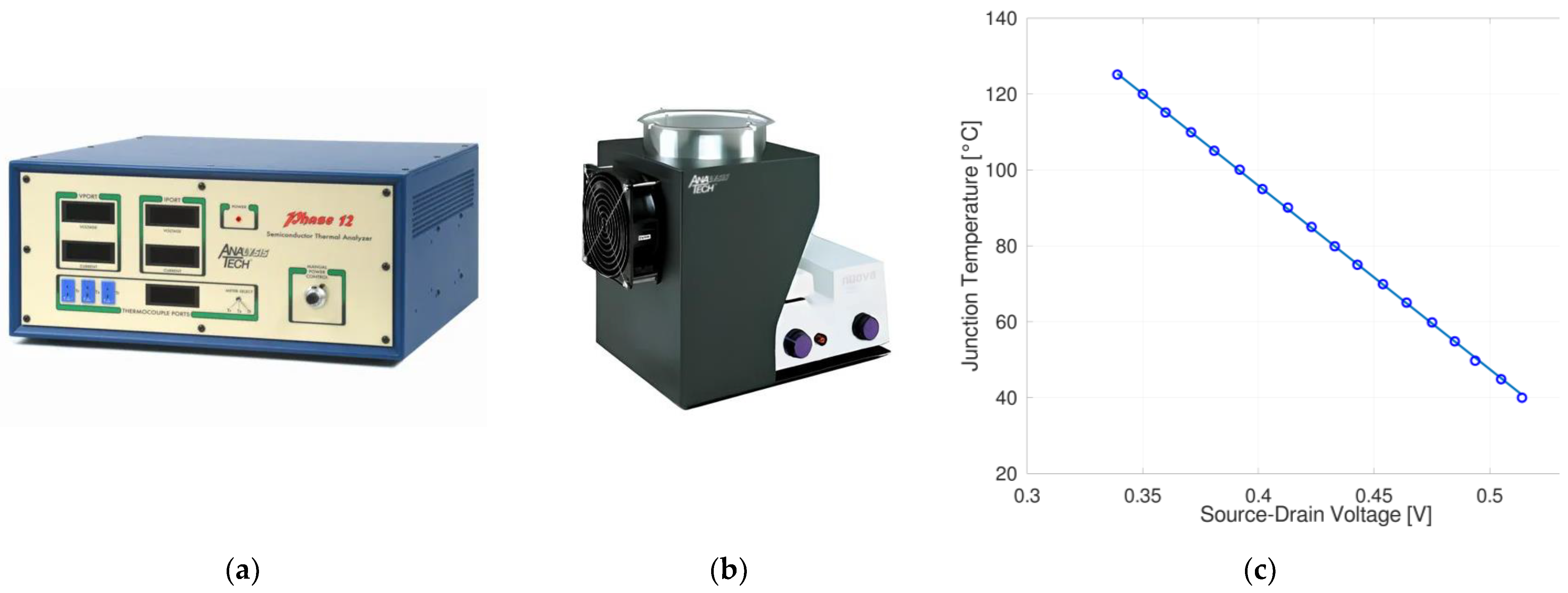
2. MOSFET Junction Temperature Characterization

In this paragraph, the preliminary activities concerning the thermal part and the junction temperature measurement will be covered.
The additional small die MOSFET (MD) was soldered near the device under test (DUT), sharing the same TO247-4 package frame to characterize and then validate the junction temperature estimation. The MOSFET MD was configured as a diode, i.e., a shorting gate and source pads, with the backside (drain) of the die soldered onto the package metal frame. Therefore, in the following, this MOSFET is referred to as an MD diode to easily distinguish it from the main MOSFET.
The 4th lead of the TO247-4 package is wire-bonded to the MD die to externally access its anode (pin A in Figure 1). Generally, commercial products with the TO247-4 package have a different pinout and use the 4th as a Kelvin source to optimize the MOSFET switching. In this case, device assembly is performed only to validate the proposed method.
The characterization phase uses the following four measurement steps:
  • MD diode forward voltage vs. temperature,
  • DUT body diode forward voltage vs. temperature,
  • JEDEC 51-14 transient method on DUT,
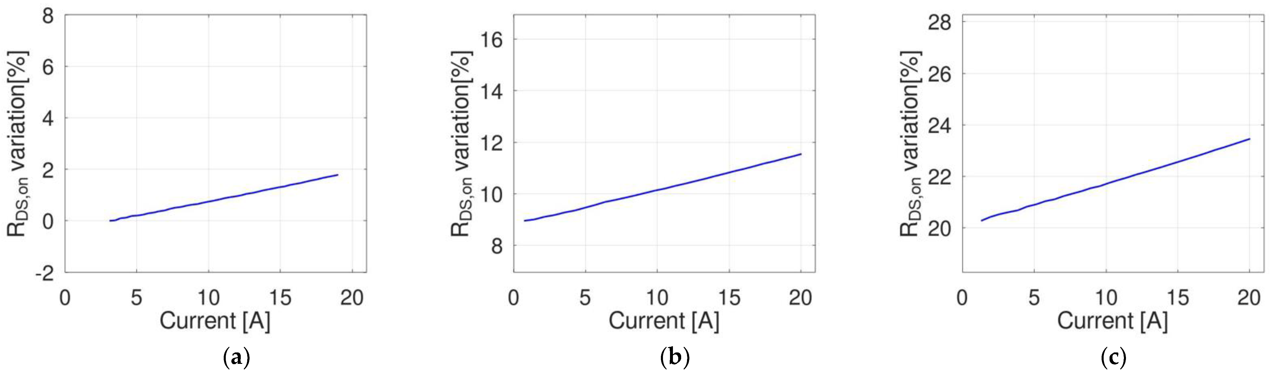
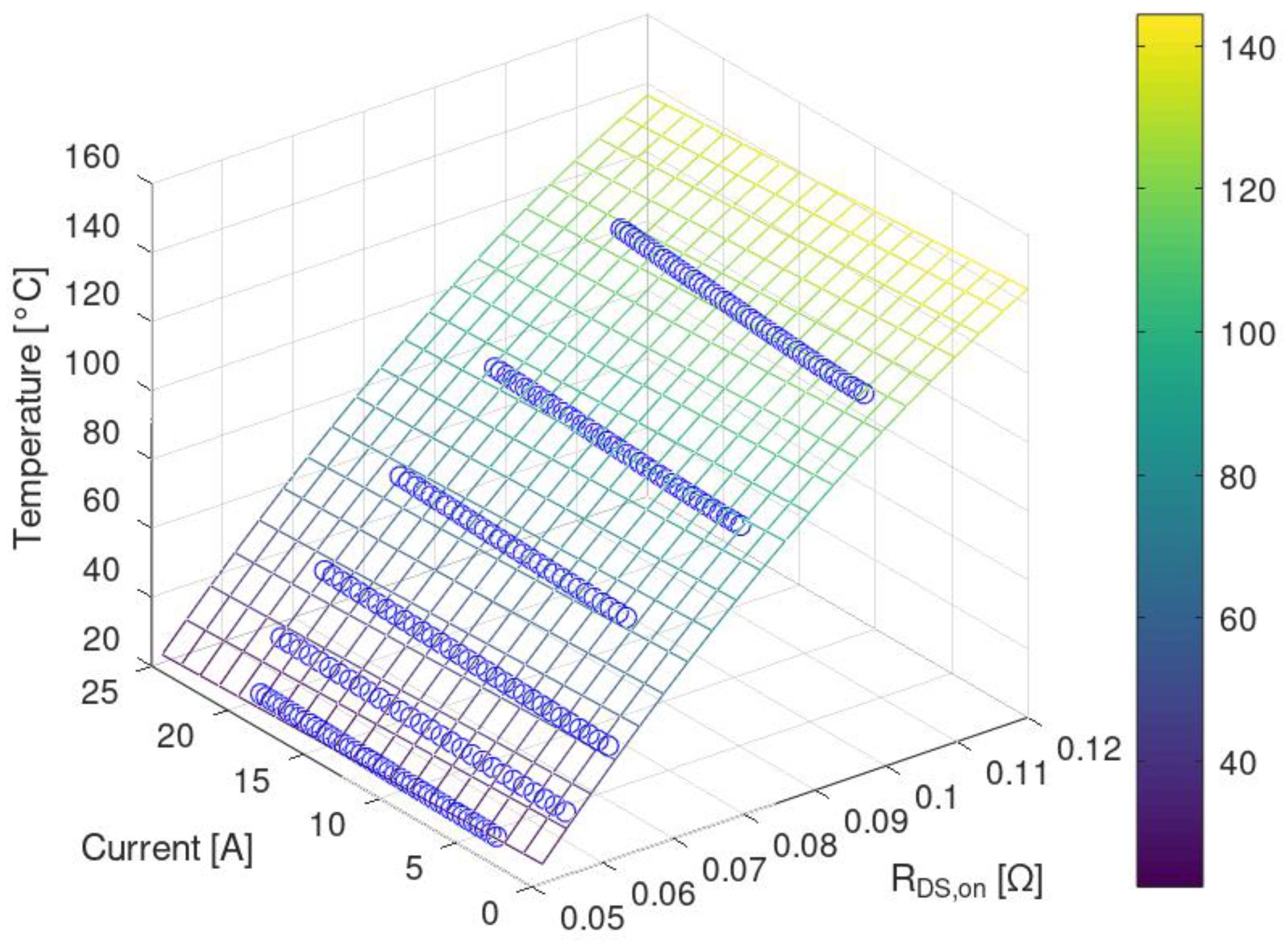
  • DUT RDS,on characterization vs. temperature.

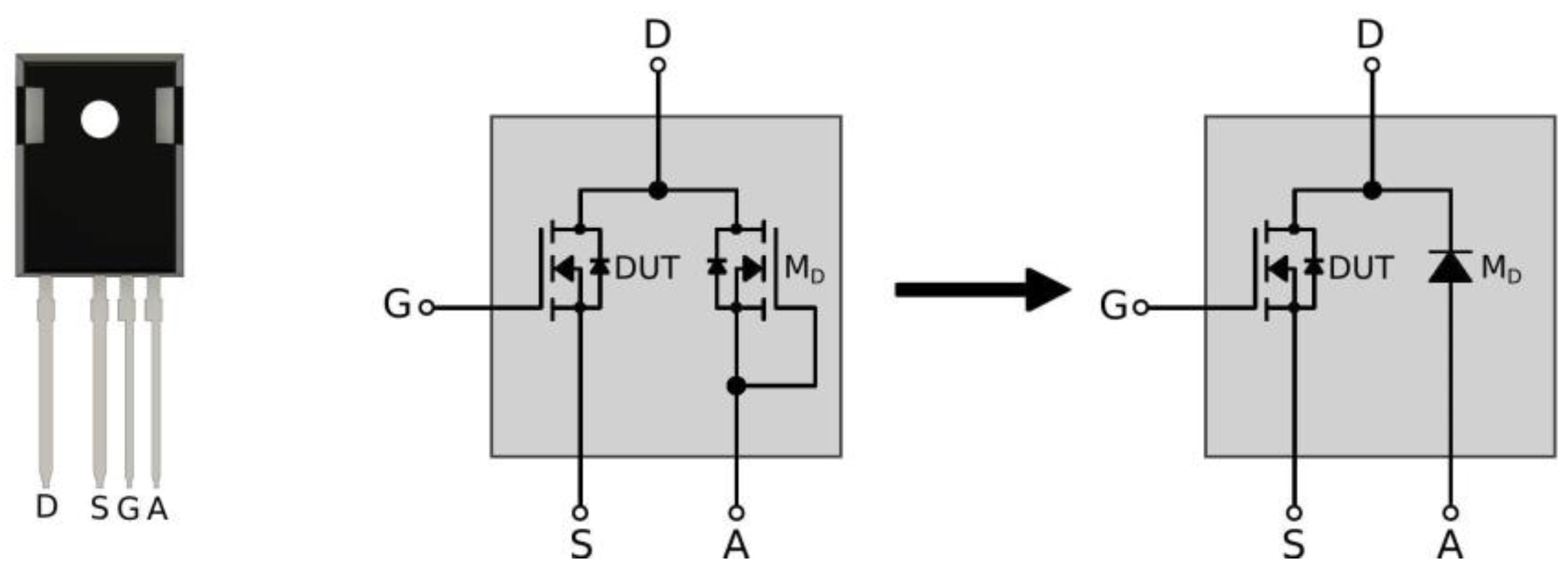
2.1. MD Diode Characterization

First of all, the MD diode forward voltage is characterized as a function of the temperature at a fixed current (5 mA). This measurement is performed using an analysis tech phase 12 thermal analyzer (Figure 2a) with a calibration bath (Figure 2b), in which the device is immersed in a uniform-temperature mineral oil bath to collect data over a range of bath temperatures. This relationship is linear, as shown in Figure 2c, and its linear regression (slope equal to −483.6 °C/V and offset equal to 289.3 °C) is used to exploit the diode as a thermal sensor. The mean and maximum errors due to the linear regression are 0.23 °C and 0.66 °C, respectively.

2.2. DUT Body Diode Characterization and JEDEC 51-1

A thermal analyzer was used to apply the JEDEC 51-1 dynamic mode test to the DUT. In general, this method allows us to evaluate the junction-case or junction-ambient thermal resistance of electronic devices, while in this study, it is used to correlate the junction temperatures between the two dices when the DUT is dissipating some amount of power. This method measures the thermal resistance using the following formula:
R t h = T j T a m b P d i s s
where Tj is the junction temperature, Tamb is the ambient temperature, and Pdiss is the power dissipated by the device. Similar to the MD diode, Tj is calculated using the body diode forward voltage characterization vs. temperature at a fixed current IM.
To measure Tj when the MOSFET is dissipating a certain amount of power through its channel, the body diode should be biased at the current IM when the MOSFET is active; however, this is not feasible. To solve this problem, the JEDEC 51-1 establishes a dynamic mode in which the thermal system must alternately polarize the MOSFET channel and its body diode. The system waveforms are shown in Figure 3. In the interval t 1 , the body diode is polarized at IM to set the initial condition to find the forward voltage VF0 at ambient temperature, which is measured using a thermocouple. During t 2 , VDS is set to VH, and the VGS is adjusted to obtain a constant current IH so as to set the desired dissipated power P d i s s = V H · I H . In the interval t 3 , the body diode is again polarized at IM, obtaining the junction temperature from the difference between VF0 and VFSS and using the slope value of the straight line obtained from the characterization of the body diode. The operations during the intervals t 2 and t 3 are repeated until a thermal steady state is reached. In order to slightly alter the thermal steady state reached during the heating interval t 2 , the interval t 3 has to be much smaller than t 2 . Usually, t 2 is some tens of seconds; instead t 3 is some tens of milliseconds.
This method is normally used to evaluate the thermal resistance while, for this study, it is exploited only for the Tj measurement. The test is set with a DUT dissipating power that gradually increases from 0.5 W to 4 W in order to emulate the power that MOSFETs will dissipate in the converter. During this measurement, the MD diode is also polarized at the same current used during the characterization to measure the forward voltage and, therefore, calculate the temperature. This measurement is compared to the DUT junction temperature, obtaining a small difference (<1 °C). This difference is used as a correction factor that relates the temperature measurement obtained through the MD diode to that of the DUT.

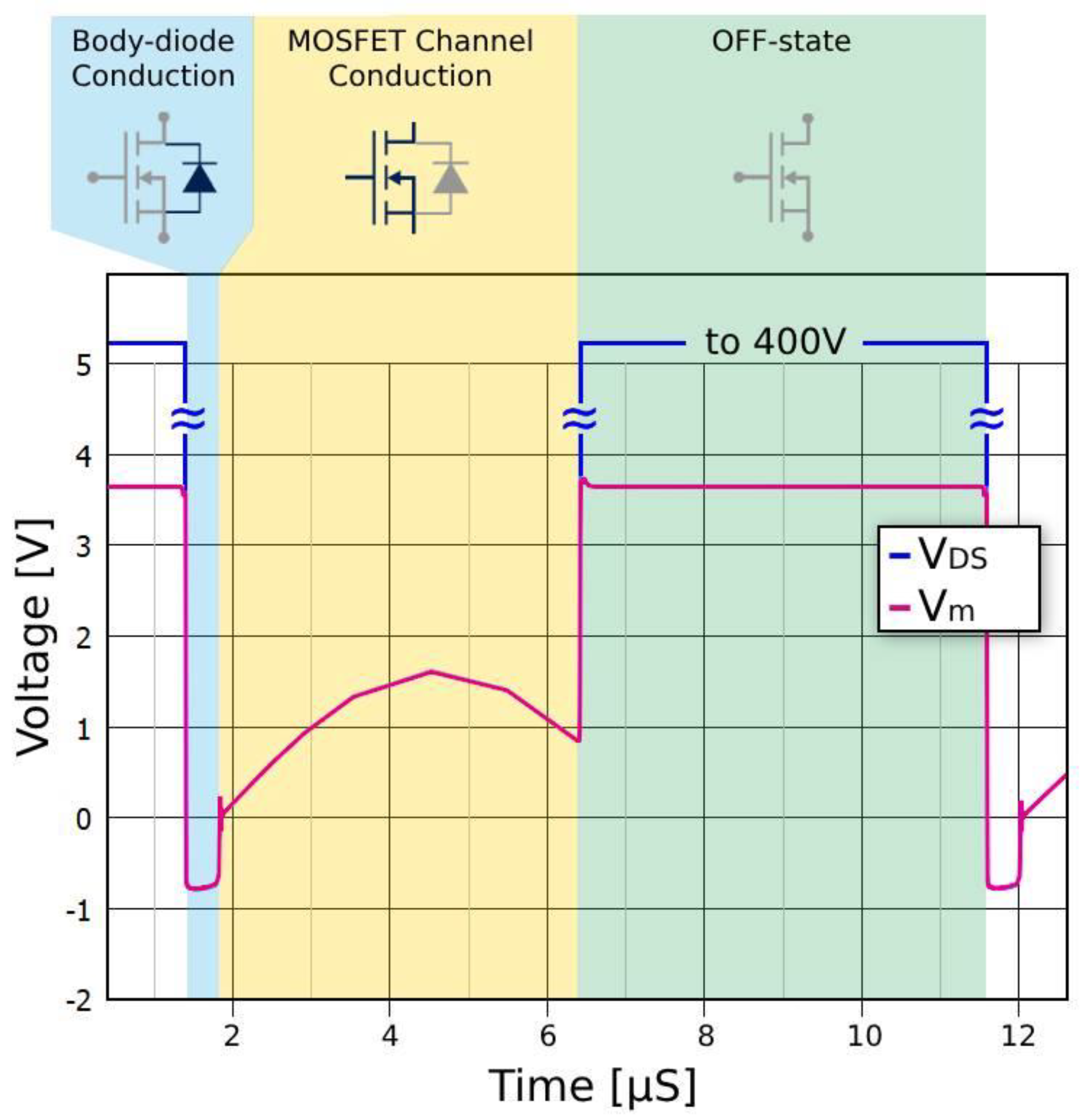
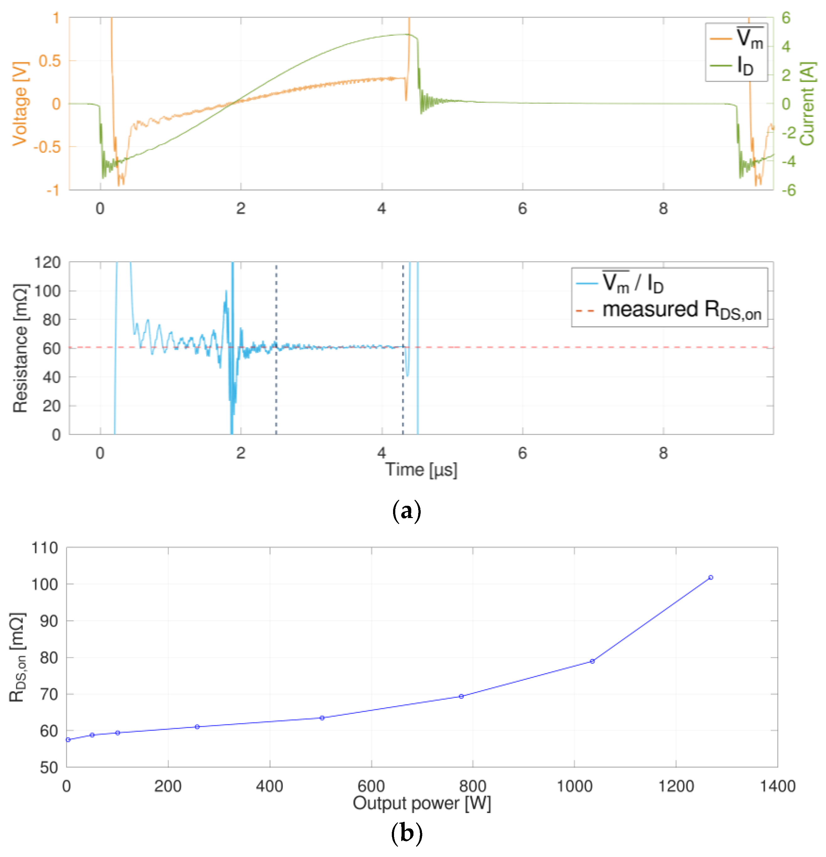
2.3. DUT VDS,on Characterization

The following characterization is used to develop the model for estimating the junction temperature by evaluating the drain-source resistance RDS,on, which is obtained from the measurement of the drain-source voltage and drain current ID. To this aim, the RDS,on of the DUTs was characterized versus drain current ID and junction temperature Tj (Figure 4), as in [23], using the Keysight B1506A curve tracer [24] with an external heater with drain currents up to 20 A.
In this step, the temperature was measured through the MD diode using the previous characterization, without considering the previous correction factor. This factor is not necessary because the temperature is imposed by the heater, and consequently, the MD diode and DUT are in thermal equilibrium. These RDS,on measurements, are used to obtain Tj as a function of RDS,on and ID. The regression used is the following 2nd order polynomial function:
T j R D S , o n , I D = a 1 + a 2 · R D S , o n + a 3 · R D S , o n 2 + a 4 · I D + a 5 · R D S , o n · I D
with a 1   , , a 5   are the polynomial coefficients of the function, equal to, respectively, −117.4573, 3229.3406, −8725.5927, 0.0043993, −2.6674.
The resulting function is illustrated in Figure 5. This function was mathematically validated using the results shown in Figure 4. Figure 6 shows the temperature estimated (blue circle) for different junction temperatures (green line). Table 1 reports, for each temperature, the maximum error together with the current at which the maximum error occurs.

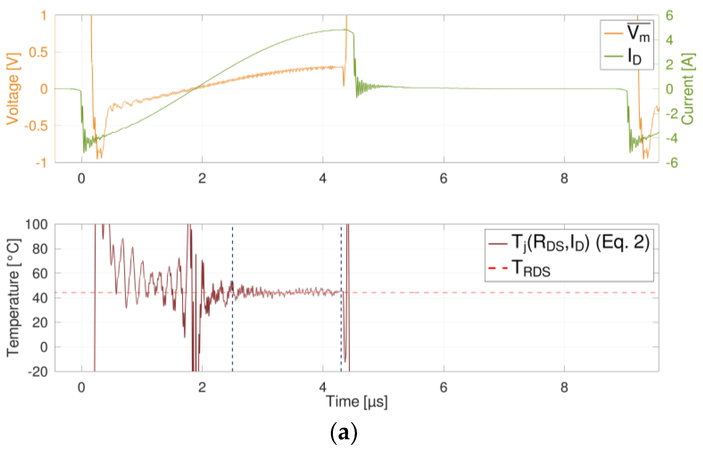
3. Evaluation of the On-State Resistance Used for Junction Temperature Estimation

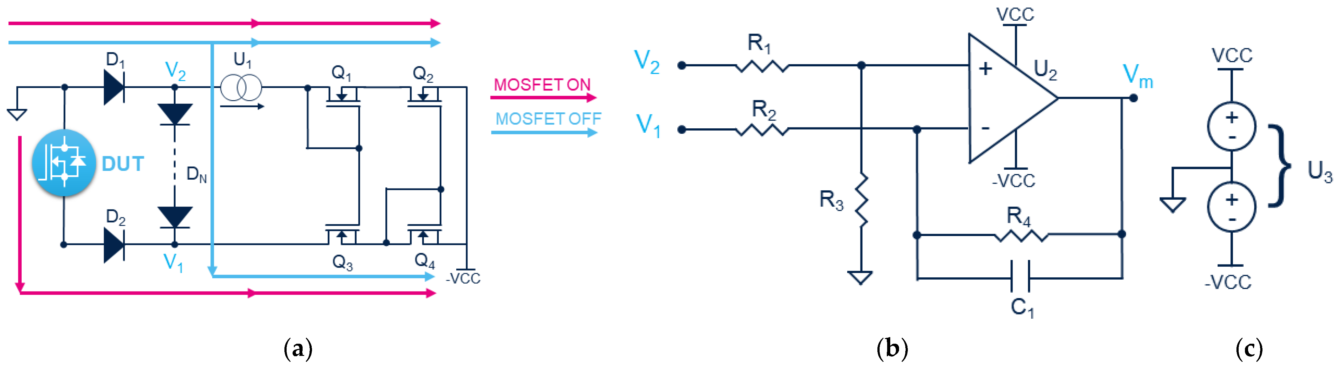
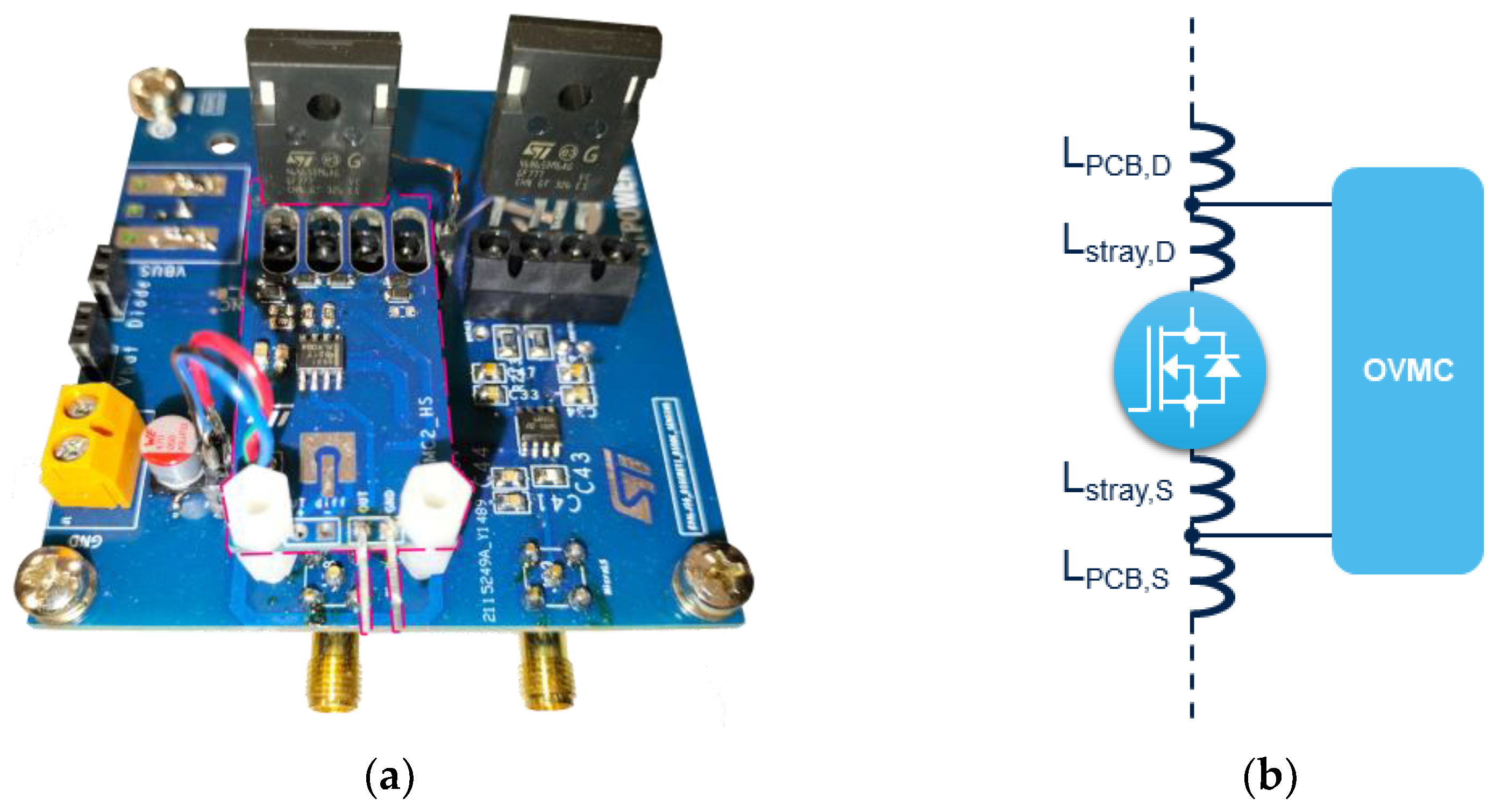
3.1. On-Voltage Measurement Circuit

The value of RDS,on can be estimated from the relationship between on-state voltage and current measurements. A Tektronix TCP0030A current probe has been used for the current measurement. The use of an oscilloscope and high-voltage probe to measure the on-state voltage in a high-voltage circuit leads to inaccurate values. Therefore, an on-state voltage measurement circuit (OVMC) is required [14]. The output of the OVMC (Vm) limits the VDS voltage variation (Figure 7) to improve the accuracy of the voltage measurement by setting a smaller vertical scale.
The measurement of the on-state voltage presents several challenges in terms of accuracy and high blocking voltage capability. Moreover, the high switching frequencies of modern power devices require an extremely fast dynamic response.
In the half-bridge (HB) LLC, the MD diode was not used as the thermal sensor of the low-side (LS) MOSFET because of the drain voltage; consequently, the MD cathode potential swings from 0 V to the BUS voltage (400 V). The voltage transient at the middle point, associated with the stray elements, is considered a potential source of noise. For this reason, the measurement of the voltage with MD was performed only for the high-side (HS) MOSFET where the MD cathode voltage is fixed at VBUS. Therefore, the OVMC circuit has been designed for the HS MOSFET. The OVMC final circuit is shown in Figure 8.
Table 2 reports the characteristics and values of the devices used. The OVMC with these devices presents a 600 V maximum drain voltage. To increase this voltage is sufficient to choose D1 and D2 diodes with a higher voltage or insert more diodes in series or, in other types of circuits, increase the number of clamping stages [25].
The basic circuit is proposed in [26,27] but, in this study, several changes have been made. The schematic has been mirrored to have a reference point on the drain rather than on the source [12,13,18]. Moreover, transistors Q1, Q2, Q3, and Q4 are MOSFET instead of BJTs and form a Wilson current mirror instead of a cascode mirror. Finally, the biasing resistor has been replaced with a constant current driver.
The diode D1 is always polarized by U1 at about 10 mA. When the DUT is ON, D2 is polarized with the same current as D1 owing to the current mirror (purple line in Figure 8a), and when the DUT is OFF, the series of diodes DN is polarized with the same current as U1 (light blue line in Figure 8a). The number of diodes, DN, changes based on the application and MOSFET RDS,on and define the clamp voltage of the OVMC. In this work, there are six diodes.
The op-amp circuit (Figure 8b) is a differential stage that provides the difference between V2 and V1; therefore, during the on-state, the output Vm is:
V m = V 2 V 1 = V D 1 ( V D S , o n V D 2 )
Considering that D1 and D2 are polarized in the same way, i.e., V D 1 V D 2 , then:
V m = V D S , o n
Therefore, the OVMC output is V D S , o n plus an offset due to op-amp and a slight difference between the diodes’ forward voltage VD.
An isolated dual-output 12V DC-DC converter (Figure 8c) is used to supply the OVMC board. An isolated converter permits to follow the VDS signal better, avoiding a voltage drop on the drain line. Unlike in [28], where there is an active circuit to subtract this voltage.
An important challenge when reading the OVMC output Vm is that this signal refers to the drain voltage of HS MOSFET, which is usually connected to the input voltage. To read this voltage, a low-voltage differential probe with a high common mode voltage must be used. Usually, low-voltage differential probes have low common mode voltages unless an opto-isolated probe is used [27]. To avoid this problem, the oscilloscope ground is connected to the drain reference in order to cancel the common mode voltage of the low-voltage differential probe, as shown in Figure 9.
Moreover, the OVMC allows for accurately measuring the power dissipated on the body diode (in ZVS converter) and the conduction losses of the MOSFET; therefore, a further characteristic of OVMC is that of being able to read both positive and negative voltage, unlike the circuit proposed in [25].

3.2. LLC Converter

In this work, condition monitoring is applied to a resonant converter in the telecom market. Therefore, the OVMC was adopted in a 1500 W LLC converter. This type of converter has been chosen as the current changes its polarity; the zero-crossing point is fundamental for the calibration, as will be explained later.
A typical LLC converter for the telecom market with the following characteristics has been realized:
  • Input voltage: 400 V ± 1%
  • Maximum output power: 1500 W
  • Output voltage: 48 V ± 1%
  • Maximum output current: 31.25 A
  • Efficiency (at maximum load): ≥95%
  • Resonant frequency: 102.73 kHz
LLC converter is a high-power buck converter. In this case, a half-bridge converter is used, and its schematic is shown in Figure 10a. The two MOSFETs Q1 (high-side HS) and Q2 (low-side LS) commutate at a high frequency with the same on-time TON. The operation exploits the resonance of LLC circuits, which are composed of LR, LM, and CR.
The output voltage is determined by the following formula:
V o u t = M g · 1 n · V i n 2
where Mg is the gain of the LLC tank, which depends on the switching frequency, and n is the transformer turns ratio. The switching frequency changes to the right of the gain curve peak, as shown in Figure 10b, and as it approaches the curve peak, the output power increases. Working on the right side of the curve allows us to achieve zero voltage switching (ZVS) conditions during turn-on.
Figure 11 shows a typical LLC converter switching period with VDS, OVMC output Vm, and the three MOSFET operating areas. During dead time, the body diode conducts, which permits it to reach ZVS (blue area). After that, the MOSFET turn-on occurs, and the current passes through its channel with a drain voltage that follows the current shape (yellow area). Finally, the MOSFET is turned off (green area), and the complementary MOSFET follows the behavior related to the blue area. At low power, the current shape is triangular, and once the frequency approaches the peak of the gain curve, the current becomes sinusoidal.

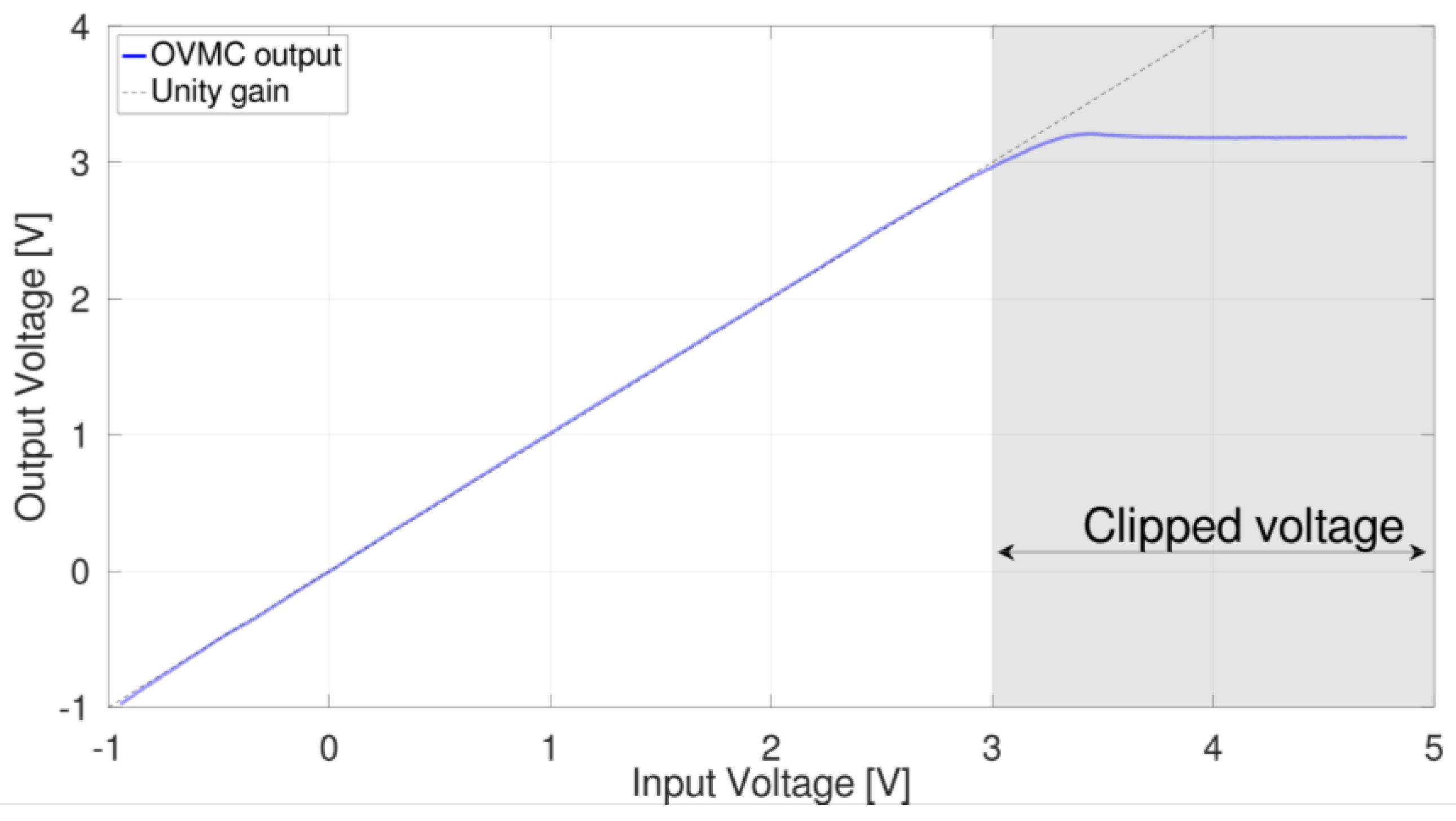
3.3. OVMC Compensation in LLC Converter

Due to the non-idealities of the operational amplifier and resistors, the gain is not unitary. To evaluate the actual value, the VDS input of the OVMC is connected to a waveform generator that generates a triangular waveform. By comparing this input signal with the Vm output signal from the clipped zone, the real gain can be calculated, from which a corrective factor to account for the oscilloscope measurements is obtained.
The OVMC measures the on-state voltage across the DUT leads. Therefore, the Vm voltage is equal to VDS,on plus the voltage across the parasitic inductance of the DUT wire bonding and leads [29]. For this reason, the OVMC must be soldered close to the package, as shown in Figure 12a. The different contributions are shown in Figure 12b, where LPCB,D and LPCB,S incorporate the drain and source stray inductance of the PCB trace, connectors, and DUT leads, while Lstray,D and Lstray,S represent the drain and source stray inductances. The latter contributions are indistinguishable, and consequently, they are considered as a whole parasitic inductance Lstray:
L s t r a y = L s t r a y , D + L s t r a y , S
Moreover, Vm also includes a small offset due to either the operational amplifier stage or the differential probe Tektronix TDP1500 used. To compensate for the extra voltage caused by Lstray, it is subtracted mathematically using an oscilloscope.
V D S , o n = V m V o f f s e t L s t r a y d I D d t
The quantity L s t r a y can be obtained by physical simulations or experimental waveforms. In order to obtain a resistive load, I D and V D S , o n must be in phase, and therefore, the zero-crossing of the current and voltage must coincide. As shown in Figure 13a, the zero-crossing of ID does not coincide with that of Vm. Therefore, L s t r a y and V o f f s e t can be extracted from waveforms at two different converter power levels P 1 and P 2 . Changing the output power level, the d I D / d t also changes, and therefore, it is possible to distinguish V o f f s e t from L s t r a y d I D d t as follows.
For the first output level P o u t = P 1 , the V m signal at I D = 0 is
V m ( 1 ) | I D = 0 = V o f f s e t + L s t r a y d I D ( 1 ) d t
where V m | I D = 0 and d I D / d t can be measured with an oscilloscope, and thus, they will be the known terms.
For the second output level P o u t = P 2 , in the same way, it can be written as
V m ( 2 ) | I D = 0 = V o f f s e t + L s t r a y d I D ( 2 ) d t
In this way a system with two equations and two unknowns can be obtained as
V m ( 1 ) | I D = 0 = V o f f s e t + L s t r a y d I D ( 1 ) d t , P o u t = P 1 V m ( 2 ) | I D = 0 = V o f f s e t + L s t r a y d I D ( 2 ) d t , P o u t = P 2
Solving the system provides the value of V o f f s e t and L s t r a y . The compensated V m ¯ voltage is
V m ¯ = V m V o f f s e t L s t r a y d I D d t
In this way, V o f f s e t accounts for the OVMC, the differential voltage probe, and the current probe offset voltages. In the prototype, L s t r a y 9 n H .
The waveform with this correction is shown in Figure 13a, highlighting the in-phase current and voltage. Figure 14a,b show the waveforms at full load without and with this correction. Under this condition, the converter operates in a quasi-sinusoidal steady state, and consequently, the lack of correction also leads to a shift in the voltage peak relative to the current peak.

4. Condition Monitoring of the Resonant Converter by Combining the MOSFET Junction Temperature Characterization and OVMC

The MOSFETs used in this LLC converter are two STWA46N65DM6, 650 V devices with RDS,on(typ) = 55 mΩ. The compensation techniques described previously are extremely important in this case because the low RDS,on could lead to inaccurate on-state voltage measurement since it is small. The MOSFET RDS,on is directly evaluated using the oscilloscope Tektronix MSO66B that measures V m ¯ and ID (Figure 15a). The light blue waveform in Figure 15 represents the RDS,on and it diverges when ID approaches zero, as division by zero is carried out. This divergence causes an oscillation, and therefore, the RDS,on value is calculated after damping by the mean value between the two dashed lines. The measured RDS,on vs. POUT is shown in Figure 15b. From the inspection of Figure 15a, it is apparent that possible Vm spikes and oscillations during the switching transient do not affect the estimation because they are executed inside the MOSFET conduction interval (inside the dashed lines). Moreover, these spikes and oscillations do not affect circuit operation because they do not exceed the components’ safe-operating-area.
As previously mentioned, to validate the temperature estimation through resistance measurement, a diode was inserted inside the package. As the MD cathode is connected to the DUT drain, Vf cannot be measured at the drain lead because it also includes the voltage drop at the drain lead caused by the current flowing on the DUT MOSFET. To avoid this problem, an additional wire is soldered onto the frame behind the MD die.
The MD diode is polarized at a 5 mA current with an LD1117STR based circuit with a constant current configuration. The MD Vf was monitored with a Keithley DMM6500 6.5-digit multimeter running a dedicated script that instantly converted the measured voltage into temperature (Figure 16).
In the beginning, Vf is associated with ambient temperature measured through a thermocouple. Then, the correction factor described in Section 2.1 is used to relate the diode temperature with the DUT junction temperature. Finally, the temperature has been calculated using the previous characterization of the MD diode forward voltage vs. temperature reported in Figure 2c.
Equation (2) is used to estimate Tj from the RDS,on measurement, as shown in Figure 17, considering two different output power levels. In detail, Equation (2) is calculated using the oscilloscope (brown waveform), and the mean of the values between the two vertical dashed lines is the estimated Tj, called TRDS, and is indicated by the red dashed lines. In Figure 17, the temperature calculated between the cursors is almost constant, thus confirming the goodness of the regression function for all current shapes and at different LLC converter output powers.
During the LLC converter operation, Pout gradually increased, and the measurements were acquired at a thermal steady state. The measurements were halted when the MOSFETs were overheated at 120 °C. The TRDS results compared to the temperature measured by the MD diode are shown in Figure 18. The figure shows a ΔT of 0.35 °C as the maximum error between the two measures.

5. Conclusions

In the semiconductor industry, the junction temperature in a MOSFET is directly obtained through the thermal characterization of its body diode, as established by JEDEC 51–14. This measurement is not practical when the MOSFET operates in a resonant converter. In this work, the MOSFET junction temperature was measured using two approaches. One is based on the variation in the forward voltage of a diode (direct method), and the other exploits the electrical measurements obtained through an OVMC (indirect method). Starting from electrical measurements, the proposed method based on the OVMC allows us to track the HS MOSFET junction temperature while an LLC power converter is running. The junction temperature derived using this indirect method was compared with that derived using the direct method and considered as a reference because it exploits a simultaneous thermal value retrieved from an additional MOSFET housed inside the same package used as a thermal sensor.
The junction temperature estimation of OVMC was compared with that of the direct method for accuracy verification. The results confirm the effectiveness of the proposed approach (maximum error of less than 1%).
The proposed approach is simpler because it can be applied to any MOSFET without the need for specific assemblies. Furthermore, the OVMC refers exactly to the junction temperature of the die under test, while the diode method measures the temperature of a die near the DUT.
Furthermore, the use of the OVMC allows monitoring of the junction temperature during any operating condition of the resonant converter. Hence, condition monitoring anticipates the potential risks of MOSFET failure. An additional advantage is the on-line monitoring of the RDS, which enables the identification of potential degradation and aging of the MOSFET, and then performs predictive maintenance. Another advantage is the potential use of OVMC to measure conduction losses and body diode losses. Therefore, this technique can also be used for characterization and modeling of MOSFETs operating in resonant converters.

Author Contributions

Conceptualization, M.V. and A.S.; Data curation, M.V. and G.S.; Formal analysis, A.S.; Investigation, G.B.; Methodology, M.V., A.S. and F.I.; Supervision, A.S. and S.A.R.; Validation, G.S.; Visualization, M.V.; Writing—original draft, M.V. and A.S.; Writing—review & editing, M.V., F.I. and S.A.R. All authors have read and agreed to the published version of the manuscript.

Funding

This research received no external funding.

Data Availability Statement

Data are contained within the article.

Conflicts of Interest

Marco Ventimiglia, Alfio Scuto, Giuseppe Sorrentino, and Gaetano Belverde were employed by the company ST Microelectronics Co., Ltd. Francesco Iannuzzo and Santi Agatino Rizzo declare that the research was conducted in the absence of any commercial or financial relationships that could be construed as potential conflicts of interest.

References

  1. Kumar, A.; Moradpour, M.; Losito, M.; Franke, W.-T.; Ramasamy, S.; Baccoli, R.; Gatto, G. Wide Band Gap Devices and Their Application in Power Electronics. Energies 2022, 15, 9172. [Google Scholar] [CrossRef]
  2. Rizzo, S.A.; Salerno, N. Actual reasons involving turn-off losses improvement with increasing load and gate resistance in MOSFETs enhanced with Kelvin source. IEEE Trans. Ind. Electron. 2024, 71, 369–379. [Google Scholar] [CrossRef]
  3. Roccaforte, F.; Fiorenza, P.; Greco, G.; Nigro, R.L.; Giannazzo, F.; Iucolano, F.; Saggio, M. Emerging trends in wide band gap semiconductors (SiC and GaN) technology for power devices. Microelectron. Eng. 2018, 187–188, 66–77. [Google Scholar] [CrossRef]
  4. Adragna, C. LLC Resonant Converters: An Overview of Modeling, Control and Design Methods and Challenges. Found. Trends® Electr. Energy Syst. 2022, 5, 75–491. [Google Scholar] [CrossRef]
  5. Nguyen, M.H.; Kwak, S. Enhance Reliability of Semiconductor Devices in Power Converters. Electronics 2020, 9, 2068. [Google Scholar] [CrossRef]
  6. Martínez, J.; Riba, J.-R.; Moreno-Eguilaz, M. State of Health Prediction of Power Connectors by Analyzing the Degradation Trajectory of the Electrical Resistance. Electronics 2021, 10, 1409. [Google Scholar] [CrossRef]
  7. Rizzo, S.A.; Susinni, G.; Iannuzzo, F. Intrusiveness of Power Device Condition Monitoring Methods: Introducing Figures of Merit for Condition Monitoring. IEEE Ind. Electron. Mag. 2022, 16, 60–69. [Google Scholar] [CrossRef]
  8. Bayerer, R.; Herrmann, T.; Licht, T.; Lutz, J.; Feller, M. Model for Power Cycling lifetime of IGBT Modules—Various factors influencing lifetime. In Proceedings of the 5th International Conference on Integrated Power Electronics Systems, Nuremberg, Germany, 11–13 March 2008; pp. 1–6. [Google Scholar]
  9. Junghaenel, M.; Schmidt, R.; Strobel, J.; Scheuermann, U. Investigation on Isolated Failure Mechanisms in Active Power Cycle Testing. In Proceedings of the PCIM Europe 2015; International Exhibition and Conference for Power Electronics, Intelligent Motion, Renewable Energy and Energy Management, Nuremberg, Germany, 19–20 May 2015; pp. 1–8. [Google Scholar]
  10. Duan, Y.; Kang, J.; Shi, Y.; Xin, Z. An Online On-State Voltage Measurement Circuit With Series Diode Clamp for SiC MOSFETs. CPSS Trans. Power Electron. Appl. 2023, 8, 23–32. [Google Scholar] [CrossRef]
  11. Baker, N.; Luo, H.; Iannuzzo, F. Simultaneous On-State Voltage and Bond-Wire Resistance Monitoring of Silicon Carbide MOSFETs. Energies 2017, 10, 384. [Google Scholar] [CrossRef]
  12. Hosseinabadi, F.; Jaman, S.; Bhoi, S.K.; Hasan, M.M.; Chakraborty, S.; El Baghdadi, M.; Hegazy, O. Implementation of onsite Junction Temperature Estimation for a SiC MOSFET Module for Condition Monitoring. In Proceedings of the 2022 24th European Conference on Power Electronics and Applications (EPE’22 ECCE Europe), Hanover, Germany, 5–9 September 2022; pp. P.1–P.6. [Google Scholar]
  13. Hong, K.; Chen, X.Y.; Chen, Y.; Zhang, M.S.; Wang, J.L.; Jiang, S.; Pang, Z.; Yang, H.M.; Xue, N.; Gou, H.Y.; et al. Experimental Investigations Into Temperature and Current Dependent On-State Resistance Behaviors of 1.2 kV SiC MOSFETs. IEEE J. Electron Devices Soc. 2019, 7, 925–930. [Google Scholar] [CrossRef]
  14. Zhang, Q.; Zhang, P. A Novel Model of the Aging Effect on the ON-State Resistance of SiC Power MOSFETs for High-Accuracy Package-Related Aging Evaluation. IEEE Trans. Ind. Electron. 2023, 70, 9495–9504. [Google Scholar] [CrossRef]
  15. Zhang, Q.; Yang, Y.; Zhang, P. A Novel Method for Monitoring the Junction Temperature of SiC MOSFET On-line Based on On-state Resistance. In Proceedings of the 2019 22nd International Conference on Electrical Machines and Systems (ICEMS), Harbin, China, 11–14 August 2019; pp. 1–5. [Google Scholar]
  16. Ye, Z.; Zheng, Z.; Li, C. A New Measurement of Online Junction Temperature Based on On-state Resistance. In Proceedings of the 2023 IEEE 6th International Electrical and Energy Conference (CIEEC), Hefei, China, 12–14 May 2023; pp. 3367–3370. [Google Scholar]
  17. Stella, F.; Pellegrino, G.; Armando, E.; Daprà, D. Online Junction Temperature Estimation of SiC Power MOSFETS through On-State Voltage Mapping. IEEE Trans. Ind. Appl. 2018, 54, 3453–3462. [Google Scholar] [CrossRef]
  18. Magnone, P.; Petucco, A.; Thevenet, N.; Abedini, H. Simplified on-line monitoring system of MOSFET on-resistance based on a semi-empirical model. In Proceedings of the 2019 IEEE Applied Power Electronics Conference and Exposition (APEC), Anaheim, CA, USA, 17–21 March 2019; pp. 2746–2750. [Google Scholar]
  19. Sirat, A.P.; Roy, C.; Evans, D.; Gafford, J.; Parkhideh, B. In-Situ Ultrafast Sensing Techniques for Prognostics and Protection of SiC Devices. In Proceedings of the 2022 IEEE 9th Workshop on Wide Bandgap Power Devices & Applications (WiPDA), Redondo Beach, CA, USA, 7–9 November 2022; pp. 142–147. [Google Scholar]
  20. Roy, C.; Kim, N.; Evans, D.; Sirat, A.P.; Gafford, J.; Parkhideh, B. A Half-Bridge On-State Voltage Sensor for In-Situ Measurements. In Proceedings of the 2022 IEEE Energy Conversion Congress and Exposition (ECCE), Detroit, MI, USA, 9–13 October 2022; pp. 1–7. [Google Scholar]
  21. Roy, C.; Kim, N.; Gafford, J.; Parkhideh, B. On-State Voltage Measurement of High-Side Power Transistors in Three-Phase Four-Leg Inverter for In-Situ Prognostics. In Proceedings of the 2021 IEEE Energy Conversion Congress and Exposition (ECCE), Vancouver, BC, Canada, 10–14 October 2021; pp. 2770–2776. [Google Scholar]
  22. Scuto, A.; Sorrentino, G.; Ventimiglia, M.; Belverde, G.; Nardo, D.; Vitale, G.; Lullo, G. Assessment of MOSFET switching losses in an LLC converter by a calorimetric method. In Proceedings of the 2023 IEEE Applied Power Electronics Conference and Exposition (APEC), Orlando, FL, USA, 19–23 March 2023; pp. 2456–2462. [Google Scholar]
  23. Zhang, Q.; Lu, G.; Yang, Y.; Zhang, P. A High-Frequency Online Junction Temperature Monitoring Method for SiC mosfets Based on on-State Resistance With Aging Compensation. IEEE Trans. Ind. Electron. 2023, 70, 7393–7405. [Google Scholar] [CrossRef]
  24. B1506A Power Device Analyzer/Curve Tracer for Circuit Design. Available online: https://www.keysight.com/dk/en/product/B1506A/power-device-analyzer-curve-tracer-circuit-design.html (accessed on 17 September 2024).
  25. Barón, K.M.; Weiser, M.C.J.; Sharma, K.; Kallfass, I. Analysis of a Transistor-Based On-State Voltage Measurement Circuit for Condition Monitoring of Power Transistors. In Proceedings of the 2023 IEEE Applied Power Electronics Conference and Exposition (APEC), Orlando, FL, USA, 19–23 March 2023; pp. 2556–2562. [Google Scholar]
  26. Gelagaev, R.; Jacqmaer, P.; Driesen, J. A Fast Voltage Clamp Circuit for the Accurate Measurement of the Dynamic ON-Resistance of Power Transistors. IEEE Trans. Ind. Electron. 2015, 62, 1241–1250. [Google Scholar] [CrossRef]
  27. Weiser, M.C.J.; Barón, K.M.; Fink, T.; Kallfass, I. A Fast ON-State Drain-to-Source Voltage Amplifier for the Dynamic Characterization of GaN Power Transistors. In Proceedings of the 2023 IEEE Applied Power Electronics Conference and Exposition (APEC), Orlando, FL, USA, 19–23 March 2023; pp. 637–644. [Google Scholar]
  28. Rossetto, L.; Spiazzi, G. A Fast ON-State Voltage Measurement Circuit for Power Devices Characterization. IEEE Trans. Power Electron. 2022, 37, 4926–4930. [Google Scholar] [CrossRef]
  29. Guacci, M.; Bortis, D.; Kolar, J.W. On-state voltage measurement of fast switching power semiconductors. CPSS Trans. Power Electron. Appl. 2018, 3, 163–176. [Google Scholar] [CrossRef]
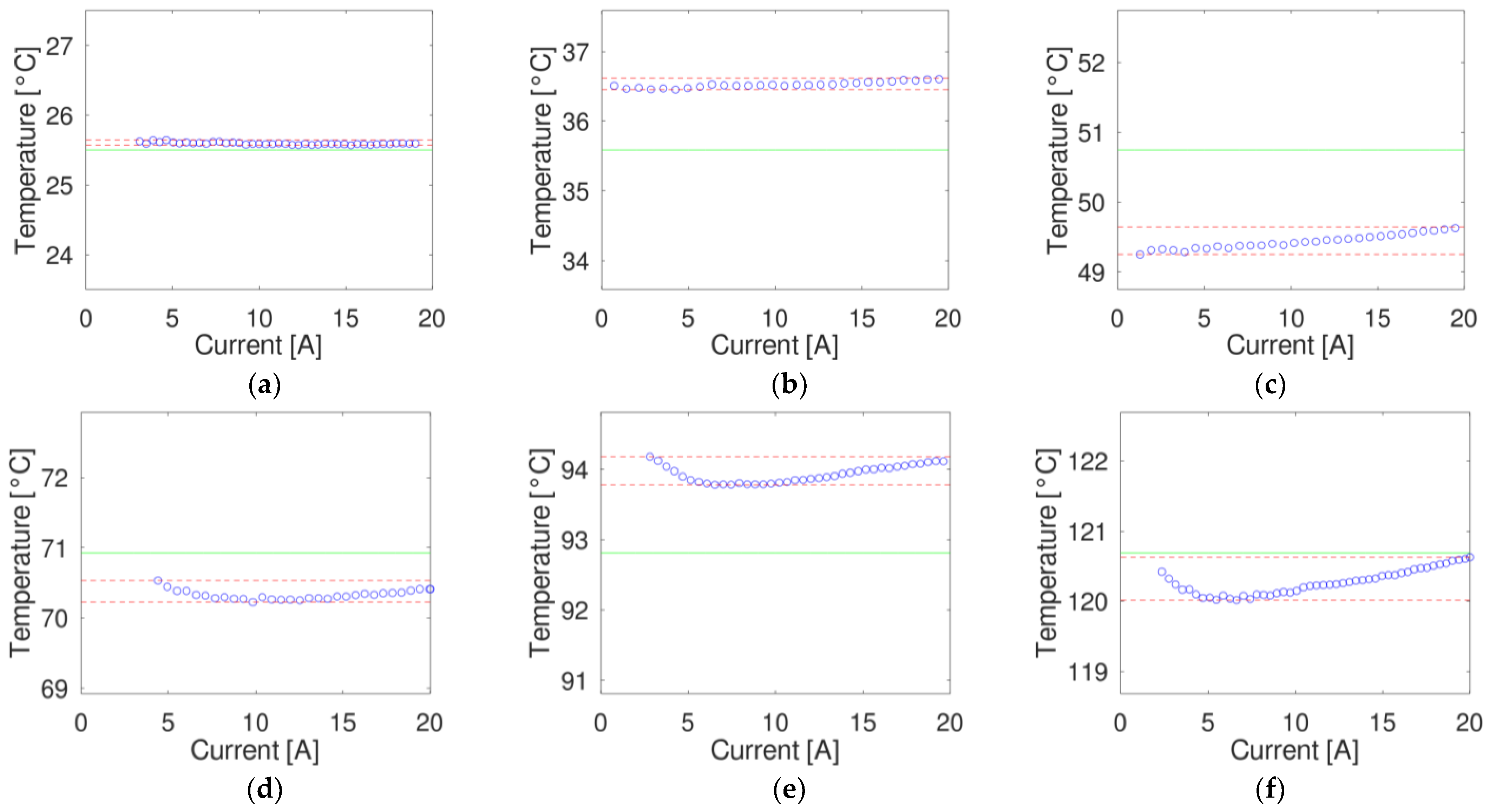
Figure 1. Assembled device with its pinout and internal configuration.
Electronics 13 03902 g001
Figure 2. Analysis tech phase 12 thermal analyzer with results: (a) thermal analyzer main unit, (b) calibration bath, and (c) MD diode forward voltage vs. temperature.
Electronics 13 03902 g002
Figure 3. JEDEC 51-1 dynamic mode waveforms with MOSFETs.
Electronics 13 03902 g003
Figure 4. RDS,on characterization with drain current variation at different temperatures: (a) 25.5 °C, (b) 35.6 °C, (c) 50.7 °C, (d) 70.9 °C, (e) 92.8 °C, (f) 120.7 °C.
Electronics 13 03902 g004aElectronics 13 03902 g004b
Figure 5. Temperature regression as a function of RDS,on, and ID. The blue circles represent the measured values.
Electronics 13 03902 g005
Figure 6. Temperature estimated using Equation (2), the values of RDS,on, and ID reported in Figure 4 (blue circles) vs. the actual temperature (green). The red dotted lines indicate the minimum and maximum errors. (a) 25.5 °C, (b) 35.6 °C, (c) 50.7 °C, (d) 70.9 °C, (e) 92.8 °C, (f) 120.7 °C.
Electronics 13 03902 g006
Figure 7. OVMC output vs. input voltage.
Electronics 13 03902 g007
Figure 8. Proposed OVMC: (a) main circuit and stages of operation, (b) operational amplifier circuit, and (c) power circuit.
Electronics 13 03902 g008
Figure 9. Ground connection between the half-bridge board and oscilloscope. NOTE: VBUS power supply is isolated from the ground.
Electronics 13 03902 g009
Figure 10. Half-Bridge LLC converter: (a) schematic and (b) gain curve.
Electronics 13 03902 g010
Figure 11. Typical LLC converter switching period VDS with OVMC output Vm and highlighted MOSFET operating area.
Electronics 13 03902 g011
Figure 12. HB board prototype. (a) OVMC board on prototype (b) representation of DUT and board parasitic inductances with OVMC connection.
Electronics 13 03902 g012
Figure 13. LLC waveforms. Drain current in green, Vm output in yellow. (a) without OVMC compensation and (b) with OVMC compensation.
Electronics 13 03902 g013
Figure 14. LLC waveforms at full load. Drain current in green, Vm output in yellow. (a) without OVMC compensation and (b) with OVMC compensation.
Electronics 13 03902 g014
Figure 15. RDS,on evaluation (a) LLC waveforms at 250 W: Drain current in green, V m ¯ output in yellow, V m ¯ / I D in light blue, measured RDS,on in red dashed line. (b) RDS,on variation as a function of the LLC output power.
Electronics 13 03902 g015
Figure 16. Keithley DMM6500 multimeter running the custom script.
Electronics 13 03902 g016
Figure 17. LLC waveforms at two power levels: (a) 250 W and (b) 1280 W. Drain current in green, V m ¯ output in yellow, Tj estimated using Equation (2) in brown, and calculated TRDS in a red dashed line.
Electronics 13 03902 g017aElectronics 13 03902 g017b
Figure 18. Comparison between the value of Tj estimated using the proposed approach based on the RDS,on measurement and the reference one evaluated by means of the MD diode. (a) Tj estimation at different resonant converter power outputs. (b) Difference between the two estimations.
Electronics 13 03902 g018
Table 1. Temperature estimation maximum error and related current for different temperatures.
Actual Temperature
(°C)
Maximum Error
(°C)
Current at which the
Maximum Error Occurs (A)
25.50.144.6
35.61.0320
50.71.51.3
70.90.79.8
92.81.372.8
120.70.676.6
Table 2. OVMC components.
DevicesPart NumberDescriptionParameterValue
D1, D2RFU02VSM6STRSuper fast recovery diodeRepetitive peak reverse voltage600 V
Average current0.2 A
Typ. Forward voltage1.5 V
Capacitance at VR = 05 pF
DNRF05VAM2STRSuper fast recovery diodeRepetitive peak reverse voltage200 V
Average current0.5 A
Typ. Forward voltage0.85 V
Capacitance at VR = 0l25 pF
U1NCR420ULED/diode driverMaximum enable voltage40 V
Typ. stabilized output current10 mA
U2THS4631DHigh-voltage, high slew rate, wideband
Operational Amplifier
Unity gain bandwidth325 MHz
Slew rate900 V/µs
Max. supply voltage33 V
Max. Input Bias Current100 pA
Input Voltage Noise7 nV/√Hz
Input Offset Voltage500 µV
U3PESE1-S5-D12-M-TRIsolated dual-output DC-DC converterInput voltage5 V
Output voltage±12 V
Max. output current±42 mA
Max. output power1 W
Q1–42N7002N-channel MOSFETMax. Drain—Source Voltage60 V
Max. continuous Drain current200 mA
Typ. Gate threshold voltage2.1 V
Typ. Turn-On time20 ns
Typ. Turn-Off time15 ns
R1–4 ResistorsResistance1 kΩ
C1 CapacitorCapacitance5 pF
Disclaimer/Publisher’s Note: The statements, opinions and data contained in all publications are solely those of the individual author(s) and contributor(s) and not of MDPI and/or the editor(s). MDPI and/or the editor(s) disclaim responsibility for any injury to people or property resulting from any ideas, methods, instructions or products referred to in the content.

