Article

A Capacitive-Feedback Amplifier with 0.1% THD and 1.18 μVrms Noise for ECG Recording

1
Institute of Microelectronics of the Chinese Academy of Sciences, Beijing 100029, China
2
University of Chinese Academy of Sciences, Beijing 101408, China
3
Zhejiang Casemic Electronics Technology Co., Ltd., Hangzhou 310051, China
*
Authors to whom correspondence should be addressed.
Electronics 2024, 13(2), 378; https://doi.org/10.3390/electronics13020378
Submission received: 15 December 2023 / Revised: 11 January 2024 / Accepted: 14 January 2024 / Published: 17 January 2024

Abstract

:
This paper presents an amplifier with low noise, high gain, low power consumption, and high linearity for electrocardiogram (ECG) recording. The core of this design is a chopper-stabilized capacitive-feedback operational transconductance amplifier (OTA). The proposed OTA has a two-stage structure, with the first stage using a combination of current reuse and cascode techniques to obtain a large gain at low power and the second stage operating in Class A state for better linearity. The amplifier additionally uses a DC servo loop (DSL) to improve the rejection of DC offsets. The amplifier is implemented in a standard 0.13 μm CMOS process, consuming 1.647 μA current from the supply voltage of 1.5 V and occupying an area of 0.97 mm2. The amplifier has a 0.5 Hz to 6.1 kHz bandwidth and 59.7 dB gain while having no less than a 65 dB common-mode rejection ratio (CMRR). The amplifier’s total harmonic distortion (THD) is less than 0.1% at 800 mVpp output. The amplifier can provide a noise level of 1.18 μVrms in the 0.5 Hz to 500 Hz bandwidth that the ECG signal is interested in and has 3.38 μVrms input-referred noise (IRN) over the entire bandwidth, so its noise efficiency factor (NEF) is 2.13.

1. Introduction

With miniaturization and the low power consumption of electronic devices and sensors, the integration of wearable devices into people’s live is becoming increasingly common, allowing people to achieve long-term monitoring of infrastructure, environment, and health status [1]. From the perspective of people’s disease prevention, long-term health detection is necessary to help people to know their health status. The application of prolonged wearable devices places high demands on analog front-end (AFE) amplifiers, especially in low power consumption and noise. Common bio-potential signals include electrocardiogram (ECG), electroencephalogram (EEG), and electromyography (EMG) signals. Bio-potential signals can directly reflect a person’s physical state and are closely related to health parameters [2,3,4]. The electrocardiogram, as an important auxiliary tool for the diagnosis of myocarditis and acute heart failure, is often used to detect various cardiovascular diseases caused by arrhythmia [5,6,7]. These signals are usually with a tiny amplitude and low frequency, so the monitoring amplifier needs to have low-noise and high-gain characteristics. Portable biomedical signal detection devices are usually powered by batteries, so low power consumption is also critical.
There has been much research on the AFE circuit of ECG sensors, especially in terms of power, noise, and linearity. The main goal of low-power design is to maximize the transconductance of amplifiers under bias current, so the current reuse technique is widely used to reduce the power consumption of amplifiers [8]. Work [8] applies current reuse technology to multi-channel sensing, where the current is reused between multiple channels, and isolation is achieved through orthogonal bias. Work [2] applies current reuse technology to auxiliary amplifiers, reusing the current of the operational transconductance amplifier (OTA) with driven-right-leg (DRL) [9] circuits used to improve the common-mode rejection ratio (CMRR). Of course, most works apply current reuse technology to input differential pair [10]. Work [11] uses current reuse techniques in the input stage of amplifiers to reduce the amplifier power consumption, but the gain is low because of the inverter-based structure of the amplifier. Work [12] utilizes the stacking of OTA for noise and power efficiency improvements, but this multi-stacking structure limits the output swing. The chopper-stabilized technique is usually used to reduce the flicker noise of the ECG amplifier [12,13,14]. The chopper-stabilized technique requires OTA to have higher bandwidth, although it can significantly reduce the flicker noise. In order to suppress the DC electrode offsets of the ECG signal, many designs use a capacitive-feedback structure [11,13,15], which is AC coupling to create a high-pass characteristic with DC input resistance approaching infinity. In addition, some designs use an additional DC servo loop (DSL) to suppress the electrode DC offset (EDO), which can be achieved in various ways. Work [16] uses an analog integrator to achieve this, work [17] uses IDAC, which relies on an analog-to-digital converter (ADC) to achieve it, and work [18] adds a digital loop on top of the analog integrator to further improve the suppression of the DC offset. Many designs use the combination of these techniques to achieve low noise, high linearity, and low power consumption in the design of biomedical signal amplifiers [12,13,14,19,20,21]. Moreover, current feedback amplifiers are also used for the ECG recording amplifier, which have the advantages of a high CMRR and compact area [22]. A design of a current feedback amplifier is proposed in [23], which has a CMRR up to 120 dB with the cost of higher power consumption.
Our work focuses on the problem of low gain in a conventional current reuse inverter-based amplifier and small dynamic range in a conventional cascode amplifier. By directly combining cascode technology, current reuse, and chopping stabilization, high gain is provided under low power consumption. A high gain low-noise amplifier helps reduce the dependence of the programmable gain amplifier (PGA) and reduces the noise contribution of PGA in the ECG monitoring AFE. This paper describes an amplifier with low power, low noise, high gain, and low total harmonic distortion (THD) based on chopper-stabilized, capacitive-feedback, and current reuse techniques. The design combines cascode and the current reuse technique to achieve high gain with low power consumption, and we use two-stage OTA to achieve a 59.7 dB closed-loop gain. The design is optimized for linearity in the output stage and profits from the relatively higher supply voltage. High linearity can be maintained when the output amplitude is large, which makes the design have a THD of 0.1%. We use chopper stabilization to eliminate flicker noise, and the input-referred noise (IRN) can reach 1.18 μVrms over 0.5 Hz to 500 Hz.
We organize this paper as follows: Section 2 presents the overall structure of this low-power amplifier. Section 3 presents the circuit details of the amplifier, and specific analysis is performed for the core circuit. The simulation results are presented in Section 4, and Section 5 concludes this paper. The design is verified by the Cadence software (San Jose, CA, USA) and Spectre simulator.

2. System Structure

In this design, the amplifier is a fully differential structure with a capacitive-feedback technique, chopper-stabilized technique, and DC servo loop. The system structure is shown in Figure 1. The amplifier adopts a fully differential structure to enhance the CMRR and power supply rejection ratio (PSRR). The fully differential structure reduces even harmonics, leading to lower THD levels. The THD is a vital parameter to consider when designing an ECG recording amplifier. We use the current reuse technique to reduce power consumption in the OTA. The OTA has high open-loop gain to ensure minimal error in the closed-loop gain.
The capacitive-feedback amplifier offers high input impedance and a high-pass characteristic, which enhances its ability to suppress the DC offset. Due to the isolation of the DC level through AC coupling, the input of OTA does not receive a DC level. As a solution, two large resistors,  R C M 1  and  R C M 2 , are utilized to provide a DC level  V C M  to OTA. To achieve higher input impedance, we use appropriate capacitance values. It is worth noting that the capacitor does not add noise but rather amplifies the amplifier’s noise through parasitic effects. However, the capacitive-feedback’s overall noise level is better than that of the resistive-feedback. Therefore, a capacitive-feedback structure achieves the low-power and low-noise design requirements more easily than a resistive-feedback structure.
The chopper-stabilized circuit is employed to minimize the flicker noise. The chopper circuit mixes the useful signal up to the chopper frequency. After amplification by the amplifier, the low-frequency flicker noise is introduced. The useful signal on the chopper frequency is amplified, and then through a chopper, the useful signal on the chopper frequency is moved to DC. At the same time, low-frequency flicker noise is moved to the chopper frequency to eliminate the flicker noise.
The DC servo loop is included in the amplifier to eliminate the output offset caused by the mismatch and reduce the input DC offset. This loop integrates the output DC offset using an integrator and feeds it back to the input of the OTA to eliminate the DC offset. Since the chopper mixes the signal to  f s i g + f c h  at the input of OTA, the DSL output signal must also be modulated to  f s i g + f c h  by the chopper:
H A M P ( s ) = A D C 1 + s p A M P
This design must analyze the overall transfer function and design bandpass transfer function to meet the bandwidth requirements of ECG recording. The chopper only mixes the signal up at the input and down at the output. It can be considered that all signals at the input end of the amplifier are at  f s i g + f c h , while all signals at the output are at the  f s i g  frequency. Moreover, since the first-order coefficient of the Fourier series of the square wave is not 1, it will lead to a decline in the gain of the amplifier [24]. However, the frequency transfer effect of chopping will not be considered temporarily to simplify the analysis. To analyze the amplifier, we use a first-order approximation based on the equation shown in Equation (1). In Equation (1),  A D C  represents the DC gain of the OTA, while  p A M P  represents the time constant of the OTA. So the overall transfer function is Equation (2):
H S Y S = V O U T ( s ) V I N ( s ) = s R C M 1 , 2 R D S L 1 , 2 C I N 1 , 2 C D S L 1 , 2 A D C s 2 D 2 + s D 1 + D 0 ,
where
D 2 = R D S L 1 , 2 C D S L 1 , 2 p A M P · ( R C M 1 , 2 C I N 1 , 2 + R C M 1 , 2 C D S L 3 , 4 + R C M 1 , 2 C F B 1 , 2 ) ,
D 1 = R D S L 1 , 2 C D S L 1 , 2 · ( R C M 1 , 2 C F B 1 , 2 A D C + R C M 1 , 2 C I N 1 , 2 + R C M 1 , 2 C D S L 3 , 4 + R C M 1 , 2 C F B 1 , 2 + p A M P ) ,
D 0 = R C M 1 , 2 A D C C D S L 3 , 4 + R D S L 1 , 2 C D S L 1 , 2 .
By analyzing Equation (2), we can observe that there are two poles  p 1  and  p 2  and one zero  z 1 . If the frequency interval between two poles is far enough, meaning  p 1 p 2 , two poles satisfy the following:
p 1 D 0 2 π D 1 = R C M 1 , 2 A D C C D S L 3 , 4 + R D S L 1 , 2 C D S L 1 , 2 2 π R D S L 1 , 2 C D S L 1 , 2 · ( R C M 1 , 2 C F B 1 , 2 A D C + R C M 1 , 2 C I N 1 , 2 + R C M 1 , 2 C D S L 3 , 4 + R C M 1 , 2 C F B 1 , 2 + p A M P ) ,
p 2 D 1 2 π D 2 = R C M 1 , 2 C F B 1 , 2 A D C + R C M 1 , 2 C I N 1 , 2 + R C M 1 , 2 C D S L 3 , 4 + R C M 1 , 2 C F B 1 , 2 + p A M P 2 π p A M P · ( R C M 1 , 2 C I N 1 , 2 + R C M 1 , 2 C D S L 3 , 4 + R C M 1 , 2 C F B 1 , 2 ) ,
z 1 = 0 .
After analyzing the circuit, it is clear that  C I N 1 , 2  and  C F B 1 , 2  determine the passband gain, gain  = C I N 1 , 2 / C F B 1 , 2 . The design requires a closed-loop gain of 60 dB, which means that  C I N 1 , 2  is 1000 times  C F B 1 , 2 . In this design,  C I N 1 , 2  is set to 50  p F , and  C F B 1 , 2  is set to 50  f F . The circuit has one zero and two poles, resulting in a bandpass characteristic for the overall frequency response of the amplifier.

3. Circuit Design

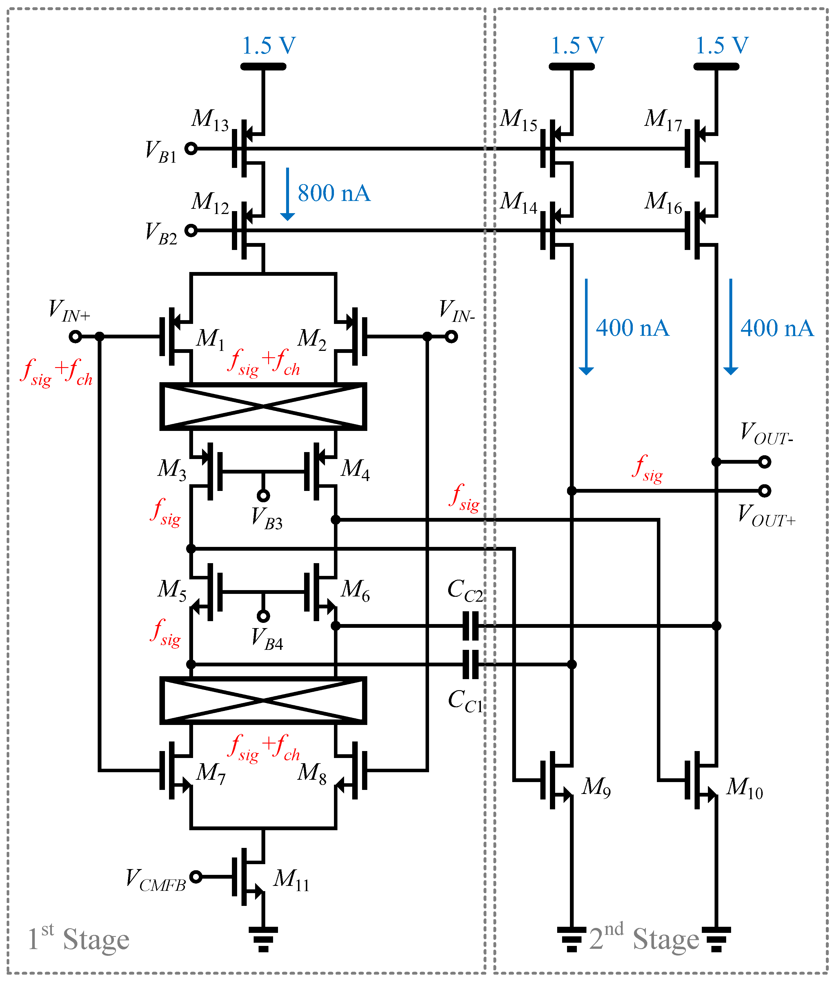
3.1. Architecture of OTA

The OTA adopts a two-stage structure with Ahuja compensation to provide a higher open-loop gain and reduce the closed-loop gain error. The circuit structure of the amplifier is shown in Figure 2.
The first stage adopts the cascode structure with current reuse, which can provide a gain of 84 dB. This design stacks seven transistors between VDD and GND, so the OTA has specific requirements for the voltage headroom. Even though transistors work in the subthreshold region, there are still high demands for supply voltage and voltage distribution. However, a higher supply voltage leads to higher power consumption, which is harmful in the ECG amplifier design. Therefore, the current reuse technique is introduced based on the cascode structure. The equivalent transconductance at a unit current can be doubled by adding an NMOS differential pair to the PMOS differential pair, allowing the same gain to be achieved with less current consumption. In addition, the dual tail current source structure is adopted to improve the PSRR.
We use the common source structure in the second stage to produce a larger output swing. Although the drive capability of this structure is lower than that of the inverter structure, it operates in the Class A state, giving it an advantage. Compared with the inverter structure working in the Class AB state, the common source structure will have better linearity and smaller THD. The second stage uses the cascode current mirror as the load, which may slightly reduce the output swing but will achieve a better PSRR. The output swing remains ample despite the limit of the cascode load, thanks to the higher supply voltage. To stabilize the loop, a frequency compensation capacitor  C C 1 , 2  is added between the input and output of the second stage. However, the traditional Miller compensation generates a zero in the right half plane due to the feedforward effect. The Miller compensation needs to add a zeroing resistance to avoid a zero. In this design, the cascode structure’s characteristics are ingeniously used to connect the Miller compensation capacitor between the drain of  M 9 , 10  and the source of  M 5 , 6  [25]. The isolation effect of  M 5 , 6  allows the feedback current to flow through the capacitor while preventing the feedforward current. This structure avoids the generation of zeroes without additional power consumption.

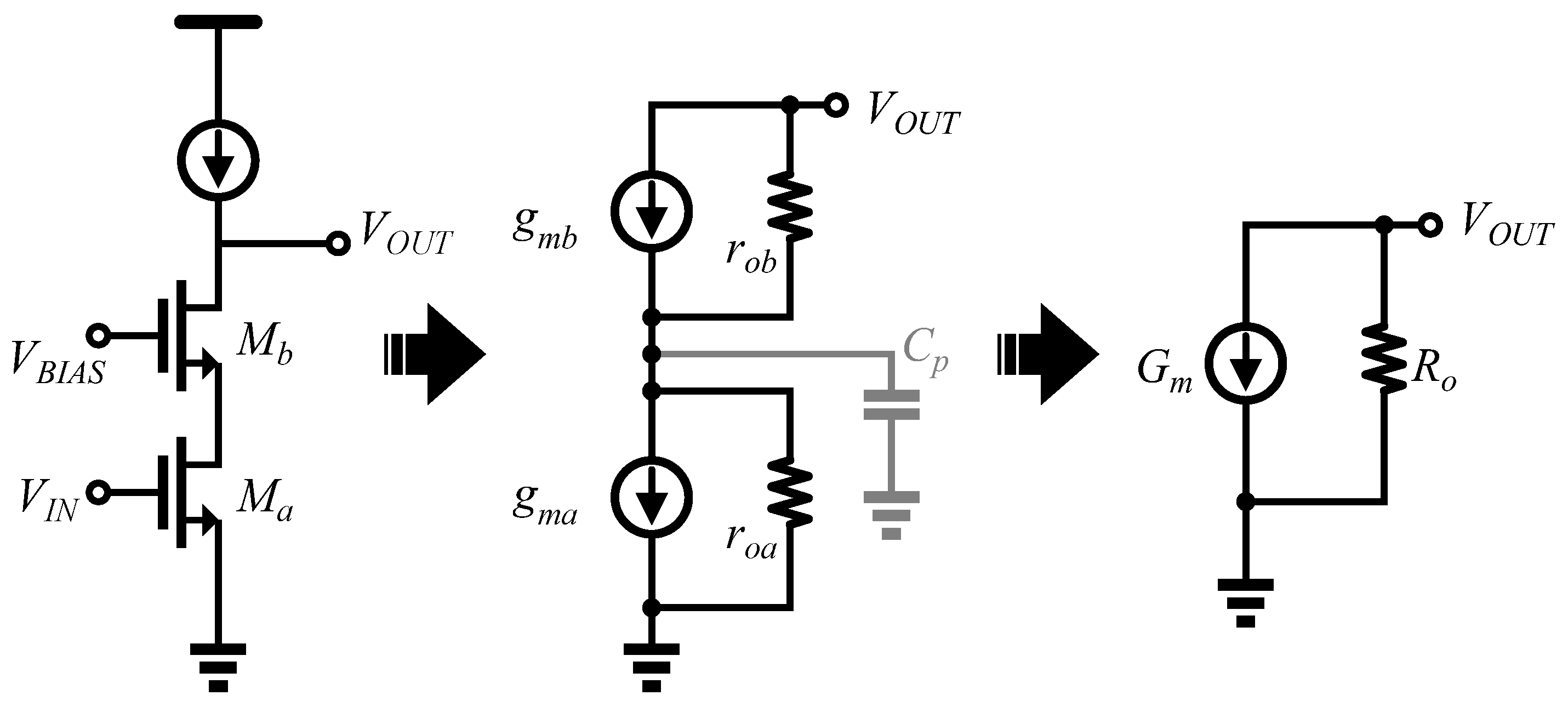
3.2. Analysis of Output Swing

This operational amplifier has a wide input range thanks to the current reuse technique of NMOS and PMOS as input differential pairs. The capacitive-feedback technique ensures that the input common-mode voltage is fixed and the differential mode signal generated by ECG is tiny, making it easy to meet the input range. However, the amplifier has high gain, making the output swing crucial for the large gain to be reflected. In the two-stage OTA, the output stage’s output swing will be the entire amplifier’s bottleneck. The output stage of the proposed amplifier uses a common source structure with the cascode current mirror as a load. A simple analysis of it reveals that
V H i g h = V D D V d s 11 , 12 , 13 V d s 14 , 15 , 16 ,
V L o w = G N D + V g s 9 , 10 .
For high output voltage, in order for the PMOS cascode current mirror to operate in the saturation region, it is necessary to ensure that
V d s 11 , 12 , 13 V d s a t 11 , 12 , 13 ,
V d s 14 , 15 , 16 V d s a t 14 , 15 , 16 .
Therefore, it can be concluded that the maximum output voltage of the output stage is
V H i g h V D D V d s a t 11 , 12 , 13 V d s a t 14 , 15 , 16 .
Similarly, to ensure that input transistor  M 9 , 10  is in the saturation zone when the output voltage is low,  V d s 9 , 10 V d s a t 9 , 10 , so the minimum output voltage is  V L o w V d s a t 9 , 10 . Therefore, the output swing can be expressed as
V s w i n g = V H i g h V L o w V D D V d s a t 11 , 12 , 13 V d s a t 14 , 15 , 16 V d s a t 9 , 10 V D D 3 · V d s a t .
It is feasible to sacrifice some of the output swing to achieve a higher gain using the cascode load, despite leading to a decrease by  V d s . With a 1.5 V supply voltage and around 0.2 V  V d s , a single end can reach an output swing of approximately 0.9 V, while a differential swing can go up to 1.8 V. This output swing is sufficient for ECG signals with smaller amplitudes, even after 60 dB amplification.

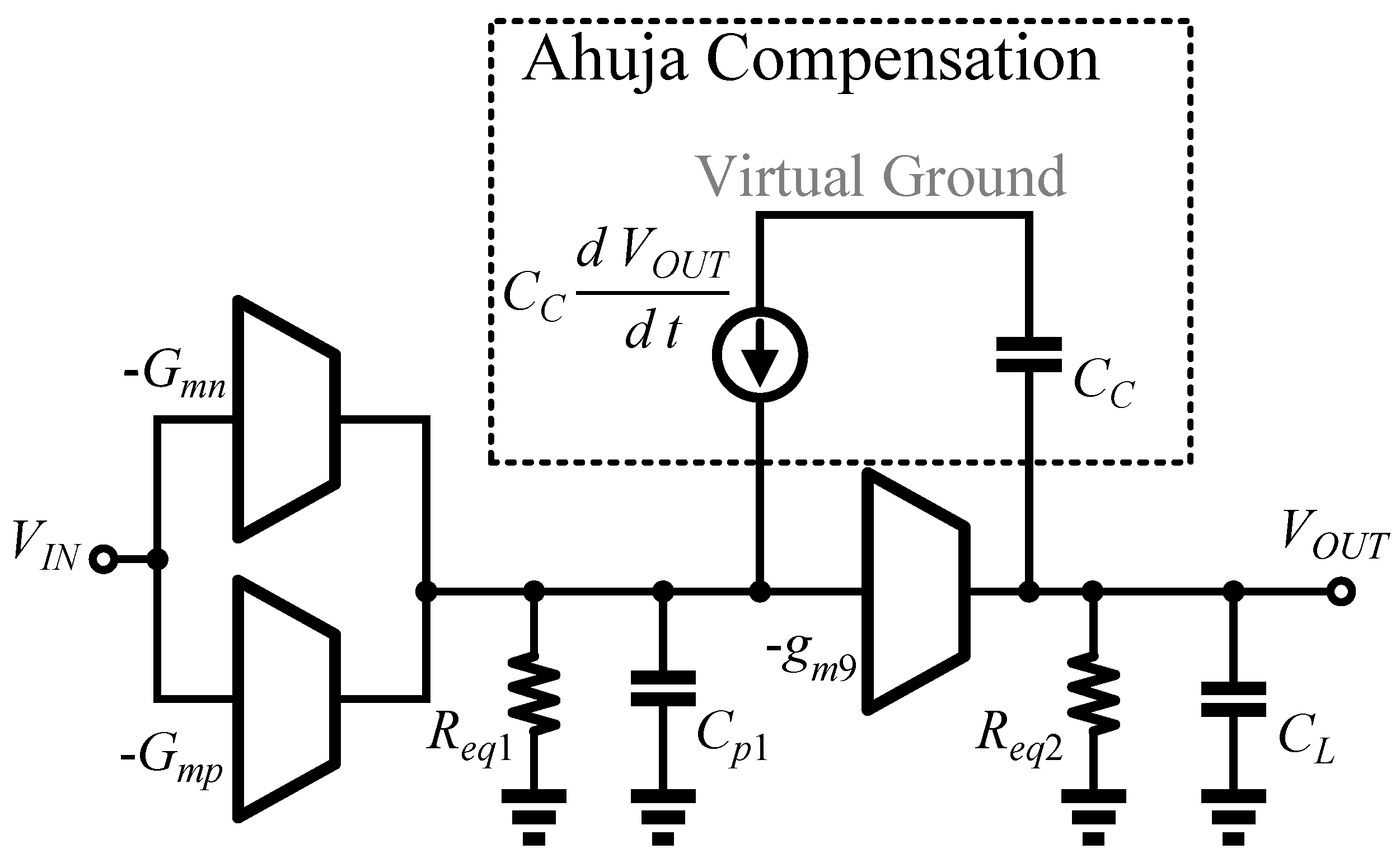
3.3. Analysis of Transfer Function

It is necessary to split and simplify the circuit to obtain a transfer function of OTA simply and intuitively. The proposed OTA structure extensively adopts a cascode structure. Therefore, we analyze the cascode structure first. This structure is shown in Figure 3. We simplify it into a small-signal model as shown in Figure 3, where  g m a  and  r o a  are the transconductance and on-resistance of  M a , and  g m b  and  r o b  are the transconductance and on-resistance of  M b . The equivalent output impedance of this structure is  r o a + r o b + ( g m b + g m b b ) · r o a · r o b , where  g m b b  is the back gate transconductance of  M b . Usually,  ( g m b + g m b ) · r o a · r o b r o a ( g m b + g m b ) · r o a · r o b r o b , and  g m b g m b , so the output impedance of cascode structure  R O  is simplified as  g m b · r o a · r o b . The small signal current generated by the transistor  M a  is diverted to GND by on-resistor  r o a , so the equivalent transconductance  G m  will be slightly smaller than  g m a . To simplify the analysis, an equivalent transconductance  G m  can be approximately equal to  g m a , and this error can be almost negligible.
Considering the frequency response of the cascode structure is essential. Except for the pole at the output, a pole also is generated between the drain of  M a  due to the parasitic capacitance of the transistors, especially the influence of  M b ’s  C g s . However, the capacitance value at this point is minimal, paralleling  C b g s C a g d , and  C a d s , while the resistance is approximately the parallel connection of  1 / g m b  and  r o a . Thus, the pole will be located at high frequencies, far higher than the frequency range of concern in this design, so it can be ignored. The cascode structure can be Norton equivalent to a voltage-controlled current source in parallel with an output resistor as shown in Figure 3, where the values of the equivalent transconductance  G m  and equivalent resistance  R O  are shown in Equations (15) and (16):
G m = g m a .
R O = g m b · r o a · r o b .
Small-signal model of the OTA can be obtained by representing all cascode structures as equivalent transconductance and equivalent output resistance as shown in Figure 4.
In Figure 4 G m n  and  G m p  are the equivalent transconductance of the first-stage NMOS cascode structure and PMOS cascode structure.  R e q 1  is the equivalent output resistance of the first stage, which is the parallel resistance of the NMOS cascode structure’s output impedance  R O N 1  and PMOS cascode structure’s output impedance  R O P 1 C p 1  is a parasitic capacitance at the first stage’s output node, mainly the  C g s 9  of  M 9 . The transconductance of the second-stage input transistor is  g m 9 , and the equivalent output impedance of the second-stage  R e q 2  is on-resistance  r O 9  and output impedance  R O N 2  of the cascode current source in parallel. The frequency compensation capacitor is connected between the input and output of the second stage, and the virtual ground is created by the isolation effect of Ahuja compensation on feedforward. The first-stage DC gain is  A V 1 = ( G m n 1 + G m p 1 ) · R e q 1 , and the second-stage DC gain is  A V 2 = g m 9 · R e q 2 . After simplification, the transfer function can be easily obtained as shown in (17). It can be seen that the OTA has two poles within the concerned frequency range. The secondary pole locates at the output terminal, while the dominant pole is at the first-stage output. The frequency compensation capacitor splits the two poles, ensuring the stability of the OTA [26]:
A V = g m 9 ( G m n + G m p ) R e q 1 R e q 2 α 2 s 2 + α 1 s + 1 ,
where
α 2 = R e q 1 R e q 2 C p 1 ( C L + C C ) ,
α 1 = R e q 1 C p 1 + R e q 2 C L + R e q 2 C C + g m 9 R e q 1 R e q 2 C C .
It should be noted that this analysis does not take into account the gain decrease caused by the chopper. If considering the mixing effect caused by the chopper, the low-frequency gain needs to be multiplied by a coefficient of 2/ π  [27].

3.4. Analysis of Noise
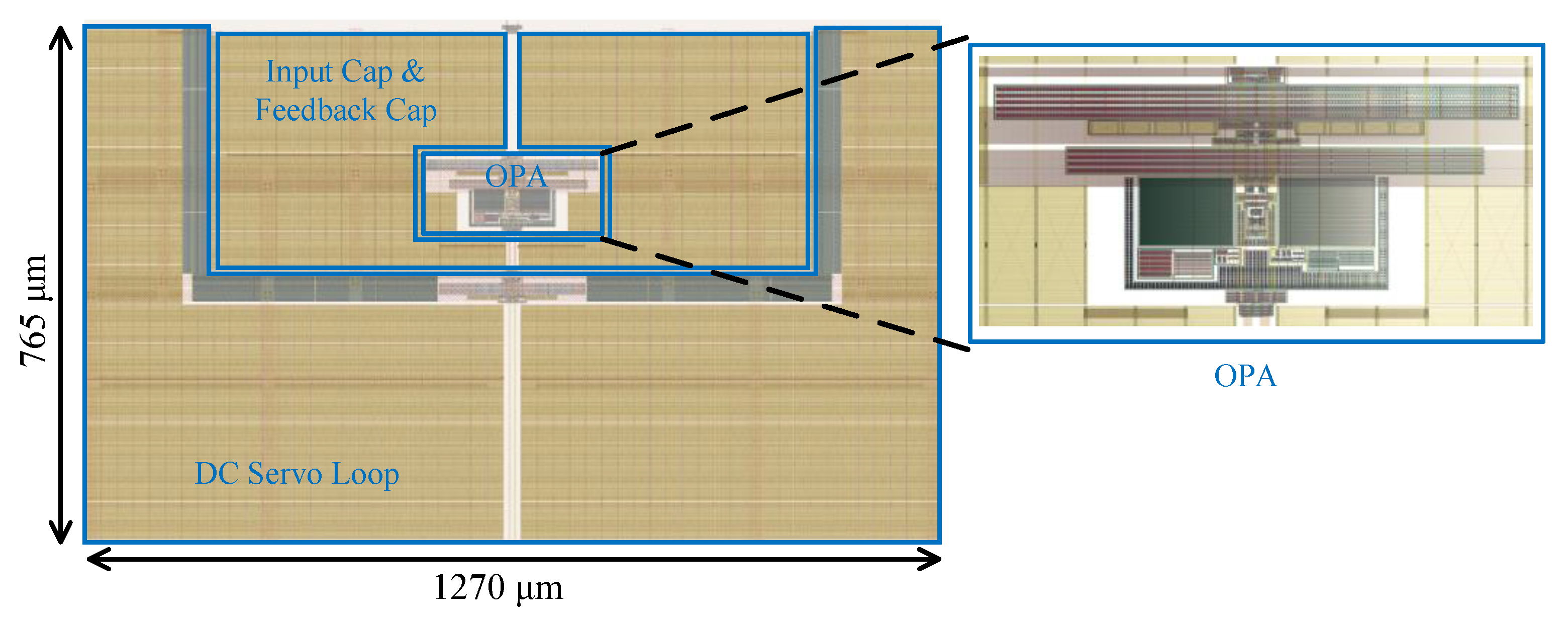
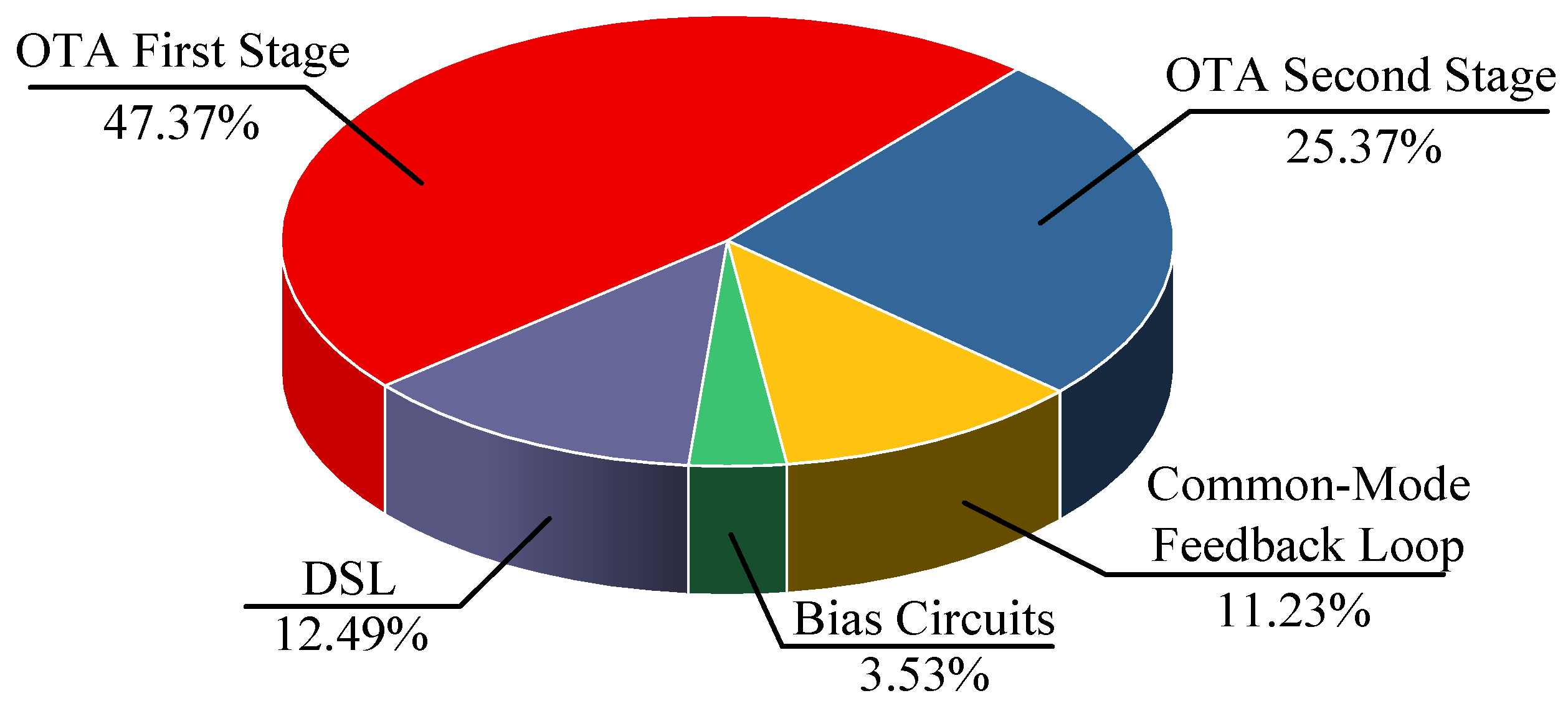
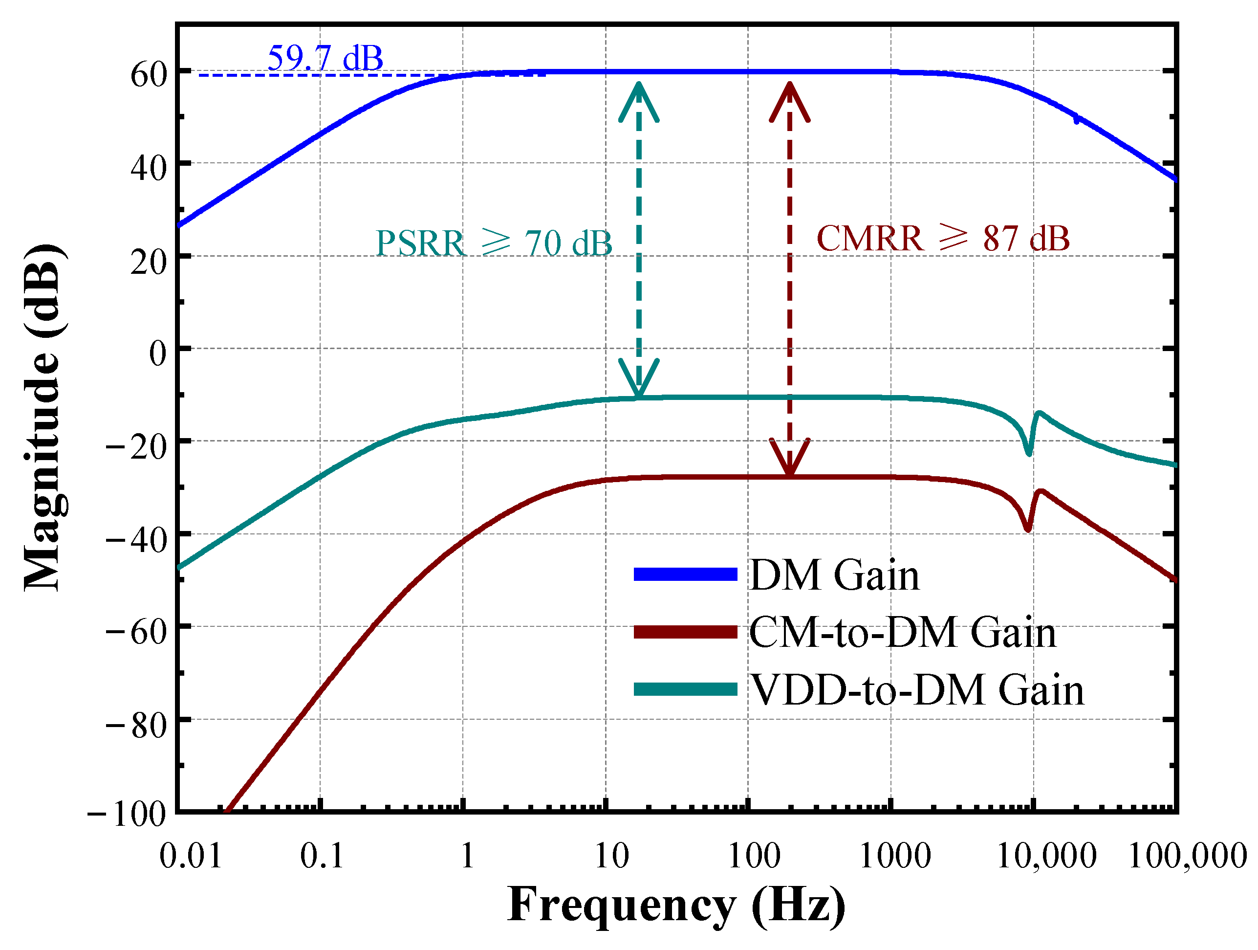
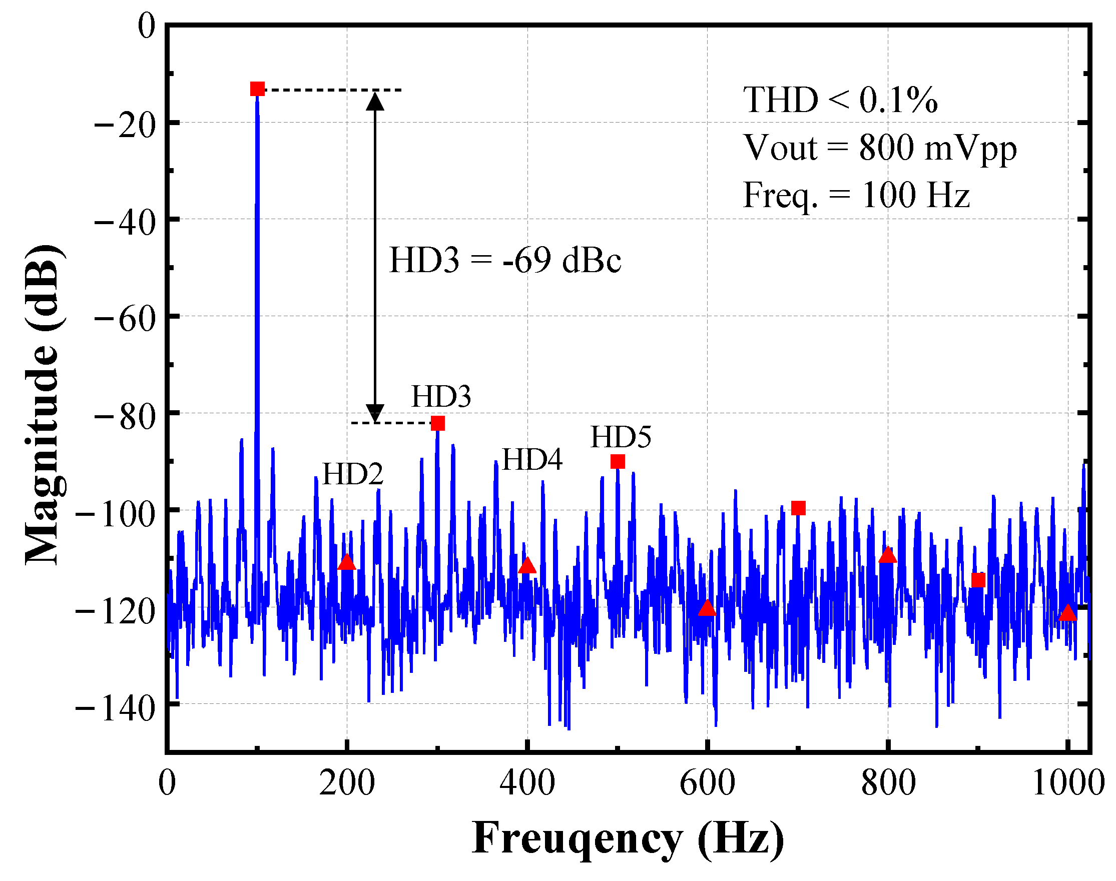
For this particular design, it is essential to consider the noise analysis [28,29]. The ECG recording amplifier’s noise mainly originates from the OTA. All transistors are biased in the subthreshold region in this design to improve the noise-to-power efficiency [30]. The thermal current noise density of MOS transistors that operate in the subthreshold region can be expressed as
i n , t 2 ¯ = 2 k T n g m .
Among them, k is the Boltzmann constant, T is the absolute temperature, n is the subthreshold slope factor, and  g m  is the transconductance of the transistor. In low-frequency applications, in addition to thermal noise, the flicker noise of transistors cannot be ignored, which can be expressed as
i n , f 2 ¯ = g m 2 K C O X W L f
where  g m  is the transconductance of the transistor, K is a process-related constant,  C O X  is the gate-oxide capacitance per unit area, W and L are the channel width and length of the transistor, and f is the frequency. So the noise of each MOSFET includes thermal noise and flicker noise, which can be represented as
i n 2 ¯ = i n , t 2 ¯ + i n , f 2 ¯ = 2 k T n g m + g m 2 K C O X W L f .
In order to achieve low noise, the chopper-stabilized technique can reduce flicker noise at the cost of power consumption and design complexity.
For the first stage of the OTA, thermal noise and flicker noise are equivalent to the input-referred noise voltage:
v n , i n 1 2 ¯ = 2 ( G m n + G m p ) 2 · ( i n 1 , 2 2 ¯ + i n 7 , 8 2 ¯ + i n 3 , 4 2 ¯ g m 3 , 4 2 r O 3 , 4 2 + i n 5 , 6 2 ¯ g m 5 , 6 2 r O 7 , 8 2 ) .
For the second stage of this design, thermal noise and flicker noise are equivalent to the input-referred noise voltage of the first stage:
v n , i n 2 2 ¯ = 2 ( G m n + G m p ) 2 · g m 9 , 10 2 · R e q 1 2 · ( i n 9 , 10 2 ¯ + i n 14 , 16 2 ¯ g m 14 , 16 2 r O 15 , 17 2 ) .
To obtain the total input-referred noise voltage of the OTA, divide the input-referred noise voltage of the second stage by the gain of the first stage. It is important to note that since the first- and second-stages’ noise are unrelated, their noise can be added together directly. Due to the large gain of the first stage, the noise of the second stage equivalent to the OPA input will be very small, even negligible. The total input-referred noise voltage of the OTA can be expressed as
v n , i n 2 ¯ = v n , i n 1 2 ¯ + v n , i n 2 2 ¯ v n , i n 1 2 ¯ = 2 ( G m n + G m p ) 2 · ( i n 1 , 2 2 ¯ + i n 7 , 8 2 ¯ + i n 3 , 4 2 ¯ g m 3 , 4 2 r O 3 , 4 2 + i n 5 , 6 2 ¯ g m 5 , 6 2 r O 7 , 8 2 ) .
In this way, the overall input-referred noise voltage of the proposed OTA is given. It can be seen that the four input transistors of the first stage contribute the most, so the area of these four transistors is increased to further reduce the flicker noise. Considering the suppressive effect of the chopper on the flicker noise of  M 1 , 2 , 7 , 8 , the flicker noise of  M 1 , 2 , 7 , 8  can be ignored, and the total noise can be expressed as
v n , i n 2 ¯ 2 ( G m n + G m p ) 2 · ( 2 k T n g m 1 , 2 + 2 k T n g m 7 , 8 + i n 3 , 4 2 ¯ g m 3 , 4 2 r O 3 , 4 2 + i n 5 , 6 2 ¯ g m 5 , 6 2 r O 7 , 8 2 ) .
The thermal noise of the transistor is closely related to its transconductance. When the overdrive voltage of transistor is kept constant, the transconductance is determined by drain current  I D . Therefore, using the current reuse technique can help reduce the thermal noise of the transistor.
Feedback is provided to the first-stage NMOS tail current source to ensure the output common-mode voltage using a typical continuous time common-mode feedback structure as shown in Figure 5. The resistance detects the common-mode voltage and feedback to the gate of the tail current source through an error amplifier to achieve closed-loop feedback control. Choosing an extremely high resistance value is crucial to prevent the common-mode voltage detection resistor from affecting the gain. However, a large resistor can create a pole with the transistor’s parasitic capacitor. A capacitor can be connected in parallel to generate a zero to counteract the pole. We use the diode-connected NMOS transistors as the load to lower the gain of the error amplifier and maintain the stability of the common-mode feedback loop.

4. Results

We implemented the proposed ECG recording amplifier using the 0.13 μm CMOS process. Figure 6 shows the amplifier’s layout, with an effective area of 0.97 mm2. The input capacitors occupy most of the area.
Based on our simulation results, the proposed amplifier has a total current consumption of 1.647 μA from a 1.5 V supply voltage. The overall power consumption is 2.471 μW. As shown in Figure 7, the current distribution is as follows: the first stage of OTA consumes 780.226 nA, the second stage consumes 417.81 nA, the common-mode feedback loop consumes 184.933 nA, the DSL consumes 205.772 nA, and the bias circuit consumes 58.142 nA.
Figure 8 displays the amplifier’s frequency response, indicating the closed-loop mid-band gain of 59.7 dB and the bandwidth ranging from 0.5 Hz to 6.1 kHz. Additionally, Figure 8 illustrates the common-mode gain and VDD-to-DM gain. The CMRR exceeds 87 dB within bandwidth, while the PSRR exceeds 70 dB.
A 100 Hz single-tone signal is utilized for testing to evaluate the THD performance of the amplifier. The output signal is simulated at 800 mVpp, and a 2048-point DFT is conducted. Figure 9 displays the resulting spectrum. Statistical analysis reveals a THD of 0.07%.
We simulate the noise performance and demonstrate the effect of the chopper-stabilized technique as shown in Figure 10. Without the chopper-stabilized technique, the input-referred noise is 4.8 μVrms integrated from 0.5 Hz to 500 Hz. However, when the chopper-stabilized technique is enabled, the input-referred noise is significantly reduced to 1.18 μVrms. Moreover, the input-referred noise within the entire bandwidth is 3.38 μVrms:
NEF = V I R N , r m s 2 I t o t π · 4 k T V T · B W .
NEF is an essential parameter to measure the amplifiers’ noise and consumption current [31]. The calculation for NEF is provided in Equation (27), wherein  V I R N , r m s  represents the IRN within the bandwidth,  I t o t  denotes the total consumption current, and  B W  stands for the bandwidth. The formula considers k as the Boltzmann constant, T as the absolute temperature, and  V T  as the thermal voltage. The NEF is calculated as 2.13 for this particular design.
We summarize the performance of this design and compare them with relevant designs in recent years as shown in Table 1. Through comparison, we discover that this design has low noise (IRN of 1.18 μVrms and NEF of 2.13) and high linearity (THD of 0.1%).

5. Conclusions

This article presents a new amplifier for ECG recording using a 0.13 μm CMOS process. The amplifier achieves low power, high gain, low noise, and high linearity through chopper-stabilized and current reuse techniques. The amplifier can maintain a large gain by implementing the OTA using the current reuse technique while reducing power consumption. The chopper-stabilized technique achieves low noise and minimizes flicker noise in low-frequency biomedical signals. The fully differential structure is used to suppress odd harmonics. The output stage operates in the Class A state with a higher power supply voltage, resulting in a lower THD when the output signal is large. The simulation results show that the design has advantages, such as high linearity, low power consumption, and low noise. Moreover, thanks to the wider signal bandwidth and larger gain, this design can be used not only for ECG recording but also for other biomedical signal monitoring, such as EEG, EMG, and more.

Author Contributions

Conceptualization, X.C. and P.W.; methodology, B.W. and T.M.; formal analysis, X.C. and T.M.; investigation, P.W.; resources, B.W.; data curation, X.C.; writing—original draft preparation, X.C.; writing—review and editing, T.M.; visualization, X.C.; supervision, B.W.; project administration, X.C. and B.W. All authors have read and agreed to the published version of the manuscript.

Funding

This research received no external funding.

Data Availability Statement

The data in this paper are all from the simulation of real circuits, and there is no data plagiarism or falsification. Due to project confidentiality requirements, we regret that we cannot release more details of the data at this time.

Conflicts of Interest

Author Taishan Mo and Bin Wu was employed by the company Zhejiang Casemic Electronics Technology Co., Ltd. The remaining authors declare that the research was conducted in the absence of any commercial or financial relationships that could be construed as a potential conflict of interest.

References

  1. Lu, S.; Yang, J.; Yang, B.; Yin, Z.; Liu, M.; Yin, L.; Zheng, W. Analysis and Design of Surgical Instrument Localization Algorithm. CMES-Comput. Model. Eng. Sci. 2023, 137, 669–685. [Google Scholar] [CrossRef]
  2. Tang, T.; Goh, W.L.; Yao, L.; Cheong, J.H.; Gao, Y. An integrated multi-channel biopotential recording analog front-end IC with area-efficient driven-right-leg circuit. IEEE Trans. Biomed. Circuits Syst. 2019, 14, 297–304. [Google Scholar] [CrossRef]
  3. Wang, W.; Qi, F.; Wipf, D.; Cai, C.; Yu, T.; Li, Y.; Yu, Z.; Wu, W. Sparse bayesian learning for end-to-end EEG decoding. IEEE Trans. Pattern Anal. Mach. Intell. 2023, 45, 15632–15649. [Google Scholar] [CrossRef]
  4. Wang, C.; Zhang, X.; Liu, Y.; Li, J.; Zhu, L.; Lu, Y.; Guo, X.; Chen, D. An enzyme-particle hybrid ink for one step screen-printing and long-term metabolism monitoring. Anal. Chim. Acta 2022, 1221, 340168. [Google Scholar] [CrossRef]
  5. Bing, P.; Liu, Y.; Liu, W.; Zhou, J.; Zhu, L. Electrocardiogram classification using TSST-based spectrogram and ConViT. Front. Cardiovasc. Med. 2022, 9, 983543. [Google Scholar] [CrossRef] [PubMed]
  6. Tian, Y.; Qin, Z.; Yu, Y.; Gao, D.; Liao, X.; Liu, L. A Low-Noise and Low-Power Multi-Channel ECG AFE Based on Orthogonal Current-Reuse Amplifier. IEEE Trans. Circuits Syst. I Regul. Pap. 2023, 70, 3167–3177. [Google Scholar] [CrossRef]
  7. Dang, W.; Xiang, L.; Liu, S.; Yang, B.; Liu, M.; Yin, Z.; Yin, L.; Zheng, W. A Feature Matching Method based on the Convolutional Neural Network. J. Imaging Sci. Technol. 2023, 67. [Google Scholar] [CrossRef]
  8. Johnson, B.; Molnar, A. An orthogonal current-reuse amplifier for multi-channel sensing. IEEE J. Solid-State Circuits 2013, 48, 1487–1496. [Google Scholar] [CrossRef]
  9. Winter, B.B.; Webster, J.G. Driven-right-leg circuit design. IEEE Trans. Biomed. Eng. 1983, BME-30, 62–66. [Google Scholar] [CrossRef]
  10. Hu, H.; Lin, C.C.; Gupta, S. A 197.1-μW Wireless Sensor SoC with an Energy-Efficient Analog Front-End and a Harmonic Injection-Locked OOK TX. IEEE Trans. Circuits Syst. I Regul. Pap. 2021, 68, 2444–2456. [Google Scholar] [CrossRef]
  11. Zhang, J.; Zhang, H.; Sun, Q.; Zhang, R. A low-noise, low-power amplifier with current-reused OTA for ECG recordings. IEEE Trans. Biomed. Circuits Syst. 2018, 12, 700–708. [Google Scholar] [CrossRef] [PubMed]
  12. Mondal, S.; Hall, D.A. A 13.9-nA ECG amplifier achieving 0.86/0.99 NEF/PEF using AC-coupled OTA-stacking. IEEE J. Solid-State Circuits 2019, 55, 414–425. [Google Scholar] [CrossRef]
  13. Li, Q.; Wang, X.; Liu, Y. A 60 nV/Hz <0.01%-THD ±200 mV-DC-Rejection Bio-Sensing Chopper Amplifier With Noise-Nonlinearity-Cancelling Loop. IEEE Trans. Circuits Syst. II Express Briefs 2019, 67, 215–219. [Google Scholar]
  14. Song, S.; Rooijakkers, M.; Harpe, P.; Rabotti, C.; Mischi, M.; van Roermund, A.H.; Cantatore, E. A low-voltage chopper-stabilized amplifier for fetal ECG monitoring with a 1.41 power efficiency factor. IEEE Trans. Biomed. Circuits Syst. 2015, 9, 237–247. [Google Scholar] [CrossRef] [PubMed]
  15. Wang, T.Y.; Lai, M.R.; Twigg, C.M.; Peng, S.Y. A fully reconfigurable low-noise biopotential sensing amplifier with 1.96 noise efficiency factor. IEEE Trans. Biomed. Circuits Syst. 2013, 8, 411–422. [Google Scholar] [CrossRef] [PubMed]
  16. Tang, T.; Goh, W.L.; Yao, L.; Gao, Y. A TDM-based 16-channel AFE ASIC with enhanced system-level CMRR for wearable EEG recording with dry electrodes. IEEE Trans. Biomed. Circuits Syst. 2020, 14, 516–524. [Google Scholar] [CrossRef]
  17. Huang, X.; Ballini, M.; Wang, S.; Miccoli, B.; Van Hoof, C.; Gielen, G.; Craninckx, J.; Van Helleputte, N.; Lopez, C.M. A compact, low-power analog front-end with event-driven input biasing for high-density neural recording in 22-nm FDSOI. IEEE Trans. Circuits Syst. II Express Briefs 2021, 69, 804–808. [Google Scholar] [CrossRef]
  18. Ha, U.; Lee, J.; Kim, M.; Roh, T.; Choi, S.; Yoo, H.J. An EEG-NIRS multimodal SoC for accurate anesthesia depth monitoring. IEEE J. Solid-State Circuits 2018, 53, 1830–1843. [Google Scholar] [CrossRef]
  19. Zhang, T.; Li, Y.; Su, C.; Zhang, X.; Yang, Y. A 1V 3.5 μW Bio-AFE with Chopper-Capacitor-Chopper Integrator-Based DSL and Low Power GM-C Filter. IEEE Trans. Circuits Syst. II Express Briefs 2021, 69, 5–9. [Google Scholar]
  20. Samiei, A.; Hashemi, H. A chopper stabilized, current feedback, neural recording amplifier. IEEE Solid-State Circuits Letters 2019, 2, 17–20. [Google Scholar] [CrossRef]
  21. Lee, C.J.; Song, J.I. A chopper-stabilized amplifier with a tunable bandwidth for EEG acquisition applications. IEEE Access 2019, 7, 73165–73171. [Google Scholar] [CrossRef]
  22. Martins, R.; Selberherr, S.; Vaz, F.A. A CMOS IC for portable EEG acquisition systems. IEEE Trans. Instrum. Meas. 1998, 47, 1191–1196. [Google Scholar] [CrossRef]
  23. Hoseini, Z.; Nazari, M.; Lee, K.S.; Chung, H. Current feedback instrumentation amplifier with built-in differential electrode offset cancellation loop for ECG/EEG sensing frontend. IEEE Trans. Instrum. Meas. 2020, 70, 1–11. [Google Scholar] [CrossRef]
  24. Miaofen, L.; Youmin, L.; Tianyang, W.; Fulei, C.; Zhike, P. Adaptive synchronous demodulation transform with application to analyzing multicomponent signals for machinery fault diagnostics. Mech. Syst. Signal Process. 2023, 191, 110208. [Google Scholar] [CrossRef]
  25. Ng, K.A.; Xu, Y.P. A low-power, high CMRR neural amplifier system employing CMOS inverter-based OTAs with CMFB through supply rails. IEEE J. Solid-State Circuits 2016, 51, 724–737. [Google Scholar]
  26. Wang, Y.; Chen, P.; Yong, J.; Xu, W.; Xu, S.; Liu, K. A comprehensive investigation on the selection of high-pass harmonic filters. IEEE Trans. Power Deliv. 2022, 37, 4212–4226. [Google Scholar] [CrossRef]
  27. Enz, C.C.; Vittoz, E.A.; Krummenacher, F. A CMOS chopper amplifier. IEEE J. Solid-State Circuits 1987, 22, 335–342. [Google Scholar] [CrossRef]
  28. Hu, J.; Wu, Y.; Li, T.; Ghosh, B.K. Consensus control of general linear multiagent systems with antagonistic interactions and communication noises. IEEE Trans. Autom. Control 2018, 64, 2122–2127. [Google Scholar] [CrossRef]
  29. Li, M.; Wang, T.; Chu, F.; Han, Q.; Qin, Z.; Zuo, M.J. Scaling-basis chirplet transform. IEEE Trans. Ind. Electron. 2020, 68, 8777–8788. [Google Scholar] [CrossRef]
  30. Enz, C.C.; Krummenacher, F.; Vittoz, E.A. An analytical MOS transistor model valid in all regions of operation and dedicated to low-voltage and low-current applications. Analog. Integr. Circuits Signal Process. 1995, 8, 83–114. [Google Scholar] [CrossRef]
  31. Chen, F.; Chandrakasan, A.P.; Stojanovic, V.M. Design and analysis of a hardware-efficient compressed sensing architecture for data compression in wireless sensors. IEEE J. Solid-State Circuits 2012, 47, 744–756. [Google Scholar] [CrossRef]
  32. Sawigun, C.; Thanapitak, S. A Compact Sub-μW CMOS ECG Amplifier With 57.5-MΩ Zin, 2.02 NEF, 8.16 PEF and 83.24-dB CMRR. IEEE Trans. Biomed. Circuits Syst. 2021, 15, 549–558. [Google Scholar] [CrossRef] [PubMed]
  33. Zhou, Z. A front-end amplifier with current compensation feedback input impedance booster for neural signal applications. IEEE Access 2020, 8, 178055–178062. [Google Scholar] [CrossRef]
  34. Pham, X.T.; Nguyen, N.T.; Nguyen, V.N.; Lee, J.W. Area and power-efficient capacitively-coupled chopper instrumentation amplifiers in 28 nm CMOS for multi-channel biosensing applications. IEEE Access 2021, 9, 86773–86785. [Google Scholar] [CrossRef]
Figure 1. The system structure of the proposed amplifier.
Electronics 13 00378 g001
Figure 2. The core circuit structure of the OTA.
Electronics 13 00378 g002
Figure 3. Analysis and simplification of cascode structure.
Electronics 13 00378 g003
Figure 4. The small-signal model of the OTA.
Electronics 13 00378 g004
Figure 5. Circuit structure of the error amplifier in the common-mode feedback loop.
Electronics 13 00378 g005
Figure 6. Layout of the amplifier.
Electronics 13 00378 g006
Figure 7. Power consumption distribution for the amplifier.
Electronics 13 00378 g007
Figure 8. Simulation of the frequency response.
Electronics 13 00378 g008
Figure 9. Frequency spectrum for a 100 Hz input sinusoid signal.
Electronics 13 00378 g009
Figure 10. Simulation of input-referred noise.
Electronics 13 00378 g010
Table 1. Performance comparison with the states of the art.
[11]
TBCAS’18
[13]
TCS II’19
[20]
SSCL’19 a
[32]
TBCAS’21
[33]
ACCESS’20
[34]
ACCESS’21
This Work b
Technology0.35 μm0.18 μm0.18 μm0.35 μm0.18 μm28 nm0.13 μm
Area (mm2)0.180.460.080.0710.0250.050.97
Voltage (V)21.20.6, 1.221.811.5
Current (A)160 n2 μN.A.0.336 μN.A.1 μ1.647 μ
Power (W)320 n2.4 μ2.6 μ0.672 μ7.6 μ1 μ2.471 μ
Gain (dB)39.84041–5940.61439.559.7
Bandwidth (Hz)0.2–2000.5–5002007.84m-3000.01–23 k1 k0.5-6.1 k
Input-Referred
Noise (μVrms)
2.05
(0.1–10 kHz)
1.8
(0.5–500 Hz)
3.21.54
(0.1–300 Hz)
N.A.2.74
(1–200 Hz)
1.18
(0.5–500 Hz)
THD<1%
20 Hz
15 mVpp
Input
0.01%
69 Hz
800 mVp
Output
1.7%
1 kHz
1 mVpp
Input
0.12%
100 Hz
5 mVp
Input
−49 db
1 kHz
1 mVpp
Input
−52.6 dB
100 Hz
1.5 mVp
Input
<0.1%
100 Hz
800 mVpp
Output
CMRR (dB)>65>907083.246194≥87
PSRR (dB)>70N.A.N.A.84.25779≥70
NEF2.264.43.22.024.7 c7.52.13
a Represents the results of the neural amplifier for the action potential. b Represents the simulation results. c Represents NEF of the neural amplifier for the action potential.
Disclaimer/Publisher’s Note: The statements, opinions and data contained in all publications are solely those of the individual author(s) and contributor(s) and not of MDPI and/or the editor(s). MDPI and/or the editor(s) disclaim responsibility for any injury to people or property resulting from any ideas, methods, instructions or products referred to in the content.

