Article

A Bidirectional Simultaneous Wireless Power and Data Transfer System with Non-Contact Slip Ring

by
Yuanshuang Fan
1,
Qiurui Chen
1,*,
Sihan Wu
1,
Jing Xiao
2 and
Zhihui Wang
1
1
College of Automation, Chongqing University, Chongqing 400044, China
2
Southern Power Grid Corporation Wireless Power Transmission Joint Laboratory, Guangxi Power Grid Company Ltd., Nanning 530023, China
*
Author to whom correspondence should be addressed.
Electronics 2024, 13(20), 3974; https://doi.org/10.3390/electronics13203974 (registering DOI)
Submission received: 2 September 2024 / Revised: 29 September 2024 / Accepted: 4 October 2024 / Published: 10 October 2024
(This article belongs to the Section Microwave and Wireless Communications)

Abstract

:
A non-contact slip ring is proposed in this paper. The bidirectional simultaneous wireless power and data transfer (BD-SWPDT) technology is utilized to transfer power and data bidirectionally. A bidirectional constant-voltage LC hybrid compensation topology is proposed, which utilizes the LC series parallel structure to have different equivalent models at different frequencies. By using different operating frequencies for forward and reverse power transfer, the system’s forward and reverse transfer can be equivalent to different constant-voltage output compensation topologies. The resonant parameters of the system are designed to achieve consistent voltage gain for forward and reverse power transfer. And based on this topology, a data carrier injection method is designed to achieve high Signal Noise Ratio (SNR) simultaneous data transfer. To improve the flexibility of non-contact slip ring installation, a caliper-type coupling structure is proposed. Finally, the feasibility of the proposed method is verified through experiments, achieving a forward and reverse output power of 200 W and half duplex communication with a data rate of 19.2 kbps.

1. Introduction

Magnetic Coupled Wireless Power Transfer (MC-WPT) technology is based on the principle of electromagnetic induction, which achieves the transmission of electrical power through non-contact means, directly avoiding physical contact between rotating structures and providing an effective means for the development of electrical power transmission technology for rotating structures [1,2]. With the development of WPT technology, it has been applied in multiple fields, such as smart homes, mobile phones, electric vehicles, and medical devices [3,4,5,6,7,8]. In addition, it has gradually been applied in some special industries, such as wireless power supply in underwater environments [9,10] and rotary guidance systems in the field of oil drilling [11].
In recent years, rotating equipment has gradually been applied in various fields of our lives, especially in some very important areas, such as satellites, helicopters, radars, oil drilling, and wind power generation [12]. During the operation of the equipment, it is necessary to transmit the electrical power from the stator side to the rotor side, and at the same time, the sensor signals on the rotor side also need to be transmitted back to the host for internal operation and control. Due to the need for the device to rotate 360°, in order to prevent cable entanglement, the internal power transmission of the rotating structure is usually achieved through conductive slip rings. For the wireless power transfer of rotary structures, wireless power transfer technology with rotary structures has been widely studied. A wireless power transfer rotary structure for a solar wing is proposed in [12], a multi-U-shaped column rotary transformer is proposed in [13], and a mixed flux coupler is proposed in [14]. The couplers adopted in these papers are traditional coaxial nested slip rings. However, the flexibility of this type of coupler is not high, and only unidirectional power transfer is achieved without simultaneous data transfer. End-to-end couplers are also proposed in [15,16,17,18] and Series or None compensation is adopted in these papers, which will cause serious interference to data transfer when data are simultaneously transferred sharing the same coupler [19]. In practical applications, in addition to power transfer, simultaneous wireless data transfer is also needed. A simultaneous wireless power and data transfer method adopting a half-cylinder stator and quarter-cylinder rotator coupler is proposed in [20], which achieves simultaneous data transfer while supplying power to rotating equipment. However, extra coils for data transfer are added in the coupler, which will reduce the flexibility of the coupler. In some rotating applications, such as a satellite solar wing, batteries are usually stored inside the satellite; when there is sunlight, solar panels absorb solar radiation and convert it into electrical energy to power devices such as sail sensors. At the same time, the electrical energy is transmitted to the satellite’s internal battery for storage through conductive slip rings. While the satellite operates in the shadow of the sun, the electrical energy in the battery is released to provide power for the equipment. The sensor devices on the solar panel need to be powered through conductive slip rings. In the process of power transfer, it is also necessary to transmit control data to control the operation of sensors and other equipment on solar panels, and to transmit sensor data through slip rings to the satellite for processing. These demands can be exactly met by a BD-SWPDT system.
A bidirectional simultaneous wireless power and data transfer (BD-SWPDT) system with non-contact slip ring based on caliper type coupling structure is proposed in this paper. A bidirectional constant-voltage LC hybrid compensation topology and a BD-SWPDT topology are proposed, and a caliper-type coupler is designed to improve system flexibility. In the power transfer channel, based on the capacitive or inductive characteristics of LC series and parallel networks at different frequencies, by controlling the frequency during bidirectional power transfer, the system topology is equivalent to different constant-voltage output topologies in forward and reverse power transfer, achieving constant voltage output during bidirectional power transfer. For data transfer, amplitude shift keying (ASK) is adopted, the coupler is frequency division multiplexed, and parallel networks with a center frequency of the data carrier to achieve the impedance isolation of the power and data transfer channel are added. Finally, bidirectional simultaneous wireless power and data transfer is achieved through the same caliper-type coupling structure. The proposed system has the following features:
(1)
Simultaneous wireless power and data transfer through a pair of coupled coils;
(2)
An on-contact slip ring based on a caliper-type coupling structure is utilized to replace the traditional contact slip ring equivalently;
(3)
Bidirectional power transfer with independent transfer gains is achieved;
(4)
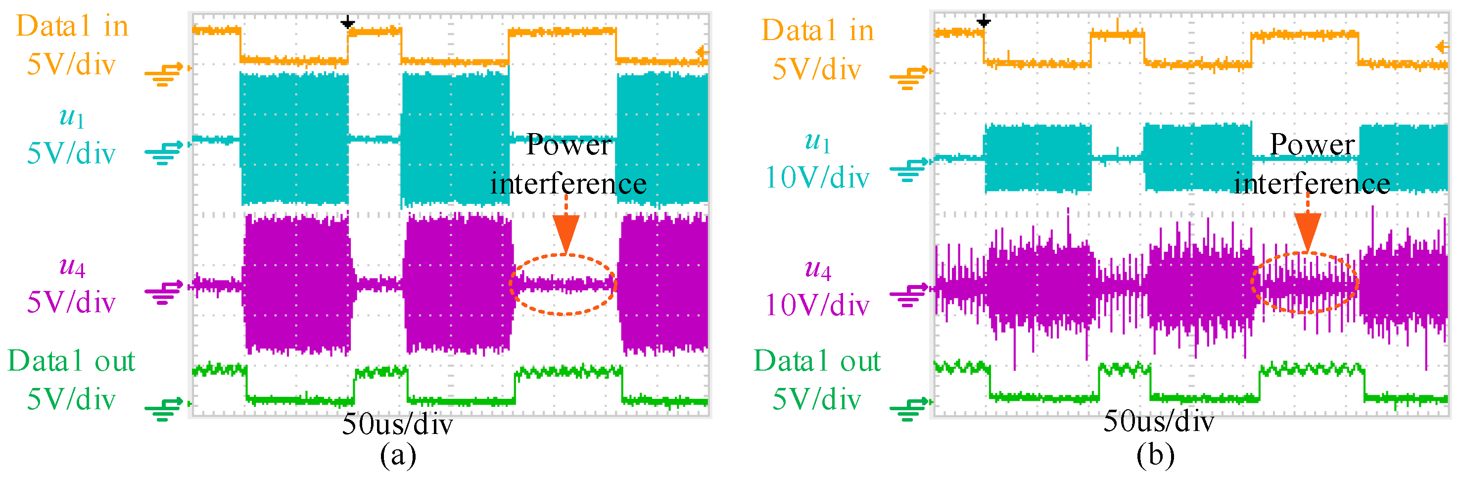
A constant-voltage output topology with band-pass filtering characteristics is proposed, achieving constant voltage output and suppressing the power interference on simultaneous data transfer.
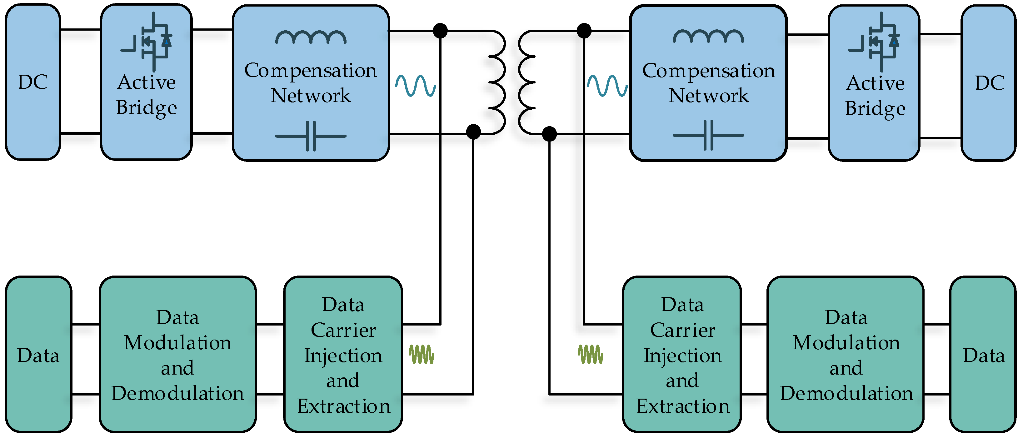
This paper is organized as follows. In Section 2, a structural diagram of the BD-SWPDT system is shown. In Section 3, the bidirectional power transfer channel is analyzed based on its circuit models, and its operation principle is illustrated. In addition, the caliper-type coupler is analyzed through simulation. In Section 4, the structure of the simultaneous data transfer channel is proposed, and its operation principle is illustrated. In Section 5, an experimental prototype is built to verify the correctness of the theoretical analysis and the feasibility of the proposed system. In Section 6, a discussion is offered, and the results of the proposed system are compared with the references. Finally, a conclusion is drawn in Section 7.

2. System Overview

The structural diagram of the proposed BD-SWPDT is shown in Figure 1. The power transfer channel and the data transfer channel share the same pair of coupled coils. In the power transfer channel, when electrical power flows in the forward direction, a driving signal is applied on the primary active bridge and the active bridge operates in an inverter mode to generate high-frequency voltage. The reactive power of the system is compensated by a compensation network, and an alternating magnetic field is generated on the primary coil. The reactive power of the system is also compensated by a compensation network on the secondary side. The secondary active bridge is not applied on a driving signal, or operates in a rectification mode using a control strategy to convert AC into DC, thereby achieving the forward transmission of electrical power. Similarly, when electrical energy flows in the opposite direction, a secondary side active bridge is applied on a driving signal and operates in inverter mode, while the primary side is in rectification mode. The system achieves bidirectional power transfer by controlling the driving signals of the primary and secondary sides. In the data transfer channel, when data are forward-transferred, the data are modulated onto a high-frequency carrier through a modulation module, and the high-frequency carrier is injected into the primary coils through the data carrier injection module. On the secondary side, the carrier is extracted by the data carrier extraction module and demodulated by the data demodulation module to recover the data. Due to the symmetric structure of the data transfer channel, the process of reverse data transfer is the same as forward data transfer.

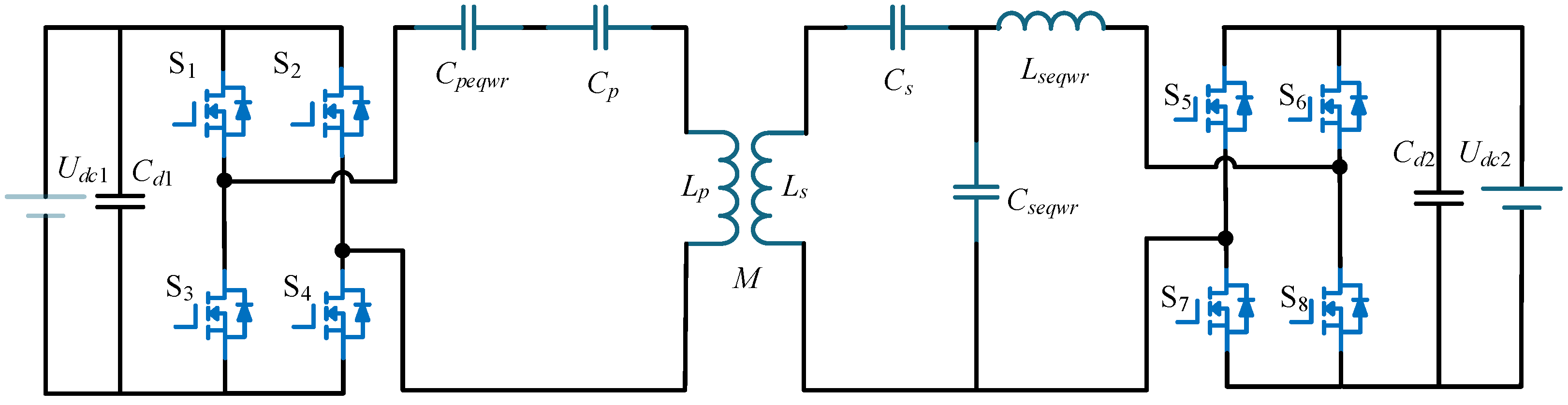
3. Bidirectional Power Transfer Channel

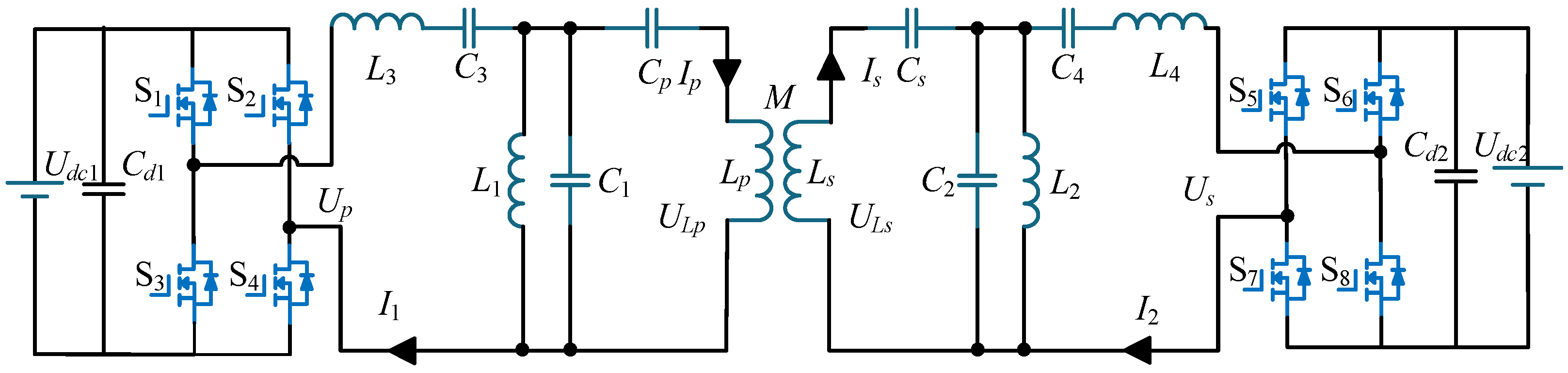
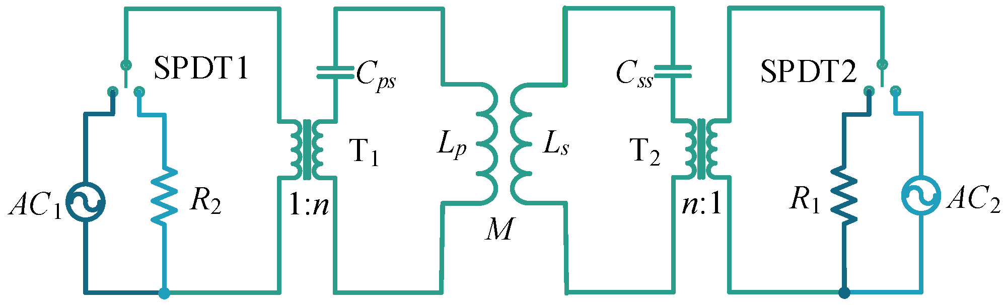
3.1. The Topology of the Power Transfer Channel

When power and data are transferred simultaneously via the same pair of coupled coils, the data transfer channel will be greatly interfered with by the harmonics components of the power transfer channel. To suppress the interference of the power transfer channel, compensation topologies with band-pass filtering characteristics such as LCC compensation topology are usually adopted in both sides of an SWPDT system [19]. A bidirectional constant voltage LC hybrid compensation topology is proposed in the paper, as shown in Figure 2. Based on the capacitive or inductive characteristics of LC series in parallel networks at different frequencies, the system topology is equivalent to different constant-voltage output topologies in the forward and reverse transmission processes, controlling the frequency during the bidirectional transmission of electrical power, and achieving constant-voltage output in the bidirectional transmission process. Udc1 and Udc2 are equivalent DC power sources for forward and reverse power transfer. Lp and Ls are the self-inductance of the primary and secondary coils, M is the mutual inductance of the coupled coils, Ip and Is are the current of the primary and secondary side coils, ULp and ULs are the voltages of the primary and secondary side coils, Up and I1 are the voltage and current of the primary side inverter, Us and I2 are the voltage and current of the secondary side inverter, and Cd1 and Cd2 are the input or output filtering capacitors. S1–S4 and S5–S8 represent the active bridges composed of four MOSFETs on the primary and secondary sides, respectively, and they are used to achieve DC inversion and controllable rectification in the bidirectional power transfer. LC hybrid compensation topologies are adopted on the primary and secondary sides of the system.
The forward and reverse power transfer adopts different operating frequencies. In this paper, the operating frequency of the forward power transfer is ff, the operating frequency of the reverse power transfer is fr, and ff < fr; the forward and reverse operating angular frequencies are ωf and ωr, respectively. The resonant frequency of the LC parallel network composed of L1 and C1 is ω1, the resonant frequency of the parallel network composed of L2 and C2 is ω2, the resonant frequency of the series LC network composed of L3 and C3 is ω3, and the resonant frequency of the series LC network composed of L4 and C4 is ω4. The relationships between each parameter in Figure 2 satisfy
ω 4 < ω 2 = ω f < ω r = ω 1 < ω 3 ω 1 = ω r = 2 π f r = 1 / L 1 C 1 ω 2 = ω f = 2 π f f = 1 / L 2 C 2 ω 3 = 1 / L 3 C 3 ω 4 = 1 / L 4 C 4
Due to ω2 = ωf, when power is transmitted in the forward direction, the impedance of the parallel network composed of L2 and C2 on the secondary side is infinite, equivalent to an open circuit. The secondary side is equivalent to a series compensation network. At the forward operating frequency, the series LC network composed of L3 and C3 is capacitive, while the LC parallel network composed of L1 and C1 is inductive. The forward power transfer topology structure can be equivalent to a CLC-S topology with a constant-voltage output characteristic.
When power is transmitted in the forward direction (the operating frequency is ff), the equivalent capacitance of the series network (i.e., L3, C3) Cpeqwf can be derived, as
C p e q w f = C 3 1 ω f 2 L 3 C 3
The equivalent inductance of the parallel network (i.e., L1, C1) Leqwf can be derived as
L p e q w f = L 1 1 ω f 2 L 1 C 1
The primary compensation topology structure for power transfer can be equivalent to a CLC compensation topology composed of Cpeqwf, Lpeqwf, and Cp. The parallel network is equivalent to an open circuit. The series network (i.e., L4, C4) is equivalent to an inductor Lseqwf.
L s e q w f = L 4 1 ω f 2 C 4
The equivalent circuit diagram of the forward power transfer channel is shown in Figure 3.
When power is transferred in the forward direction, the secondary side active bridge operates in rectification mode, and the inverter can be treated as a voltage source Up and the load, while the rectifier is equivalent to a resistor Rseq. Based on First Harmonic Approximation (FHA), U p = 2 2 U d c 1 π . The further equivalent circuit of the forward power transfer channel is shown in Figure 4.
The relationship between each parameter satisfies
j ω f L p e q w f + 1 j ω f C p e q w f = 0 j ω f L p + L p e q w f + 1 j ω f C p = 0 j ω f L s + L s e q w f + 1 j ω f C s = 0
Based on (2), (3), and (5), The output current of the primary inverter can be derived as
I ˙ 1 = 2 2 M 2 ( 1 ω f 2 L 1 C 1 ) 2 U d c 1 π R s e q L 1 2
and the current of the primary coil can be obtained.
I ˙ p = 2 2 U d c 1 ( ω f 2 L 1 C 1 1 ) j ω f L 1 π
The voltage transfer gain of the forward power transfer channel can be expressed as
G f = U d c 2 U d c 1 = M L p e q w f = M ( 1 ω f 2 L 1 C 1 ) L 1
When power is transmitted in reverse, due to ω1 = ωr, the parallel network composed of L1 and C1 on the primary side is equivalent to an open circuit, the series LC network composed of L4 and C4 on the secondary side is inductive, and the parallel network composed of L2 and C2 is capacitive. The reverse power transfer topology structure can be equivalent to the LCC-S topology, and the system can achieve constant voltage output.
When power is transmitted in the reverse direction (the operating frequency is fr), the equivalent inductance of the series network (i.e., L4, C4) Lseqwr can be derived,
L s e q w r = L 4 1 ω r 2 C 4
The equivalent capacitance of the parallel network (i.e., L2, C2) Ceqwr can be derived as
C s e q w r = C 2 1 ω r 2 L 2
The secondary compensation topology structure for reverse power transfer can be equivalent to an LCC compensation topology composed of Lseqwr, Cseqwr, and Cs. The parallel network is equivalent to an open circuit. The series network (i.e., L3, C3) is equivalent to a capacitor Cpeqwr.
C p e q w r = C 3 1 ω r 2 L 3 C 3
The equivalent circuit diagram of the reverse power transfer channel is shown in Figure 5.
The relationship between each parameter satisfies
j ω r L s e q w r + 1 j ω r C s e q w r = 0 j ω r L s L s e q w r + 1 j ω r C s = 0 j ω r L p + 1 j ω r C p e q w r + 1 j ω r C p = 0
Similar to the forward power transfer, the voltage transfer gain of the reverse power transfer channel can be expressed as
G r = U d c 1 U d c 2 = M L s e q w r = ω r 2 C 4 M ω r 2 L 4 C 4 1
According to the voltage gain formula of the forward and reverse power transfer, when the input voltage of the system is constant, the magnitude of the output voltage is related to the value of the equivalent inductance (Lpeqwf or Lseqwr) and M, and is independent of the load, which can enable it to achieve constant voltage output. In addition, the voltage transfer gain of both directions can be adjusted independently according to the applications. In order to replace the traditional contact slip ring equivalently, the voltage gain is set to 1 and the values of Lpeqwf and Lseqwr are set to be equal to the value of M.

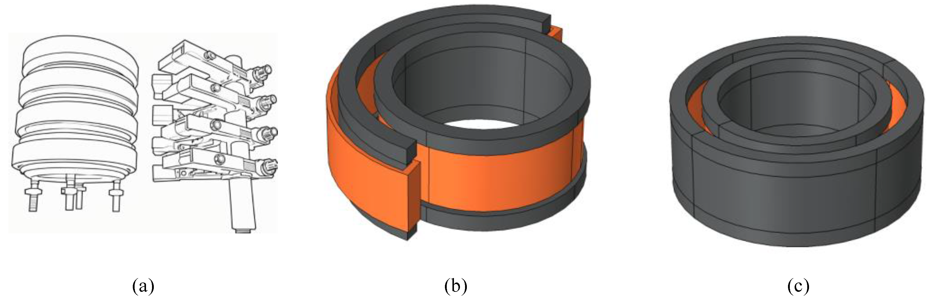
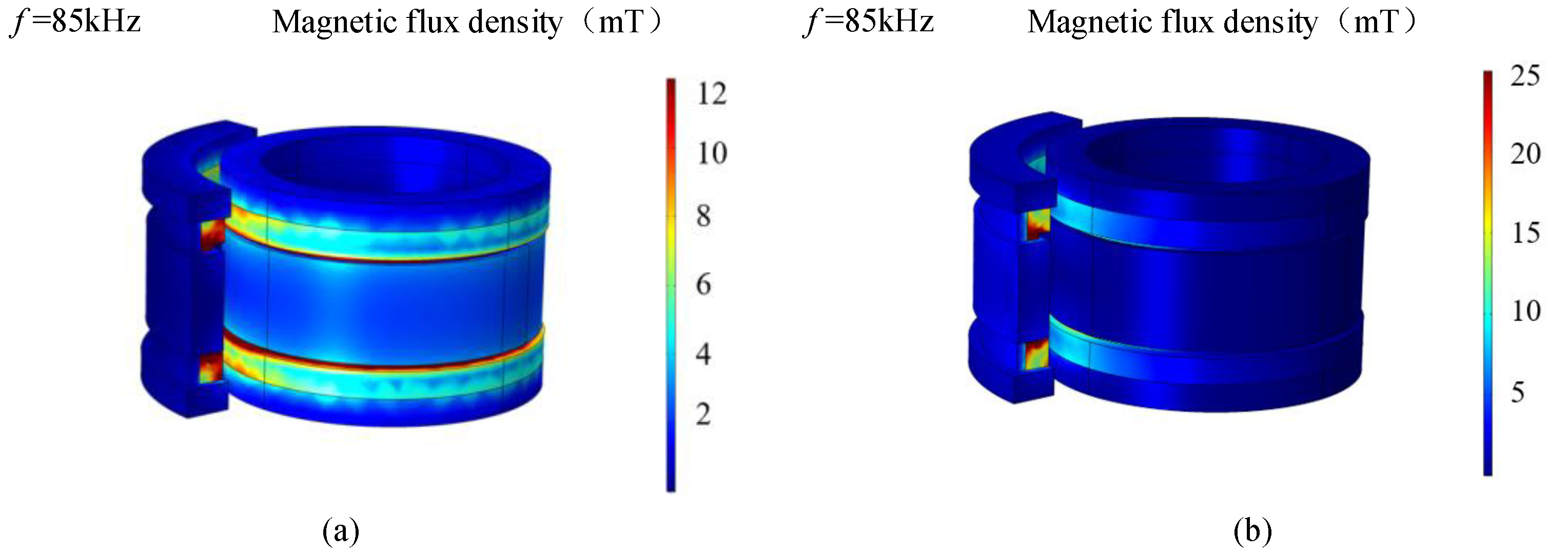
3.2. The Caliper Type Coupler

In some irregular rotating power supply scenarios, such as the traditional conductive slip ring structure shown in Figure 6a, this paper proposes a caliper-type coupler, as shown in Figure 6b, that uses only a part of the nested outer cylinder structure to achieve power transfer. Compared with the traditional nested coupler shown in Figure 6c, the installation of the caliper-type coupler is more convenient, the system’s flexibility is improved, and it is conducive to the replacement and maintenance of the slip ring.
The dimension of the proposed caliper-type coupler is depicted in Figure 7. The inner and outer diameters of the coupler are 100 mm and 160 mm, respectively, the air gap between the inner and outer ring is 10 mm, and the height of the coupler is 60 mm. With the parameters listed in Table 1, the magnetic flux density map of the coupler obtained by applying a 5 A current excitation current to the primary and secondary sides of the coupler using magnetic field simulation software is shown in Figure 8.
When the excitation current increases, the magnetic flux density of the coupler increases. To avoid magnetic saturation, the analysis of the magnetic flux density in the x-axis direction of the system is shown in Figure 9. The maximum magnetic flux density of the system is 12 mT, which is lower than the magnetic saturation threshold of the magnetic core, and the system can work normally.

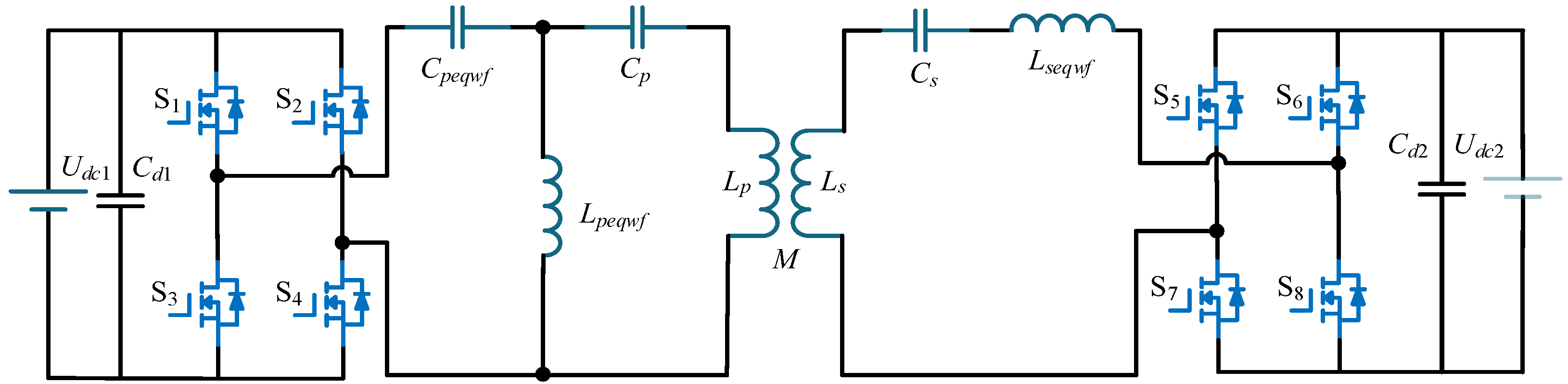
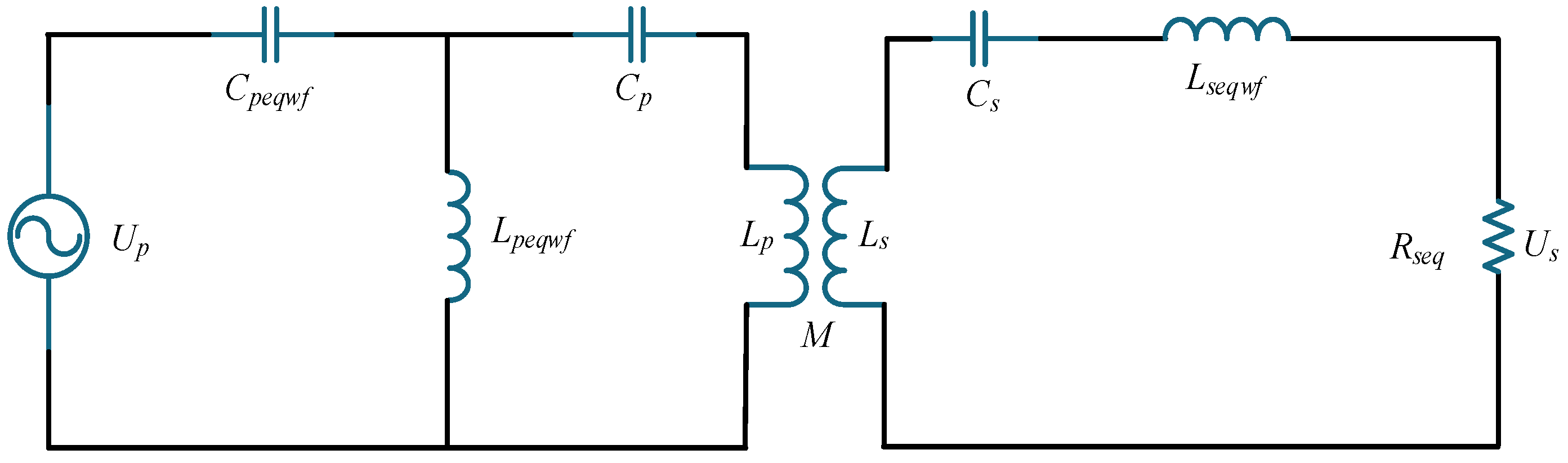
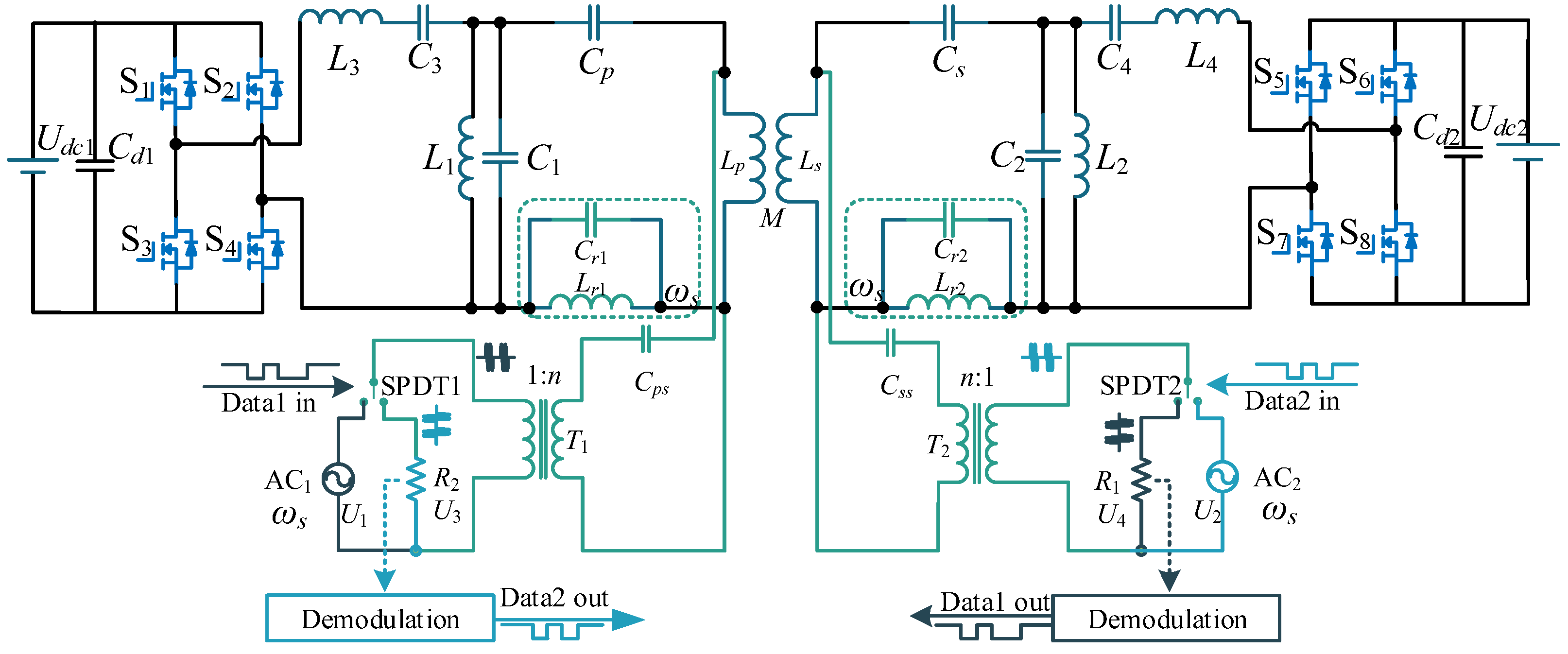
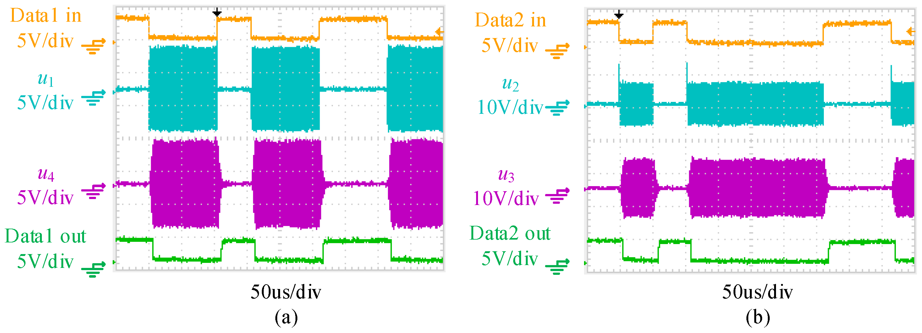
4. Bidirectional Data Transfer Channel

Bidirectional data transfer is achieved through frequency division multiplexing coupling coils, using parallel connection to inject and extract the data carrier and adding an LC parallel network to achieve impedance isolation between the power carrier and data carrier [21]. The injection and extraction method of the BD-SWPDT data carrier is shown in Figure 10.
The lower part of Figure 10 shows the data transfer channel. An LC parallel network is connected in series in the power transfer circuit, and the resonant frequency is set to the data carrier frequency fs, which is much greater than that of the power carrier. When the data carrier is loaded to both ends of the coil, the impedance of the parallel network to the data carrier is relatively large, equivalent to an open circuit, and the equivalent circuit of the data transfer channel is shown in Figure 11. When the power transfer circuit is working, the parallel network is equivalent to the inductor of the network at the power carrier frequency. The impact of the inductance on power transfer can be compensated for by connecting capacitors in series. Due to the pF level capacitance of Cps and Css, the impedances of Cps and Css are very large due to the relatively low-frequency power carrier, and the power carrier can barely flow through the data carrier processing circuit, thus achieving impedance isolation of the power and data transfer channels.
In the data transfer circuit, AC1 and AC2 are the data carrier voltage sources of the primary and secondary sides, respectively. The ASK modulation and loading of the data carrier are achieved by controlling the on–off of the analog switches SPDT1 and SPDT2. Transformers T1 and T2 are used to achieve electrical isolation between the data transfer circuit and the power transfer circuit. R1 is the sampling resistor of the secondary side during forward data transfer, R2 is the sampling resistor of the primary side during reverse data transfer, and the voltages of R1 and R2 are sampled for data demodulation. Cps and Css are series compensation capacitors for the primary and secondary sides of the data transfer channel, and their values satisfy
C p s = 1 ω s 2 L p C s s = 1 ω s 2 L s C r 1 = 1 ω s 2 L r 1 C r 2 = 1 ω s 2 L r 2 ω s = 2 π f s
It should be noted that fs is much greater than ff and fr, the parallel networks (i.e., Lr1, Cr1, and Lr2, Cr2) can be treated as inductors Lr1 and Lr2, respectively, at the relatively low-power transfer frequency, and the values of Lr1, and Lr2 can be directly added to the values of Lp and Ls, respectively, when calculating the other parameters of the system.
Single-pole double throw switches SPDT1 and SPDT2 are connected to sampling resistors by default for receiving signals when there is no data transfer. When data are transmitted in the forward direction, the high- and low-level signals of the data control SPDT1 to modulate the high-frequency carrier. The modulated signal is transmitted to the primary side of transformer T1, and the voltage is stepped up by the transformer T1 and transmitted to the secondary side of transformer T2 through the SS compensation network. After the voltage is stepped down by transformer T2, a sine wave signal is received on resistor R1, and then the data are demodulated through a data demodulation circuit. Due to the symmetrical structure design of the primary and secondary compensation network, the principle of data reverse transfer is consistent with that of forward transfer, thus enabling half duplex communication between the two sides of the wireless power system.

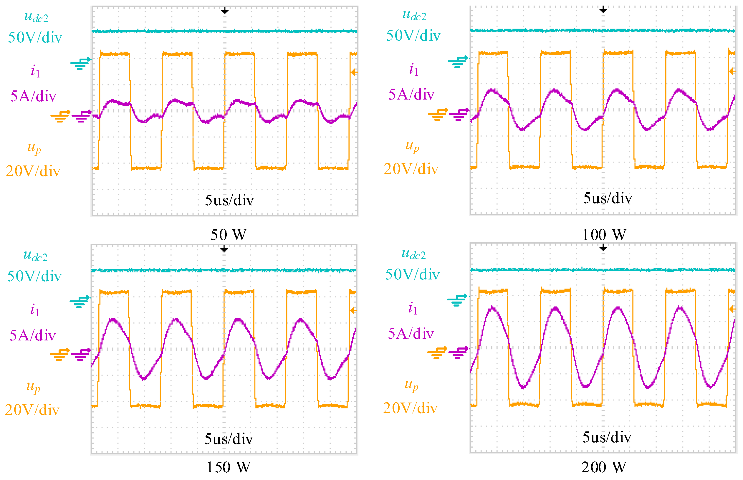
5. Experimental Verification

With the parameters listed in Table 2, an experimental prototype shown in Figure 12, built based on Figure 2 to verify the feasibility of the proposed BD-SWPDT system. The two auxiliary power supplies are used to power the data transceivers. Two USB to TTL converters are utilized to transmit and receive the data through the computer. A DC power supply (ITECH-IT6522C) is used as the DC power source and an electronic load (ITECH-IT8813) is used as the load. In the data transceiver, a direct digital synthesizer (DDS, AD9833) is used to generate the high-frequency data carrier, an analog switch (ADG5419) is used to modulate the data carrier, and an operation amplifier (BUF634) is used as the high-speed buffer to drive the coils.
The procedures for the parameter design of the proposed system are depicted in detail in the flow chart shown in Figure 13. The values of Lpeqwf and Lseqwr can be determined according to the mutual inductance and the transfer gain requirement of the practical application, and other parameters can be calculated from the equations listed.
When power is transferred in the forward and reverse directions, the waveforms of the power transfer channel under different output powers are shown in Figure 14 and Figure 15, respectively. It can be seen from Figure 14 and Figure 15 that the voltage of the inverter is slightly ahead of the inverter current, achieving zero voltage switch, the output voltage almost remains constant under different output powers, and the voltage transfer gain of the forward power transfer is the same with the reverse power transfer. The electronic load is set to constant power mode, and when the output power is 200 W, the efficiencies of the forward and reverse power transfer channel are 88.1% and 88.8%, respectively.
When there is only bidirectional data transfer (without simultaneous power transfer), the waveforms of the data transfer channel are shown in Figure 16. The transmitted data “Data1 in” are modulated and amplified to be converted into modulated signal U1 (blue waveform), which is loaded onto both ends of the transformer. The secondary side receives the signal waveform U4, as shown in the purple waveform, and after demodulation, the data “Data1 out” are restored, as shown in the green waveform. Since the waveforms of “Data1 in” and “Data1 out” are consistent, the data can be transmitted successfully. As can also be seen from Figure 16, no interference occurs on the waveforms of the data transfer channel.
When power and data are transferred simultaneously, the power transfer channel will introduce interference to the data transfer channel, and the waveforms of the data transfer channel are shown in Figure 17. Comparing Figure 16 and Figure 17, it can be inferred that the data transfer channel will be interfered with by the power transfer, but the interference is small, and almost does not affect the normal transfer of data.
The waveforms of the voltage of the coupled coils are also measured when power and data are transferred simultaneously, and are shown in Figure 18. It can be seen from the green circles that high-frequency waves are superimposed on the relatively low-frequency power carrier when the data carrier is transferred, which indicates that power and data are transferred simultaneously via the same coupled coils.
To verify the effect of the proposed power transfer topology on the suppression of power interference, and due to the open circuit characteristics of the parallel networks (L2, C2) and (L1, C1) when power are transferred in the forward direction and the reverse direction, respectively, the waveforms of the data transfer channel are measured and shown in Figure 19. Here, power and data are transferred simultaneously with the LC parallel networks removed. Comparing Figure 19a,b, it can be inferred that the power interference can be significantly suppressed by the proposed topology, resulting in a high-quality transfer of data and reducing the complexity of the data demodulation circuit.

6. Results and Discussion

Table 3 summarizes the performance of this work and relevant works presented in [12,15,16,19,20,21]. It can be inferred from Table 3 that the coupler types of rotary applications can be roughly divided into four categories—the coaxial type, the planar type, the can type, and the caliper type. Due to the coupling structure, the maintenance of the coaxial nested coupler is more inconvenient than other types of couplers. The two sides of the coupler cannot be disassembled separately, which decreases the maintenance flexibility. In practical applications, besides the power transfer, data transfer is of equal importance. However, simultaneous data transfer is not applicable in [12,15,16], which limits its implementation in practical applications. SPWDT technology is proposed in [19,20,21], and this structure and two channels are formed to transfer power and data separately. However, in [20], extra coils are added to transfer data, which will increase the volume and complexity of the coupler. In this work, bidirectional power transfer is also achieved in addition to SWPDT sharing the power transfer coils, and the transfer gains of the two directions can be adjusted independently. When the power transfer channel operates, a large component of harmonics will be generated, which will cause EMI issues. In this work, compensation networks with band-pass filtering characteristics are proposed, suppressing the EMI and creating a favorable condition for data transfer.

7. Conclusions

A non-contact slip ring system with bidirectional simultaneous wireless power and data transfer is proposed in this paper. A caliper-type rotary coupling structure is proposed. Compared with traditional coaxial nested slip rings, it has higher flexibility and easier disassembly and maintenance, and equivalent replacement can be achieved with traditional contact slip rings. The proposed bidirectional constant-voltage LC hybrid compensation topology not only achieves bidirectional constant voltage output, but also filters out most of the high-order harmonics in the power transfer channel, achieving simultaneous high-stability data transfer through the same coupler. The voltage transfer gain of both directions can be adjusted independently according to the application. Finally, the feasibility of the proposed BD-SWPDT system is verified by experiment.

Author Contributions

Methodology, Y.F., Q.C., S.W. and J.X.; validation, Q.C.; writing—original draft, Y.F. and S.W.; writing—review and editing, J.X.; supervision, Z.W. All authors have read and agreed to the published version of the manuscript.

Funding

This research received no external funding.

Data Availability Statement

The original contributions presented in the study are included in the article; further inquiries can be directed to the corresponding authors.

Conflicts of Interest

Author Jing Xiao was employed by the company Guangxi Power Grid Company Ltd., Nanning 530023, China. The remaining authors declare that the research was conducted in the absence of any commercial or financial relationships that could be construed as a potential conflict of interest.

References

  1. Deng, P.; Tang, C.; Sun, M.; Liu, Z.; Hu, H.; Lin, T. EMI Suppression Method for LCC-S MC-WPT Systems by Parameter Optimization. IEEE Trans. Power Electron. 2024, 39, 11134–11147. [Google Scholar] [CrossRef]
  2. Sun, Y.; Liao, Z.-J.; Ye, Z.-H.; Tang, C.-S.; Wang, P.-Y. Determining the Maximum Power Transfer Points for MC-WPT Systems with Arbitrary Number of Coils. IEEE Trans. Power Electron. 2018, 33, 9734–9743. [Google Scholar] [CrossRef]
  3. Zhang, Z.; Georgiadis, A.; Cecati, C. Wireless Power Transfer for Smart Industrial and Home Applications. IEEE Trans. Ind. Electron. 2019, 66, 3959–3962. [Google Scholar] [CrossRef]
  4. Lee, C.-H.; Ho, S.-T.; Hsu, S.-H.; Jiang, J.-A. Taguchi-Based Design of Planar Circular Coils Used in Wireless Charging of Mobile Phones. IEEE Trans. Consum. Electron. 2024, 70, 299–307. [Google Scholar] [CrossRef]
  5. Deng, Z.; Hu, H.; Su, Y.; Chen, F.; Xiao, J.; Tang, C.; Lin, T. Design of a 60-kW EV Dynamic Wireless Power Transfer System with Dual Transmitters and Dual Receivers. IEEE J. Emerg. Sel. Top. Power Electron. 2024, 12, 316–327. [Google Scholar] [CrossRef]
  6. Zhu, J.; Barmada, S.; Musolino, A.; Sani, L. Maintain Power Transmission and Efficiency Tracking Using Variable Capacitors for Dynamic WPT Systems. Electronics 2024, 13, 2853. [Google Scholar] [CrossRef]
  7. Shah, I.A.; Zada, M.; Shah, S.A.A.; Basir, A.; Yoo, H. Flexible Metasurface-Coupled Efficient Wireless Power Transfer System for Implantable Devices. IEEE Trans. Microw. Theory Tech. 2024, 72, 2534–2547. [Google Scholar] [CrossRef]
  8. Fernandez-Munoz, M.; Missous, M.; Sadeghi, M.; Lopez-Espi, P.L.; Sanchez-Montero, R.; Martinez-Rojas, J.A.; Diez-Jimenez, E. Fully Integrated Miniaturized Wireless Power Transfer Rectenna for Medical Applications Tested inside Biological Tissues. Electronics 2024, 13, 3159. [Google Scholar] [CrossRef]
  9. Chen, C.; Jiang, C.; Wang, Y.; Fan, Y.; Luo, B.; Cheng, Y. Compact Curved Coupler With Novel Flexible Nanocrystalline Flake Ribbon Core for Autonomous Underwater Vehicles. IEEE Trans. Power Electron. 2024, 39, 53–57. [Google Scholar] [CrossRef]
  10. Feng, Y.; Sun, Y.; Lin, T.; Hu, H.; Chen, F. Mutual inductance surrogate model of the UWPT system and its constant power optimization at misaligned positions. Wirel. Power Transf. 2024, 11, e001. [Google Scholar] [CrossRef]
  11. Meng, W.; Hu, N.; Lan, H.; Lv, T. Lightweight Design of Magnetic Coupling Mechanism of Wireless Power Transfer System for Underground Rotary Guidance Device. In Proceedings of the 2024 10th International Conference on Power Electronics Systems and Applications (PESA), Hong Kong, China, 5–7 June 2024; pp. 1–4. [Google Scholar] [CrossRef]
  12. Song, K.; Ma, B.; Yang, G.; Jiang, J.; Wei, R.; Zhang, H.; Zhu, C. A Rotation-Lightweight Wireless Power Transfer System for Solar Wing Driving. IEEE Trans. Power Electron. 2019, 34, 8816–8830. [Google Scholar] [CrossRef]
  13. Zhou, Y.; Luo, Y.; Liu, S.; Li, D. An Efficient and Stable Embedded Multi-U-Shaped Column Rotary Transformer. IEEE Trans. Power Electron. 2023, 38, 6734–6743. [Google Scholar] [CrossRef]
  14. Wang, L.; Li, J.; Luo, G.; Si, Q.; Guo, Z.; Peng, Y.; Robertson, I. A Mixed Flux Coupler and Dual-Path Parallel Compensation Based Rotating Wireless Power Transfer System Integrated with Rotational Speed Monitoring Function. IEEE Trans. Power Electron. 2024, 39, 7736–7751. [Google Scholar] [CrossRef]
  15. He, X.; Shu, W.; Yu, B.; Ma, X. Wireless Power Transfer System for Rotary Parts Telemetry of Gas Turbine Engine. Electronics 2018, 7, 58. [Google Scholar] [CrossRef]
  16. Trevisan, R.; Costanzo, A. A 1-kW contactless energy transfer system based on a rotary transformer for sealing rollers. IEEE Trans. Ind. Electron. 2014, 61, 6337–6345. [Google Scholar] [CrossRef]
  17. Zhang, Y.; Yang, J.; Jiang, D.; Li, D.; Qu, R. Design, Manufacture, and Test of a Rotary Transformer for Contactless Power Transfer System. IEEE Trans. Magn. 2022, 58, 8400206. [Google Scholar] [CrossRef]
  18. Li, T.; Wang, Y.; Lang, Z.; Qi, C.; Jin, X.; Chen, X.; Xu, D. Analysis and Design of Rotary Wireless Power Transfer System with Dual-Coupled XLC/S Compensation Topology. IEEE Trans. Ind. Appl. 2023, 59, 2639–2649. [Google Scholar] [CrossRef]
  19. Fan, Y.; Hu, H.; Sun, Y.; Hu, H.; Wu, S. A Simultaneous Wireless Power and Coil Inductance Insensitive Data Transfer System for Rotary Structures. IEEE Trans. Power Electron. 2024, 39, 6526–6536. [Google Scholar] [CrossRef]
  20. Li, X.; Li, Z.; Madawala, U.K.; Wang, H.; Sun, Y.; Dai, X.; Hu, J. A Simultaneous Wireless Power and Data Transfer Method Utilizing a Novel Coupler Design for Rotary Steerable Systems. IEEE Trans. Power Electron. 2024, 39, 11824–11833. [Google Scholar] [CrossRef]
  21. Sun, Y.; Yan, P.-X.; Wang, Z.-H.; Luan, Y.-Y. The Parallel Transmission of Power and Data with the Shared Channel for an Inductive Power Transfer System. IEEE Trans. Power Electron. 2016, 31, 5495–5502. [Google Scholar] [CrossRef]
Figure 1. The BD-SWPDT system’s structural diagram.
Electronics 13 03974 g001
Figure 2. The topology of the BD-WPT system.
Electronics 13 03974 g002
Figure 3. The equivalent circuit of the forward power transfer.
Electronics 13 03974 g003
Figure 4. The further equivalent circuit of the forward power transfer.
Electronics 13 03974 g004
Figure 5. The equivalent circuit of the reverse power transfer.
Electronics 13 03974 g005
Figure 6. (a) The traditional conductive slip ring, (b) the proposed caliper type coupler and (c) the traditional nested coupler.
Electronics 13 03974 g006
Figure 7. The dimensions of the proposed caliper-type coupler.
Electronics 13 03974 g007
Figure 8. The magnetic flux density diagram of the coupler when the excitation current is applied to (a) the inner ring and (b) the outer ring.
Electronics 13 03974 g008
Figure 9. The magnetic flux density with the x coordinate.
Electronics 13 03974 g009
Figure 10. The data carrier injection and extraction.
Electronics 13 03974 g010
Figure 11. The equivalent circuit of the data transfer channel.
Electronics 13 03974 g011
Figure 12. The experimental prototype.
Electronics 13 03974 g012
Figure 13. The flow chart used for parameter design.
Electronics 13 03974 g013
Figure 14. The waveforms of the forward power transfer channel under different output powers.
Electronics 13 03974 g014
Figure 15. The waveforms of the reverse power transfer channel under different output powers.
Electronics 13 03974 g015
Figure 16. The waveforms of the data transfer channel, (a) forward data transfer and (b) reverse data transfer.
Electronics 13 03974 g016
Figure 17. (a) The waveforms of the data transfer channel and (b) its stretched-out view with simultaneous power transferred.
Electronics 13 03974 g017
Figure 18. The waveforms of the data transfer channel and the voltage of the coupled coils.
Electronics 13 03974 g018
Figure 19. The waveforms of the data transfer channel (a) with the LC parallel network and (b) without the LC parallel network.
Electronics 13 03974 g019
Table 1. The parameters of the coupler.
SymbolsUnitValue
Air gap dmm10
Inner ring turns nsTurns15
Outer ring turnsTurns15
Outer ring curvatureDegree90
Table 2. The parameters of the BD-SWPDT system.
SymbolsUnitValuesSymbolsUnitValues
UdcV48fskHz1500
ffkHz85frkHz105
LpμH59LsμH109
MμH27.75n--5
L1μH9.5L2μH14.5
C1nF241C2nF241
L3μH30L4μH35
C3nF61C4nF285
CpnF34.5CsnF23.7
Lr1μH15Lr2μH15
Cr1pF750Cr2pF750
CpspF219CsspF118
Table 3. The performance comparison among the technologies with rotary applications.
References[12][15][16][19][20][21]This Work
Data TransferN/AN/AN/AYYYY
Coupler TypeCoaxial NestedPlanarCan typeCoaxial NestedCoaxial NestedCoaxial NestedCaliper type
Maintenance FlexibilityMediumHighHighMediumMediumMediumHigh
Power TransferUnidirectionalUnidirectionalUnidirectionalUnidirectionalUnidirectionalUnidirectionalBidirectional
Channels1112 (Shared)2 (Separate)2 (Shared)2 (Shared)
Harmonic FilteringN/AN/AN/AYN/AN/AY
Disclaimer/Publisher’s Note: The statements, opinions and data contained in all publications are solely those of the individual author(s) and contributor(s) and not of MDPI and/or the editor(s). MDPI and/or the editor(s) disclaim responsibility for any injury to people or property resulting from any ideas, methods, instructions or products referred to in the content.

