
Enhanced Readout Reliability in Phase Change Memory with a Dual-Sensing-Margin Offset-Compensated Sense Amplifier

Abstract
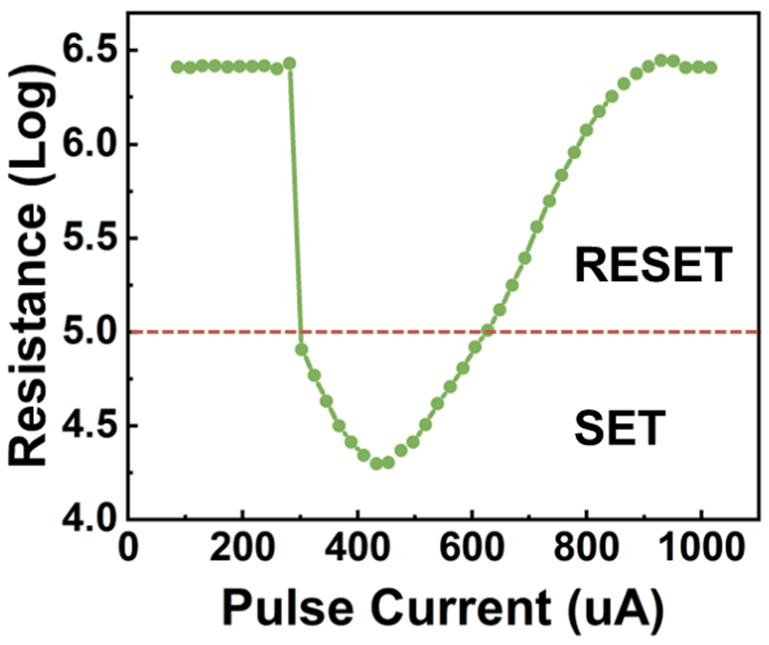
:1. Introduction
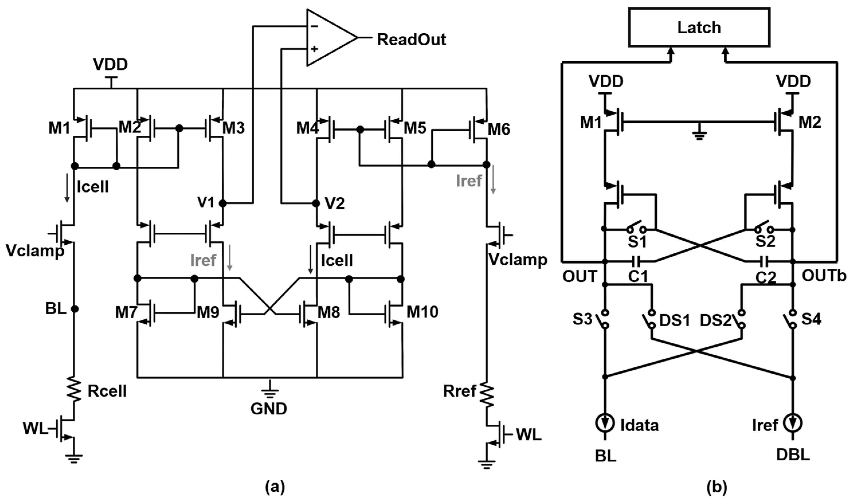
2. Conventional Sense Amplifier Architectures
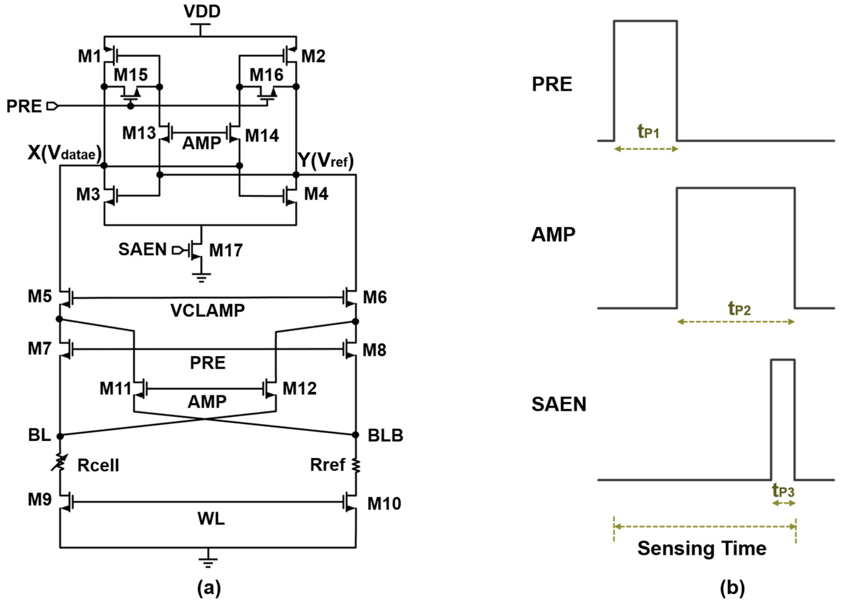
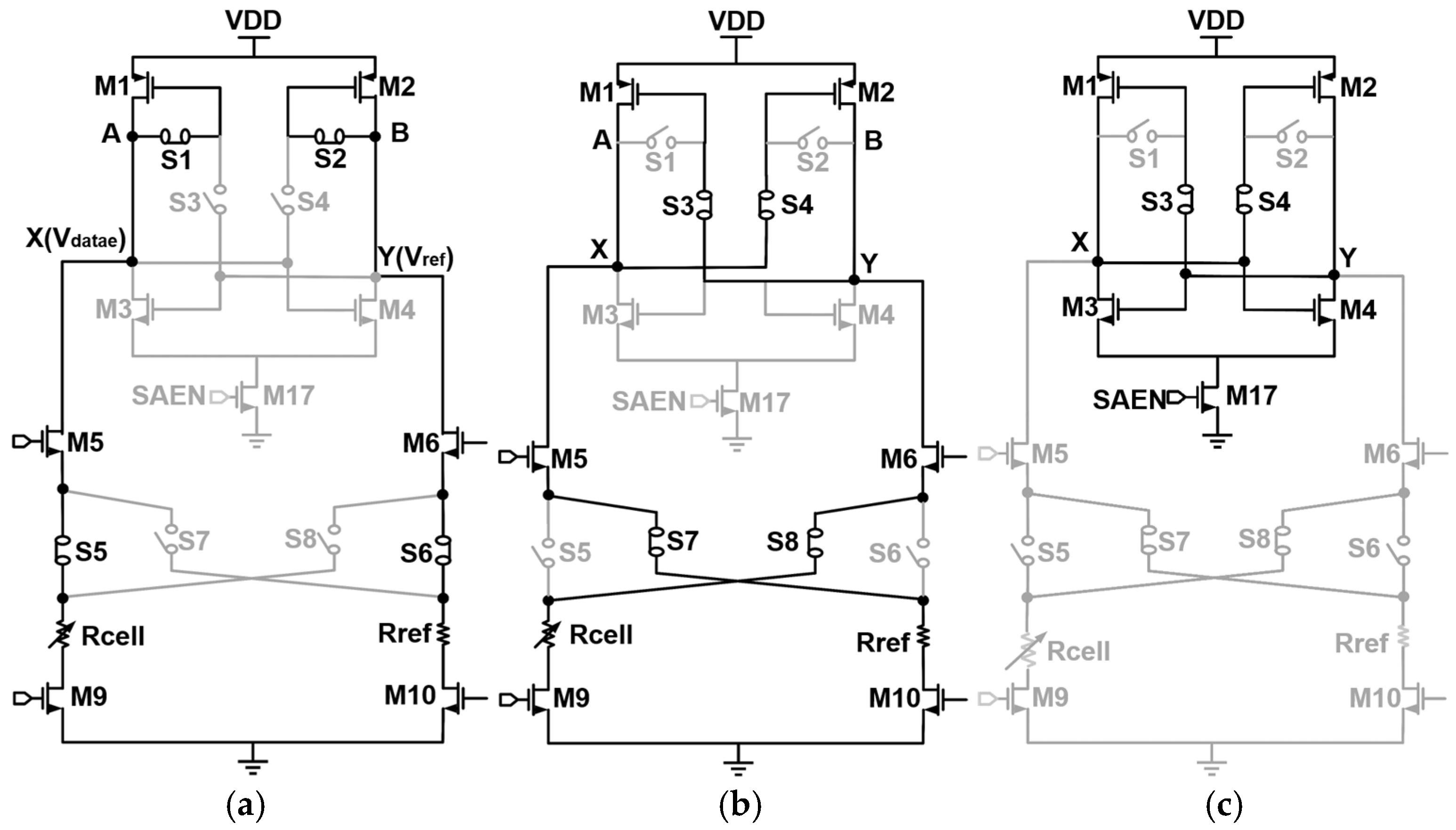
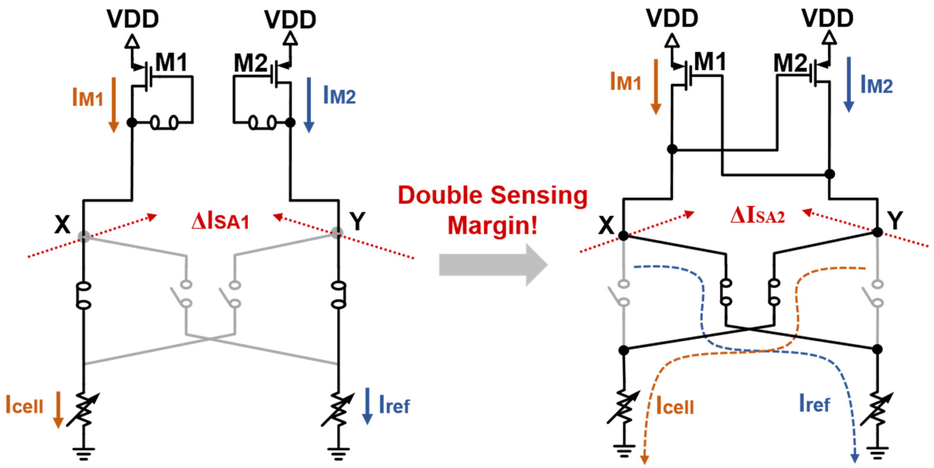
3. Proposed DSOC-SA
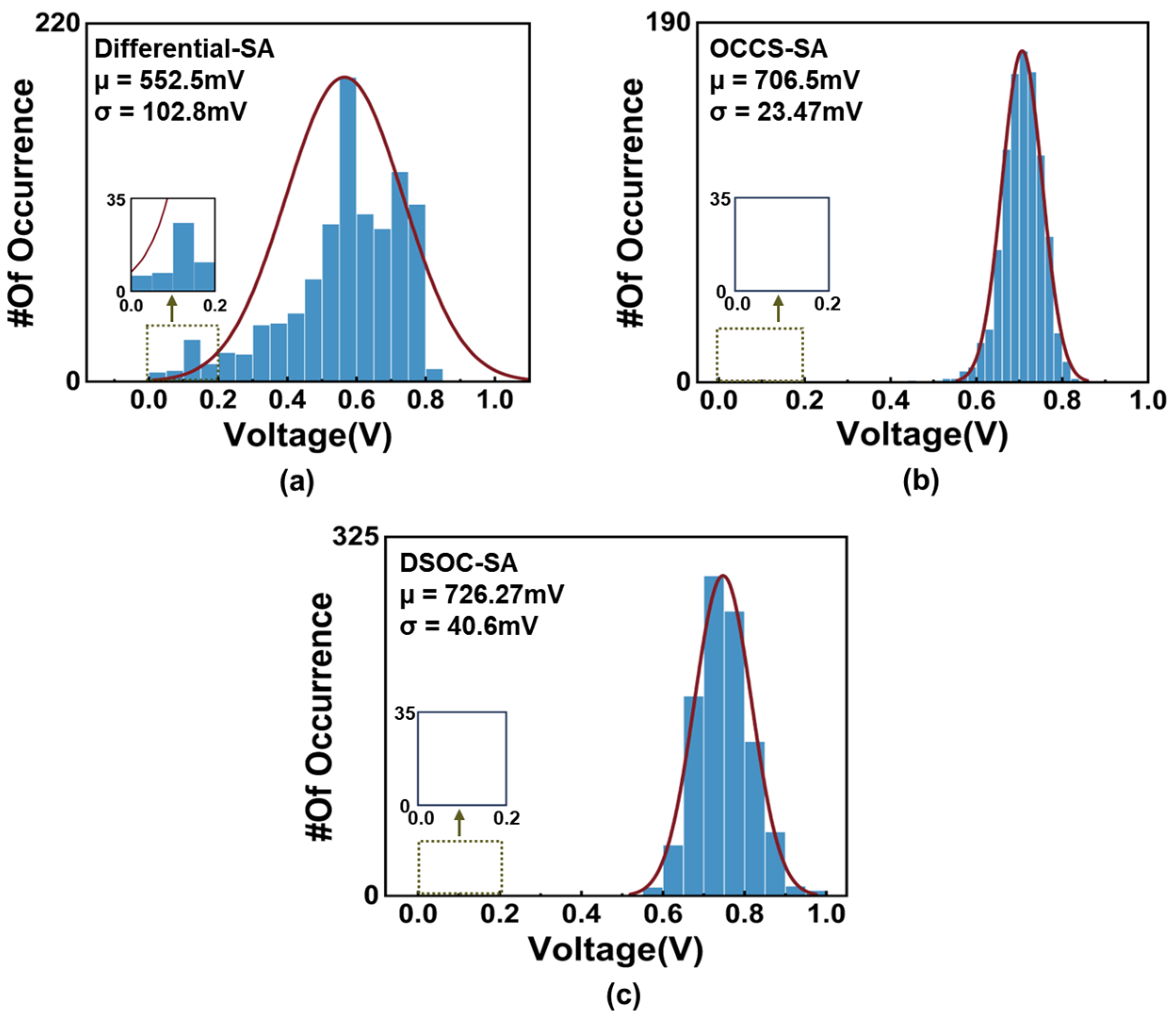
4. Simulations Results and Comparison
5. Conclusions
Author Contributions
Funding
Data Availability Statement
Conflicts of Interest
References
- Daly, D.C.; Fujino, L.C.; Smith, K.C. Through the looking glass—The 2017 edition: Trends in solid-state circuits from ISSCC. IEEE Solid-State Circuits 2017, 9, 12–22. [Google Scholar] [CrossRef]
- Kim, T.; Lee, S. Evolution of phase-change memory for the storage-class memory and beyond. IEEE Trans. Electron Devices 2020, 3, 1394–1406. [Google Scholar] [CrossRef]
- Hosomi, M.; Yamagishi, H.; Yamamoto, T.; Bessho, K.; Higo, Y.; Yamane, K.; Yamada, H.; Shoji, M.; Hachino, H.; Fukumoto, C. A novel nonvolatile memory with spin torque transfer magnetization switching: Spin-RAM. In Proceedings of the IEEE International Electron Devices Meeting, Washington, DC, USA, 5 December 2005; pp. 459–462. [Google Scholar]
- Levisse, A.; Giraud, B.; Noel, J.-P.; Moreau, M.; Portal, J.-M. RRAM crossbar arrays for storage class memory applications: Throughput and density considerations. In Proceedings of the 2018 Conference on Design of Circuits and Integrated Systems (DCIS), Lyon, France, 14–16 November 2018; pp. 1–6. [Google Scholar]
- Meo, A.; Chureemart, P.; Wang, S.; Chepulskyy, R.; Apalkov, D.; Chantrell, R.; Evans, R.F.L. Thermally nucleated magnetic reversal in CoFeB/MgO nanodots. Sci. Rep. 2017, 7, 16729. [Google Scholar] [CrossRef] [PubMed]
- Ishibe, T.; Maeda, Y.; Terada, T.; Naruse, N.; Mera, Y.; Kobayashi, E.; Nakamura, Y. Resistive switching memory performance in oxide hetero-nanocrystals with well-controlled interfaces. Sci. Technol. Adv. Mater. 2020, 21, 195–204. [Google Scholar] [CrossRef] [PubMed]
- Lee, S.; Jeong, J.H.; Lee, T.S.; Kim, W.M.; Cheong, B.K. Bias polarity dependence of a phase change memory with a Ge-doped SbTe: A method for multilevel programing. Appl. Phys. Lett. 2008, 92, 243507. [Google Scholar] [CrossRef]
- Fong, S.W.; Neumann, C.M.; Wong, H.S. Phase-change memory—Towards a storage-class memory. IEEE Trans. Electron Devices 2017, 64, 4374–4385. [Google Scholar] [CrossRef]
- Raoux, S.; Burr, G.W.; Breitwisch, M.J.; Rettner, C.T.; Chen, Y.-C.; Shelby, R.M. Phase-change random access memory: A scalable technology. IBM J. Res. Dev. 2008, 52, 465–479. [Google Scholar] [CrossRef]
- Giannopoulos, I.; Sebastian, A.; Le Gallo, M.; Jonnalagadda, V.P.; Sousa, M.; Boon, M.N. 8-bit Precision In-Memory Multiplication with Projected Phase-Change Memory. In Proceedings of the 2018 IEEE International Electron Devices Meeting (IEDM), San Francisco, CA, USA, 1–5 December 2018; pp. 27.7.1–27.7.4. [Google Scholar]
- Papandreou, N.; Pantazi, A.; Sebastian, A.; Breitwisch, M.; Lam, C.; Pozidis, H. Multilevel phase-change memory. In Proceedings of the 2010 17th IEEE International Conference on Electronics, Circuits and Systems, Athens, Greece, 12–15 December 2010; pp. 1017–1020. [Google Scholar]
- Papandreou, N.; Pozidis, H.; Pantazi, A.; Sebastian, A.; Breitwisch, M.; Lam, C. Programming algorithms for multilevel phase-change memory. In Proceedings of the 2011 IEEE International Symposium of Circuits and Systems (ISCAS), Rio de Janeiro, Brazil, 15–18 May 2011; pp. 329–332. [Google Scholar]
- Nair, P.J.; Chou, C.; Rajendran, B.; Qureshi, M.K. Reducing read latency of phase change memory via early read and Turbo Read. In Proceedings of the 2015 IEEE 21st International Symposium on High Performance Computer Architecture (HPCA), Burlingame, CA, USA, 7–11 February 2015; pp. 309–319. [Google Scholar]
- Liu, J.; Wang, X.; Wang, Q.; Wu, D.; Zhang, Z.; Pan, L.; Liu, M. A low-voltage sense amplifier for high-performance embedded flash memory. J. Semicond. 2011, 31, 105001. [Google Scholar]
- Campardo, G.; Micheloni, R.; Novosel, D. VLSI-Design of Non-Volatile Memories; Springer: Berlin/Heidelberg, Germany, 2005; pp. 269–331. [Google Scholar]
- Li, X.; Chen, H.; Song, Z. Design and analysis of a high-performance sense amplifier for Phase-Change Memory. In Proceedings of the International Conference on Computer Research and Development, Shanghai, China, 11–13 March 2011; Volume 3, pp. 318–321. [Google Scholar]
- Li, X.; Chen, H.; Xie, C.; Cai, D.; Song, S.; Chen, Y.; Lei, Y.; Zhu, M.; Song, Z. Enhancing the performance of phase change memory for embedded applications. Phys. Status Solidi (RRL)–Rapid Res. Lett. 2019, 13, 1800558. [Google Scholar] [CrossRef]
- Lei, Y.; Chen, H.; Wang, Q.; Li, X.; Li, X.; Tian, Z.; Song, Z.; Briefs, S. A single-reference parasitic-matching sensing circuit for 3-D cross point PCM. IEEE Trans. Circuits Syst. II Express Briefs 2017, 65, 486–490. [Google Scholar] [CrossRef]
- Shin, M.; Kong, B. A Pseudo-Differential High-Speed Sensing Scheme for Phase-Change Memory. In Proceedings of the International Conference on Circuits, Systems and Simulation, Nanjing, China, 13–15 May 2023; pp. 97–101. [Google Scholar]
- Na, T.; Song, B.; Kim, J.P.; Kang, S.H.; Jung, S. Offset-canceling current-sampling sense amplifier for resistive nonvolatile memory in 65 nm CMOS. IEEE J. Solid-State Circuits 2016, 52, 496–504. [Google Scholar] [CrossRef]
- Chang, M.; Shen, S.; Liu, C.; Wu, C.; Lin, Y.; King, Y.; Lin, C.; Liao, H.; Chih, Y.; Yamauchi, H. An offset-tolerant fast-random-read current-sampling-based sense amplifier for small-cell-current nonvolatile memory. IEEE J. Solid-State Circuits 2014, 48, 864–877. [Google Scholar] [CrossRef]
- Cho, W.Y.; Cho, B.H.; Choi, B.G.; Oh, H.R.; Kang, S.; Kim, K. A 0.18-/spl mu/m 3.0-V 64-Mb nonvolatile phase-transition random access memory (PRAM). IEEE J. Solid-State Circuits 2005, 40, 293–300. [Google Scholar]
- Atwood, G. Phase-Change Materials for Electronic Memories. Science 2008, 321, 210–211. [Google Scholar] [CrossRef] [PubMed]
- Gallo, M.L.; Athmanathan, A.; Krebs, D.; Sebastian, A. Evidence for thermally assisted threshold switching behavior in nanoscale phase-change memory cells. J. Appl. Phys. 2016, 119, 025704. [Google Scholar] [CrossRef]
- Ko, J.; Kim, J.; Choi, Y.; Park, H.K.; Jung, S.C.; Papers, S.I.R. Temperature-tracking sensing scheme with adaptive precharge and noise compensation scheme in PRAM. IEEE Trans. Circuits Syst. I Regul. Pap. 2016, 62, 2091–2102. [Google Scholar] [CrossRef]
- Jo, K.; Yoon, H.C.; Briefs, S.I.E. Variation-tolerant sensing circuit for ultralow-voltage operation of spin-torque transfer magnetic RAM. IEEE Trans. Circuits Syst. II Express Briefs 2017, 64, 570–574. [Google Scholar] [CrossRef]
- Stern, K.; Keller, Y.; Christopher, M. Neumann; Eric Pop; Eilam Yalon. Temperature-dependent thermal resistance of phase change memory. Appl. Phys. Lett. 2022, 120, 113501. [Google Scholar] [CrossRef]
- Kashem, M.B.; Scoggin, J.; Woods, Z.; Silva, H.; Gokirmak, A. Modeling Reset, Set and Read Operations in Nanoscale Ge2Sb2Te5 Phase Change Memory Devices Using Electric Field and Temperature Dependent Material Properties. Phys. Status Solidi (RRL)—Rapid Res. Lett. 2023, 17, 2200419. [Google Scholar] [CrossRef]


| Parameter | Value |
|---|---|
| VDD | 1.1 V |
| RREF | 100 K |
| RSET (µ) | 50 K |
| RSET (σ) | 10 K |
| RRESET (µ) | 200 K |
| RRESET (σ) | 45 K |
| Temperature (°C) | State | µΔV (mV) | σΔV (mV) | RAPYCELL (σ) |
|---|---|---|---|---|
| −40 | 0 | 733.14 | 119.7 | 6.04 |
| 1 | 606.9 | 60.7 | 9.5 | |
| 27 | 0 | 739.3 | 66.7 | 10.62 |
| 1 | 703.1 | 83.3 | 8.21 | |
| 85 | 0 | 707.9 | 69.3 | 9.81 |
| 1 | 682.4 | 42.6 | 14.5 |
| Differential SA [10] | OCCS-SA [13] | This Work (DSOC-SA) | |
|---|---|---|---|
| VDD | 1.1 V | 1.1 V | 1.1 V |
| Offset Cancelation | X | √ | √ |
| Area Consumption | Large | Large | Small |
| Sensing Time | 19.6 ns | 5.5 ns | 3.5 ns |
| Average Read Energy/Bit | 792 fJ | 209 fJ | 102 fJ |
Disclaimer/Publisher’s Note: The statements, opinions and data contained in all publications are solely those of the individual author(s) and contributor(s) and not of MDPI and/or the editor(s). MDPI and/or the editor(s) disclaim responsibility for any injury to people or property resulting from any ideas, methods, instructions or products referred to in the content. |
© 2024 by the authors. Licensee MDPI, Basel, Switzerland. This article is an open access article distributed under the terms and conditions of the Creative Commons Attribution (CC BY) license (https://creativecommons.org/licenses/by/4.0/).
Share and Cite
Wu, Q.; Xie, C.; Song, S.; Ding, X.; Li, X.; Song, Z. Enhanced Readout Reliability in Phase Change Memory with a Dual-Sensing-Margin Offset-Compensated Sense Amplifier. Electronics 2024, 13, 4488. https://doi.org/10.3390/electronics13224488
Wu Q, Xie C, Song S, Ding X, Li X, Song Z. Enhanced Readout Reliability in Phase Change Memory with a Dual-Sensing-Margin Offset-Compensated Sense Amplifier. Electronics. 2024; 13(22):4488. https://doi.org/10.3390/electronics13224488
Chicago/Turabian StyleWu, Qingyu, Chenchen Xie, Sannian Song, Xing Ding, Xi Li, and Zhitang Song. 2024. "Enhanced Readout Reliability in Phase Change Memory with a Dual-Sensing-Margin Offset-Compensated Sense Amplifier" Electronics 13, no. 22: 4488. https://doi.org/10.3390/electronics13224488
APA StyleWu, Q., Xie, C., Song, S., Ding, X., Li, X., & Song, Z. (2024). Enhanced Readout Reliability in Phase Change Memory with a Dual-Sensing-Margin Offset-Compensated Sense Amplifier. Electronics, 13(22), 4488. https://doi.org/10.3390/electronics13224488