
A Tight Load Regulation Hysteretic Boost Converter with Compact and Energy-Efficient Anti-Phase Emulated Current Control †

Abstract
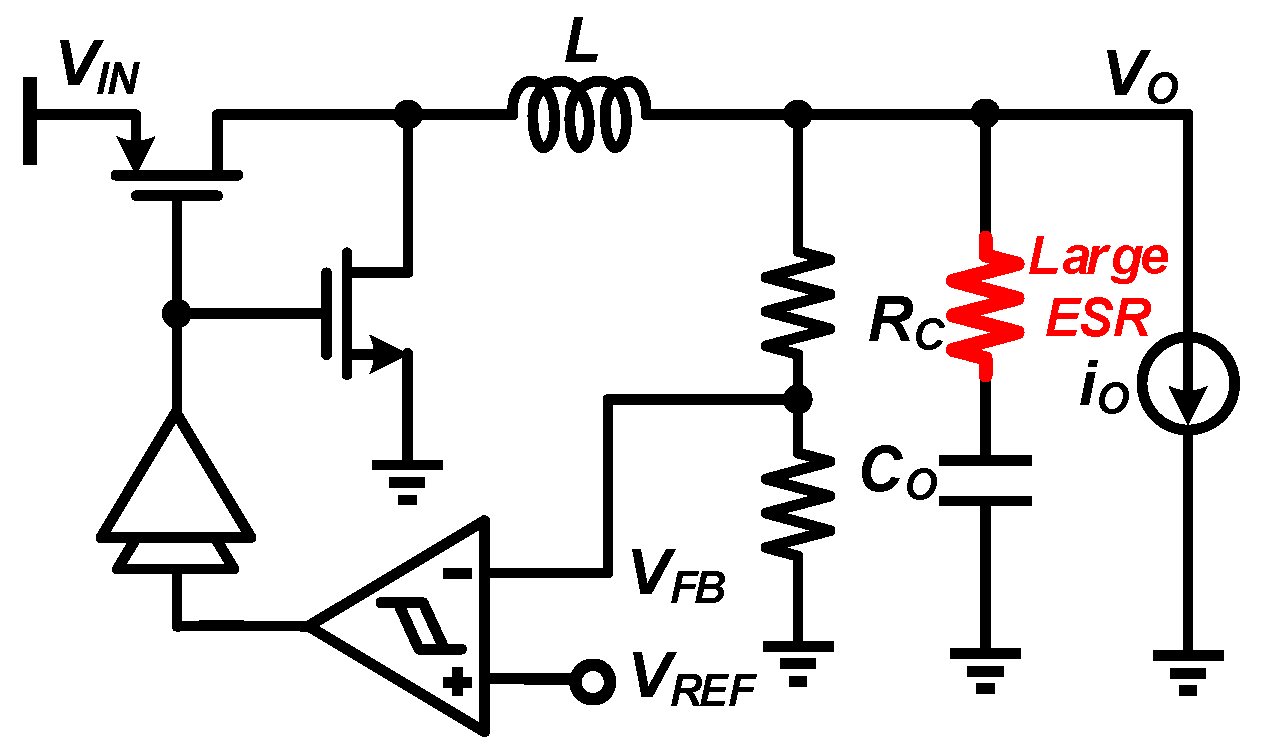
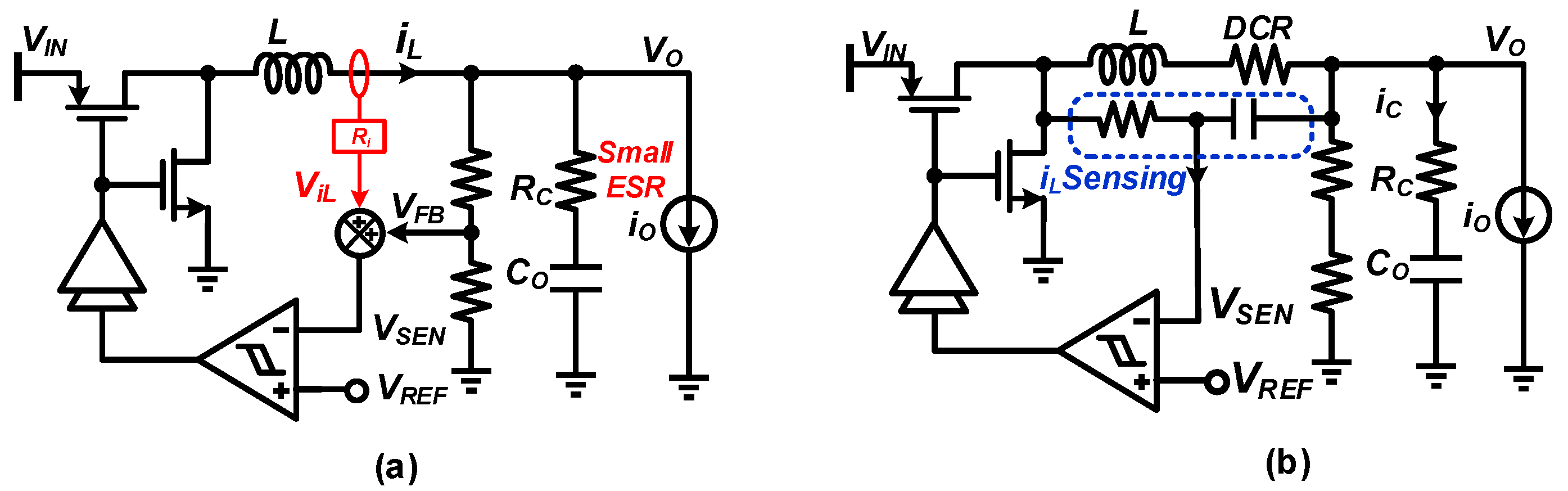
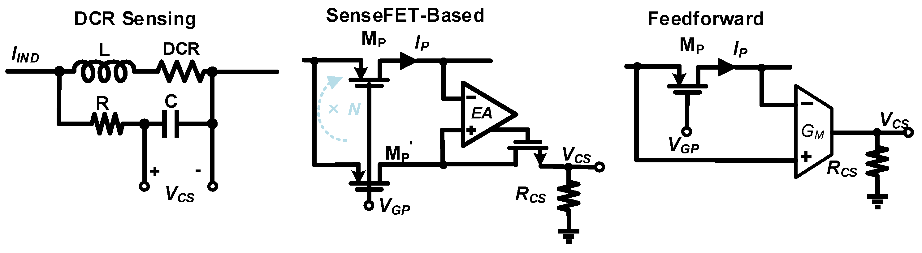
:1. Introduction
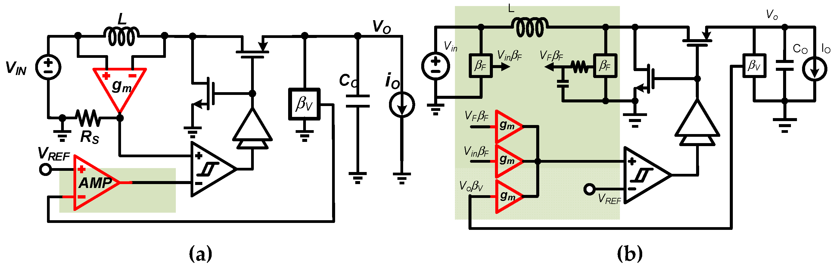
2. Architecture and Circuit Implementation
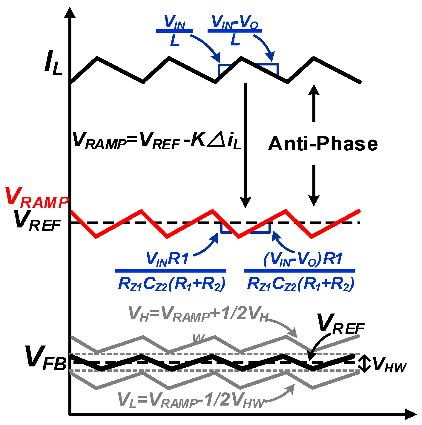
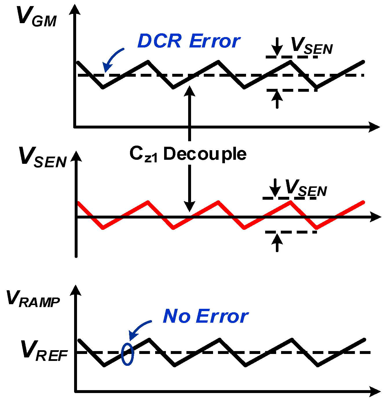
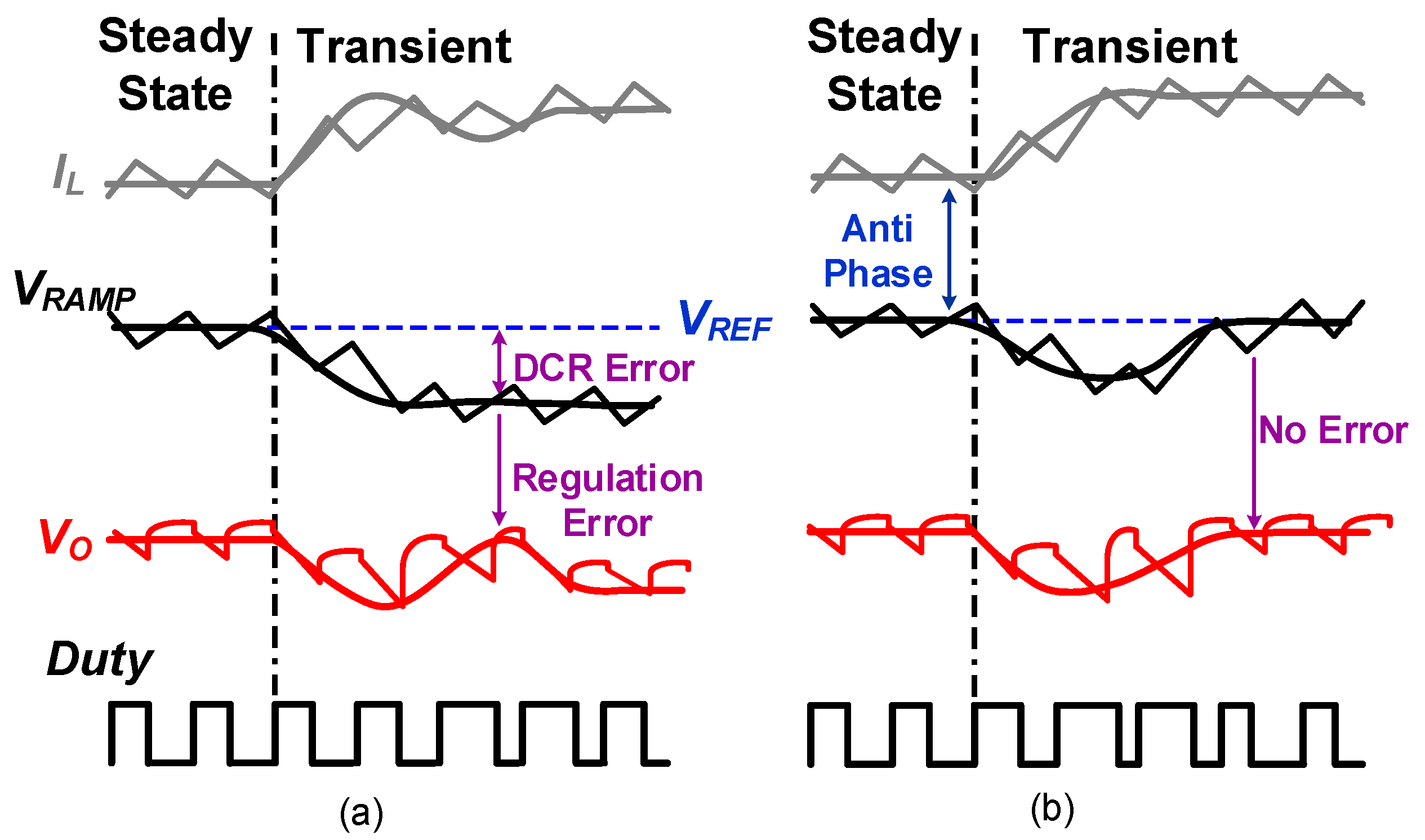
2.1. System Architecture
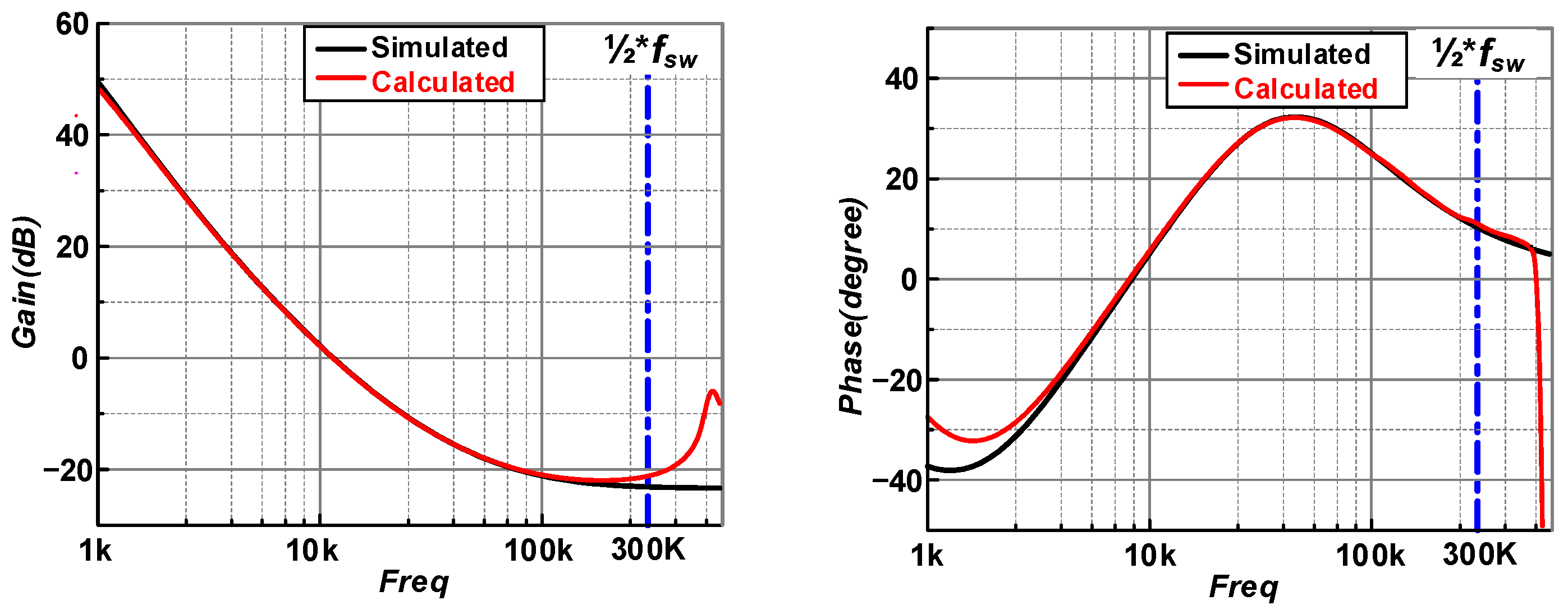
2.2. Stability Analyses
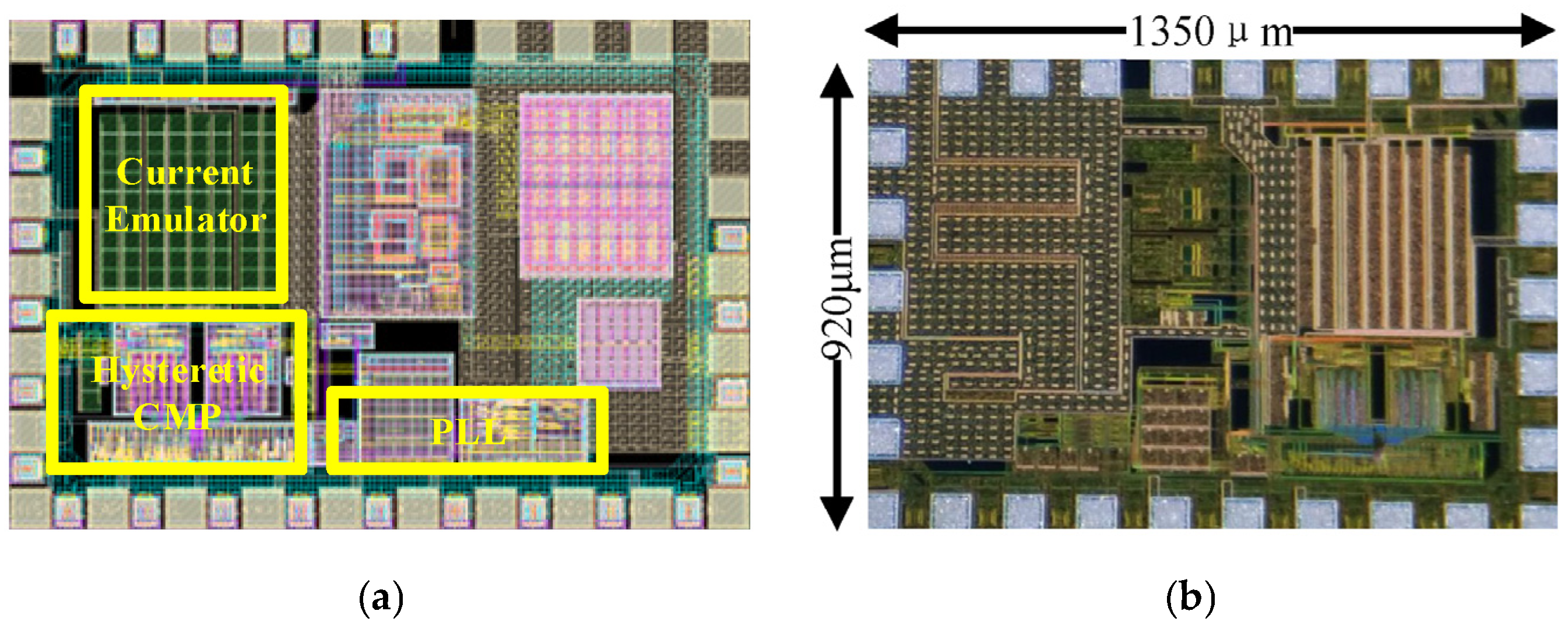
2.3. Circuit Implementation
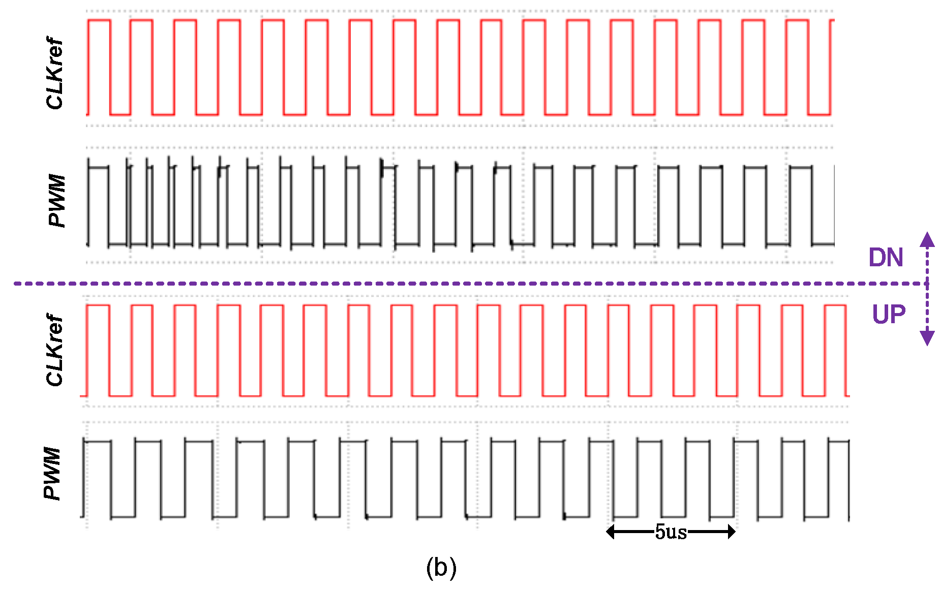
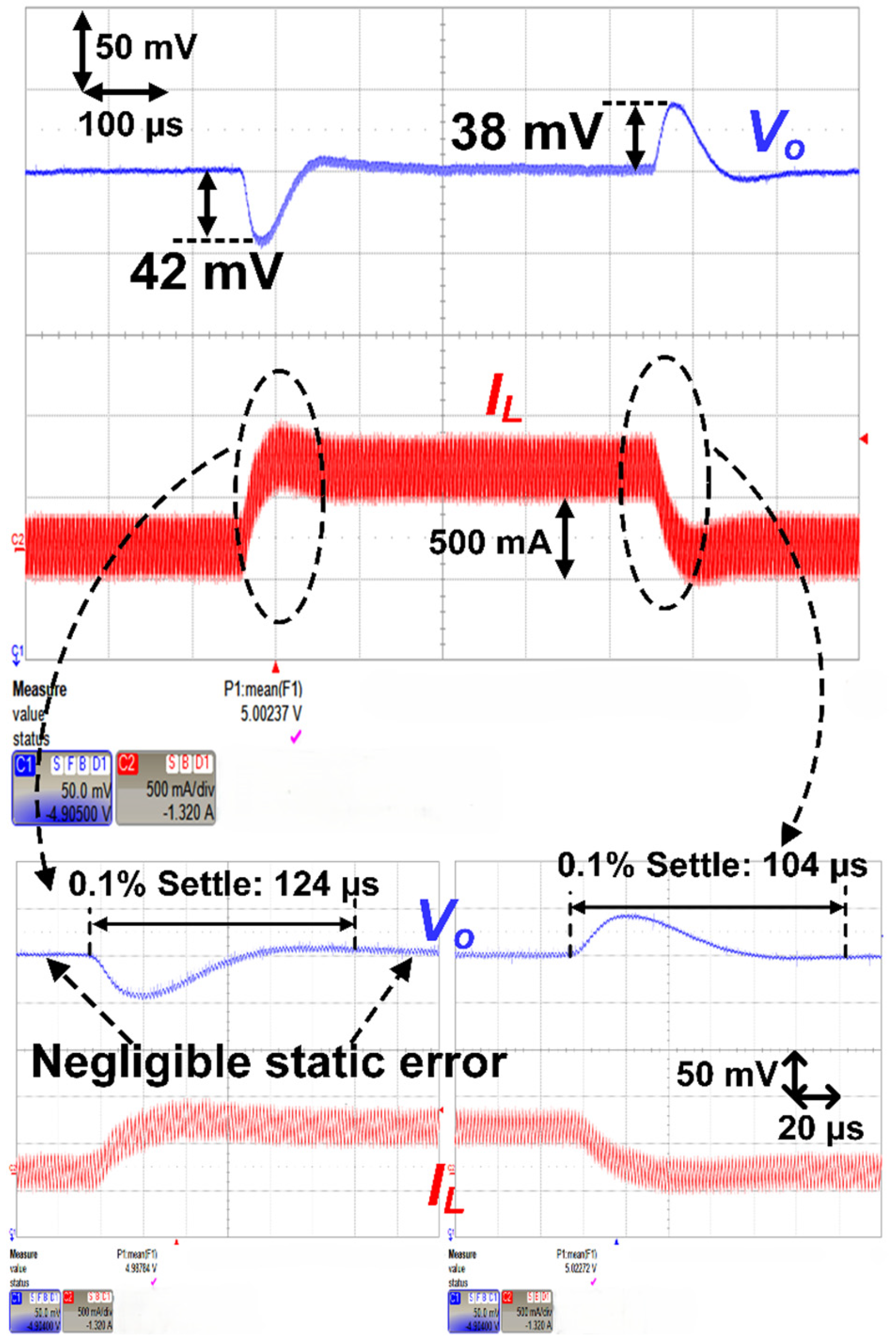
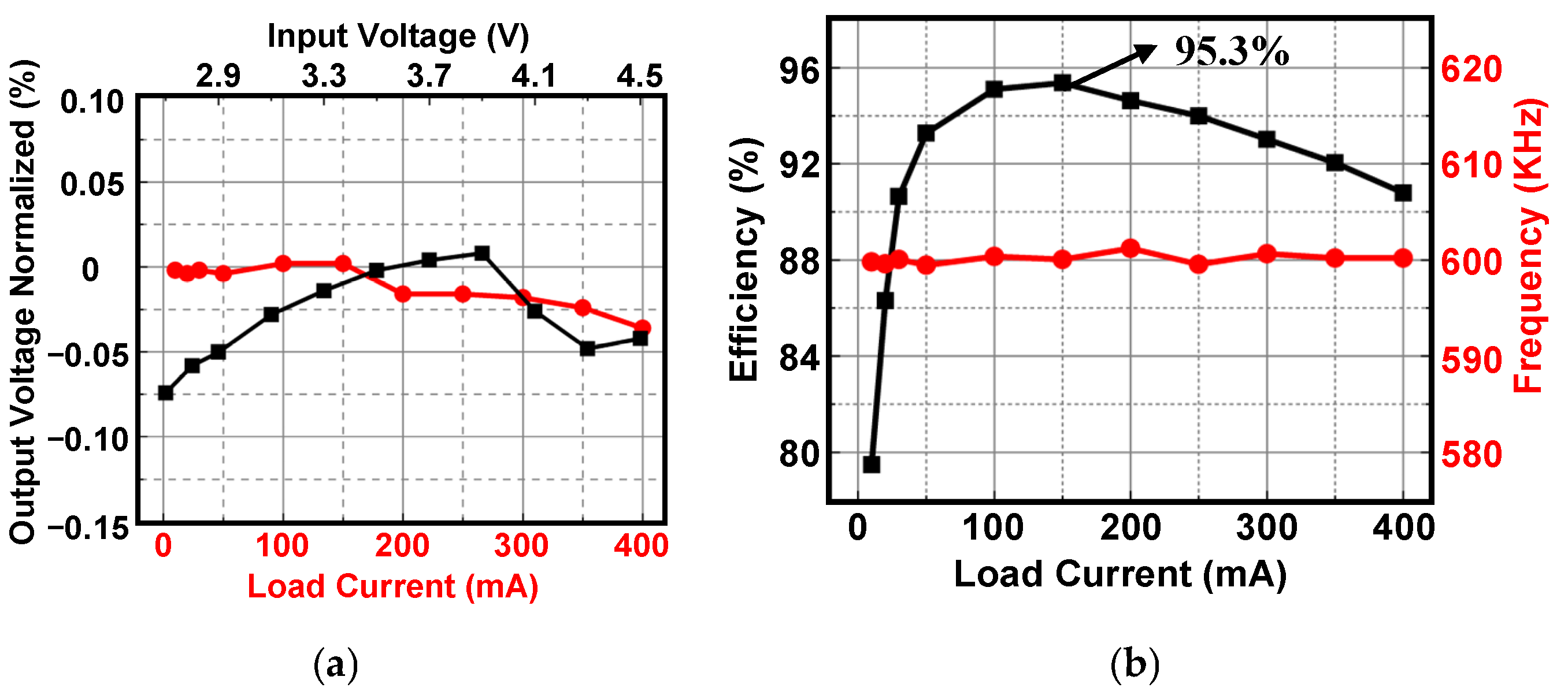
3. Measure Results
4. Discussion
Author Contributions
Funding
Data Availability Statement
Conflicts of Interest
Correction Statement
Appendix A

| Abbreviations | Meaning |
|---|---|
| DCR | Inductor series resistance |
| PLL | Phase-locked loop |
| CM | current-mode |
| PWM | Pulse width modulation |
| OTA | Operational transconductance amplifier |
| GM | Transconductance |
| PFD | Phase-frequency detector |
| Symbol | Meaning |
|---|---|
| VIN | The input voltage of the system |
| VO | The output voltage of the system |
| IL(iL) | The inductor current |
| IO(iO) | The output current |
| VREF | Reference voltage |
| VFB | Output feedback voltage |
| CLKREF | System clock |
| VRAMP | The output voltage of the proposed anti-phase current emulator, which includes the information of the inductor current |
| VHW | Hysteretic band window |
| fsw | Switching frequency |
References
- Venkatesh, G.K. An enhanced digital control loop of Boost converter in Low Power Microcontrollers. In Proceedings of the 2024 IEEE 13th International Conference on Communication Systems and Network Technologies (CSNT), Jabalpur, India, 6–7 April 2024; pp. 1261–1264. [Google Scholar]
- Singh, A.; Gupta, J.; Singh, B. Bridgeless Modified High-Step-Up Gain SEPIC PFC Converter Based Charger for Light EVs Battery. IEEE Trans. Ind. Appl. 2023, 59, 6155–6166. [Google Scholar] [CrossRef]
- Hasanpour, S.; Lee, S.S. A New Quadratic DC/DC Converter with Ultrahigh Voltage Gain. IEEE Trans. Power Electron. 2024, 39, 8800–8812. [Google Scholar] [CrossRef]
- Melillo, P.; Zaffin, S.; Leoncini, M.; Brunero, A.; Gasparini, A.; Levantino, S.; Ghioni, M. A Wide-Input-Range Time-Based Buck Converter with Adaptive Gain and Continuous Phase Preset for Seamless PFM/PWM Transitions. IEEE Trans. Circuits Syst. I Regul. Pap. 2024, 71, 3436–3447. [Google Scholar] [CrossRef]
- Kim, S.J.; Choi, W.S.; Pilawa-Podgurski, R.; Hanumolu, P.K. A10-MHz 2–800-mA 0.5–1.5-V 90% Peak Efficiency Time-Based Buck Converter with Seamless Transition Between PWM/PFM Modes. IEEE J. Solid-State Circuits 2018, 53, 814–824. [Google Scholar] [CrossRef]
- Alevoor, S.; Nayak, R.D.; Talele, B.; Ray, A.; Rutkowski, J.D.; Stockstad, T.; Bakkaloglu, B. A 95.2% Efficiency DC–DC Boost Converter Using Peak Current Fast Feedback Control (PFFC) for Improved Load Transient Response. IEEE Trans. Circuits Syst. I 2023, 70, 1097–1109. [Google Scholar] [CrossRef]
- Santoro, F.; Kuhn, R.; Gibson, N.; Rasera, N.; Tost, T.; Graeb, H.; Brederlow, R. A Hysteretic Buck Converter with 92.1% Maximum Efficiency Designed for Ultra-Low Power and Fast Wake-Up SoC Applications. IEEE J. Solid-State Circuits. 2018, 53, 1856–1868. [Google Scholar] [CrossRef]
- Jung, D.H.; Kim, K.; Joo, S.; Jung, S.O. 0.293-mm2 Fast Transient Response Hysteretic Quasi-V2 DC-DC Converter with Area-Efficient Time-Domain-Based Controller in 0.35um CMOS. IEEE J. Solid-State Circuits. 2018, 53, 1844–1855. [Google Scholar] [CrossRef]
- Li, Y.-C.; Chen, C.-J.; Tsai, C.-J. A Constant On-Time Buck Converter with Analog Time-Optimized On-Time Control. IEEE Trans. Power Electron. 2020, 35, 3754–3765. [Google Scholar] [CrossRef]
- Ting, C.Y.; Lin, J.Y.; Chen, C.C.P. AQuasi-V2 Hysteretic Buck Converter with Adaptive COT Control for Fast DVS and Load-Transient Response in RF Applications. IEEE Trans. Circuits Syst. II 2020, 67, 531–535. [Google Scholar]
- Kumar, V.I.; Kapat, S. Digital Hysteretic Average Current Control for Fast Recovery in a Non-Inverting Buck-Boost Converter. In Proceedings of the 2021 IEEE Applied Power Electronics Conference and Exposition (APEC), Phoenix, AZ, USA, 14–17 June 2021; pp. 474–481. [Google Scholar]
- Lee, K.; Kim, H.; Yoon, J.; Oh, H.-S.; Park, J.-H.; Park, B.-H.; Park, H.; Lee, Y. An Asynchronous Boost Converter with Time-Based Dual-Mode Control for Wide Load Range and High Efficiency in SSD Applications. IEEE Trans. Ind. Electron. 2020, 67, 10520–10530. [Google Scholar] [CrossRef]
- Qu, W.; Gu, D.; Cao, H.; Yang, X.; Xi, J.; He, L.; Dong, S. A 95.3% Peak Efficiency 38mV overshoot and 5mV/A load regulation Hysteretic Boost Converter with Anti-Phase Emulate Current Control. In Proceedings of the ESSCIRC 2019—IEEE 45th European Solid State Circuits Conference (ESSCIRC), Cracow, Poland, 23–26 September 2019; pp. 133–136. [Google Scholar]
- Hong, W.; Lee, M. A15–25-MHz and 1-µs/0.4-A Load Response AOT Boost Converter Using an Accurate Feedforward-Path Current Sensor. IEEE Trans. Power Electron. 2022, 37, 1205–1209. [Google Scholar]
- Yang, W.-H.; Huang, C.-J.; Huang, H.-H.; Lin, W.-T.; Chen, K.-H.; Lin, Y.-H.; Lin, S.-R.; Tsai, T.-Y. A constant-on-time control DC-DC buck converter with the pseudowave tracking technique for regulation accuracy and load transient enhancement. IEEE Trans. Power Electron. 2018, 33, 6187–6198. [Google Scholar] [CrossRef]
- Amir, S.; van der Zee, R.; Nauta, B. A self-oscillating boosting am-plifier with adaptive soft switching control for piezoelectric transducers. IEEE J. Solid-State Circuits 2019, 54, 253–265. [Google Scholar] [CrossRef]
- Ain, Q.U.; Khan, D.; Jang, B.G.; Basim, M.; Shehzad, K.; Asif, M.; Verma, D.; Ali, I.; Pu, Y.G.; Hwang, K.C.; et al. A High-Efficiency Fast Transient COT Control DC–DC Buck Converter with Current Reused Current Sensor. IEEE Trans. Power Electron. 2021, 36, 4479–4484. [Google Scholar]
- Hong, W.; Lee, M. A 10-MHz current-mode AOT boost converter with dual-ramp modulation scheme and translinear loop-based current sensor for wifi IoT applications. IEEE J. Solid-State Circuits 2021, 56, 2388–2401. [Google Scholar] [CrossRef]
- Tsai, J.-C.; Chen, C.-L.; Lee, Y.-H.; Yang, H.-Y.; Hsu, M.-S.; Chen, K.-H. Modified Hysteretic Current Control (MHCC) for Improving Transient Response of Boost Converter. IEEE TCASI 2011, 58, 1967–1979. [Google Scholar] [CrossRef]
- Guo, J.-S.; Lin, S.-M.; Tsai, C.-H. A hysteretic boost regulator with Emulated-Ramp Feedback (ERF) current-sensing technique for LED driving applications. In Proceedings of the 2013 IEEE Asian Solid-State Circuits Conference (A-SSCC), Singapore, 11–13 November 2013; pp. 61–64. [Google Scholar]
- Liu, Y.-F.; Sen, P. Large-signal modeling of hysteretic current-programmed converters. IEEE Trans. Power Electron. 1996, 11, 423–430. [Google Scholar]
- Yan, Z.; Mak, P.-I.; Law, M.-K.; Martins, R.P.; Maloberti, F. Nested-Current-Mirror Rail-to-Rail-Output Single-Stage Amplifier with Enhancements of DC Gain, GBW and Slew Rate. IEEE J. Solid-State Circuits 2015, 50, 2353–2366. [Google Scholar] [CrossRef]
- Beloso-Legarra, J.; De La Cruz-Blas, C.A.; Lopez-Martin, A.J. Power-Efficient Single-Stage Class-AB OTA Based on Non-Linear Nested Current Mirrors. IEEE J. Circuits Syst. I 2023, 70, 1566–1579. [Google Scholar] [CrossRef]


| [12] TIE2020 | [18] JSSC2021 | [14] TPE2022 | [6] TCASI2023 | This | |
|---|---|---|---|---|---|
| Process | 0.13 µm | 0.18 µm | 0.18 µm | 0.18 µm | 0.18 µm |
| Chip area (mm2) | 1.7 | 1.67 | 1.46 | 6.24 | 1.24 |
| Frequency (Hz) | 1.5 M | 10 M | 15 M~25 M | 2 M | 600 ± 0.2% k |
| Input Voltage (V) | 2.5~5.5 | 1.8–3.2 V | 1.8~2.4 | 2.5–4.4 | 2.7~4.5 |
| Output (V) Voltage (V) | 12 | 3–4.2 V | 3.3 | 5 | 5 |
| Load (mA) Current (mA) | 0~600 | 5–800 | 100~500 | 10–1000 | 400 |
| Peak (%) Efficiency (%) | 91 | 94.5 | 91.5 | 95.2 | 95.3 |
| Load Regulation (mV/mA) | NA | 0.022 | NA | 0.032 | 0.005 |
| Line Regulation (mV/V) | NA | −125/135 | −105/115 (100–500 mA) | −41/56 | −42/38 (0–300 mA) |
Disclaimer/Publisher’s Note: The statements, opinions and data contained in all publications are solely those of the individual author(s) and contributor(s) and not of MDPI and/or the editor(s). MDPI and/or the editor(s) disclaim responsibility for any injury to people or property resulting from any ideas, methods, instructions or products referred to in the content. |
© 2024 by the authors. Licensee MDPI, Basel, Switzerland. This article is an open access article distributed under the terms and conditions of the Creative Commons Attribution (CC BY) license (https://creativecommons.org/licenses/by/4.0/).
Share and Cite
Hu, X.; Qu, W.; Yang, X.; Ding, Y. A Tight Load Regulation Hysteretic Boost Converter with Compact and Energy-Efficient Anti-Phase Emulated Current Control. Electronics 2024, 13, 4855. https://doi.org/10.3390/electronics13234855
Hu X, Qu W, Yang X, Ding Y. A Tight Load Regulation Hysteretic Boost Converter with Compact and Energy-Efficient Anti-Phase Emulated Current Control. Electronics. 2024; 13(23):4855. https://doi.org/10.3390/electronics13234855
Chicago/Turabian StyleHu, Xiaohui, Wanyuan Qu, Xu Yang, and Yong Ding. 2024. "A Tight Load Regulation Hysteretic Boost Converter with Compact and Energy-Efficient Anti-Phase Emulated Current Control" Electronics 13, no. 23: 4855. https://doi.org/10.3390/electronics13234855
APA StyleHu, X., Qu, W., Yang, X., & Ding, Y. (2024). A Tight Load Regulation Hysteretic Boost Converter with Compact and Energy-Efficient Anti-Phase Emulated Current Control. Electronics, 13(23), 4855. https://doi.org/10.3390/electronics13234855