Article

A Wideband dB-Linear Analog Baseband for a Millimeter-Wave Receiver with Error Compensation in 40 nm CMOS Technology

by
Shiwei Hu
,
Hao Wang
and
Yanjie Wang
*
School of Microelectronics, South China University of Technology, Guangzhou 511442, China
*
Author to whom correspondence should be addressed.
Electronics 2024, 13(24), 5012; https://doi.org/10.3390/electronics13245012
Submission received: 25 October 2024 / Revised: 13 December 2024 / Accepted: 15 December 2024 / Published: 20 December 2024
(This article belongs to the Special Issue RF/MM-Wave Circuits Design and Applications, 2nd Edition)

Abstract

:
This paper presents a low power wideband dB-linear analog baseband (ABB) circuit for a millimeter-wave (mmW) wireless receiver in 40 nm CMOS technology. The proposed ABB system consists of a multi-stage variable gain amplifier (VGA) and a low-pass filter (LPF). The 5-stage VGA is composed of two variable gain units followed by three fixed gain units with DC offset cancellation (DCOC). The first variable gain unit with a self-compensated transistor pair and compact active inductor load is designed for dB-linear functionality and bandwidth extension, respectively. Moreover, a proposed error compensation method is applied to the second cascaded variable gain unit for further dB-linear gain error correction. A 4th-order Butterworth transconductance-capacitance (Gm-C) LPF with flipped source follower (FSF) as an input transconductance stage for linearity enhancement is designed after the VGA stage. The prototype chip is implemented, and measurement results show a dB-linear gain range from −18 to 26 dB with less than 0.5 dB-linear gain error with a bandwidth of 4 GHz. The VGA and LPF consume 8.3 mW and 3 mW, respectively, under a 1 V power supply, while the entire ABB occupies an area of 0.94 mm2 with an active core area of only 0.045 mm2.

1. Introduction

Fifth-generation (5G) wireless communication operating in the millimeter-wave (mmW) band is highly sought after since it can provide a wider bandwidth and support significantly higher data rates [1,2]. The analog baseband (ABB), one of the primary gain stages in the receiver system, as shown in Figure 1, consists of a variable gain amplifier (VGA) and a low-pass filter (LPF) [3]. To achieve the desired dynamic range of receiver, both the RF front end and the ABB stage need to have a wide and fine gain tuning capability. The RF front end usually provides coarse gain tuning only, whereas a fine gain tuning capability with a sufficiently wide gain tuning range for the demands of high transmission data is achieved by a VGA with a wide bandwidth rates [4,5,6,7]. The ABB has both a high and low gain mode, where the output signal saturation can be reached in high gain mode without any gain monitor as presented in most of the published literature [5,6,7,8]. An automatic gain control (AGC) with fast and accurate tuning is essential to regulate the gain and prevent the output signal from saturating the followed analog-to-digital converter (ADC) stage. The VGA with linear-in dB adjustment is desired to satisfy such a requirement [8,9,10,11]. Moreover, a LPF after the VGA is generally required to provide filtering functions to reduce output noise before connecting the ADC stage [12]. The design specifications for the ABB system are shown in Table 1.
Several CMOS ABB systems have been presented in [13,14,15]. The ABB system in [13] uses a combination of a trans-impedance amplifier (TIA), a LPF, and a programmable gain amplifier (PGA) to provide a gain range of 20 dB and a bandwidth of 915 MHz, at a power under 9.5 mW DC. The design in [14] features a four-stage topology comprising a Gm-cell-based coarse gain step tuning amplifier, a current-mode type II Chebyshev filter, a current-mode fine gain step tuning amplifier, and a TIA. This circuit achieves a gain adjustable range of 3–31 dB with 1 GHz of bandwidth but consumes 32 mW. In [15], the ABB is implemented by two second-order LPF stages and one first-order LPF stage, offering a gain range of 0–40 dB with a 1 GHz bandwidth and an 18 mW power consumption. It is worth noting that these ABB systems achieve a large gain tuning range and filtering function, but with limited bandwidth of less than 1 GHz, and a lack of a dB-linear characteristics, which would constrain their applications for high-rate mmW communications receivers. Thus, a VGA with wideband and dB-linear characteristics is one of the key factors for mmW receiver systems. However, the bandwidth of conventional amplifiers is constrained by the parasitic capacitance at the output nodes. Therefore, various bandwidth extension techniques have been published to achieve a wide bandwidth, including the inductive peaking technique, gate-peaking technique, RC-degeneration technique, active feedback technique, and modified Cherry–Hooper topology [6,7,8,9,16,17,18,19].
Generally, dB-linear VGA circuit topologies are classified into two categories [16]. Figure 2 shows four existing dB-linear VGA topologies. The closed-loop VGA architecture employing discrete digital control known as PGA [20] is shown in Figure 2a, while the analog controlled VGA is illustrated in Figure 2b–d. PGAs typically provide dB-linear gain control through large resistor and switch arrays to achieve a wide dynamic range, low dB-linear gain error, and precise gain steps at the cost of a large die area. Additionally, PGAs with closed-loop architecture have limited bandwidth and the issue of instability [20,21,22,23,24].
Therefore, the analog controlled dB-linear VGA is preferred due to its accurate continuous gain tuning, small die area and high frequency operation capability [16,17,18,19]. Figure 2b illustrates an area-efficient inductorless VGA based on current-steering architecture [17]. A stagger-tuned switching architecture was presented for CMOS exponential function generation with a current ratio generator to realize the approximation function in the current domain. This design achieves a 40 dB gain tuning range with less than ± 1 dB gain error and 5 GHz bandwidth. Figure 2c presents a Gilbert-cell-based VGA, which utilizes the shifting of concave and convex functions derived from an original negative pseudo-exponential generator to generate two additional exponentially related control signals [18]. It achieves a performance of a 51 dB gain range, a gain error within ± 1 dB, and a bandwidth of 7 GHz. Although these VGAs achieve wideband dB-linear performance, they rely on additional exponential generation circuits to realize the dB-linear behavior. Such circuits are typically implemented using two approaches: one relies on the exponential relationship inherently produced by bipolar junction transistors (BJT) or threshold transistors to implement the control circuitry [25,26,27], and the other employs exponential approximate methods using the square-law behavior of transistors to implement a pseudo-exponential function based on the Taylor series, etc. [28,29,30]. Although these exponential generators can achieve a well-performing dB-linear VGA, the additional exponential generation circuits not only increase the complexity of the design but also lead to a higher power consumption, a larger area, and increased noise.
Figure 2d shows a dB-linear VGA by utilizing the exponential I-V relationship based on MOS transistors operating in the subthreshold region [19]. This technique simplifies circuit complexity without an additional exponential generator at the cost of a narrow tuning range of the transistor in the subthreshold region, which limits the achievable dB-linear gain range.
In this paper, a low power ABB prototype design for mmW wireless communication is presented, where analog controlled dB-linear VGAs based on a self-compensated transistor, an active inductor, and a folding Gilbert structure are proposed. Without any additional exponential generator circuits, the proposed ABB design achieves a wide bandwidth, low power consumption, and dB-linear characteristics with a compact area. An error compensation method is also presented to reduce the dB-linear gain error and further improve the dB-linear accuracy. A 4th-order Butterworth LPF for out-of-band (OOB) rejection and the neutralization capacitor technique for stability boosting are designed, respectively.
The remainder of this paper is organized as follows. Section 2 presents the architecture of the proposed ABB system and detailed circuit design details are presented in Section 3. Section 4 shows the measurement results of the proposed ABB with a performance comparison. Finally, the paper is concluded with a summary in Section 5.

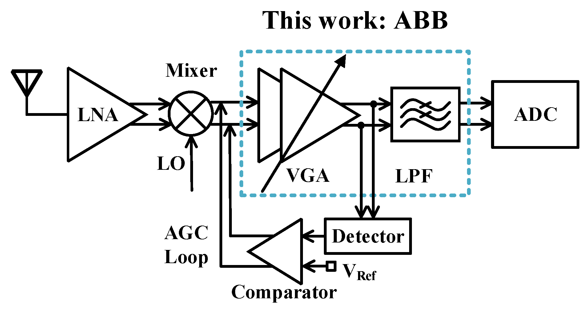
2. Analog Baseband Architecture

Figure 3 illustrates the complete structure of the proposed fully differential wideband dB-linear ABB system, which consists of two variable gain units, a 3-stage fixed gain amplifier (FGA) unit, a 4th-order Butterworth LPF, a DC offset cancellation (DCOC) network, and an output buffer for testing purposes only. The two distinct variable gain units are proposed to achieve wideband and precise dB-linear performance followed by a 3-stage FGA unit for sufficient voltage gain with a DCOC network for the DC offset correction after FGA stage 1. Finally, the filter used the transconductance-capacitance (Gm-C) structure to achieve wideband characteristics, and a 4th-order low-pass Butterworth transfer function is implemented through two cascaded biquadratic cells. For stand-alone RF testing purposes, a 100 Ω resistor is placed across the ABB differential inputs to achieve input impedance matching. Similarly, the output impedance of the output buffer stage is matched to a 100 Ω differential. The output buffer shown in Figure 3 used a simple resistance-loaded common source structure to match the output impedance to a 100 Ω differential.
In general, the overall noise performance of the receiver is primarily determined by the first stage, while the linearity of the system depends on the subsequent stages. Therefore, linearity is the main concern for the ABB design since it is placed at the last stage of the receiver system. The first variable gain unit has low gain due to its wideband and dB-linear characteristics, which result in high linearity. For this reason, unit 1 is positioned at the front end to attenuate the input signal. In contrast, the FGA stage exhibits poor linearity because of its higher gain, so it is placed behind the variable gain unit. A filter is placed at the final stage to minimize noise before the signal reaches the ADC input.

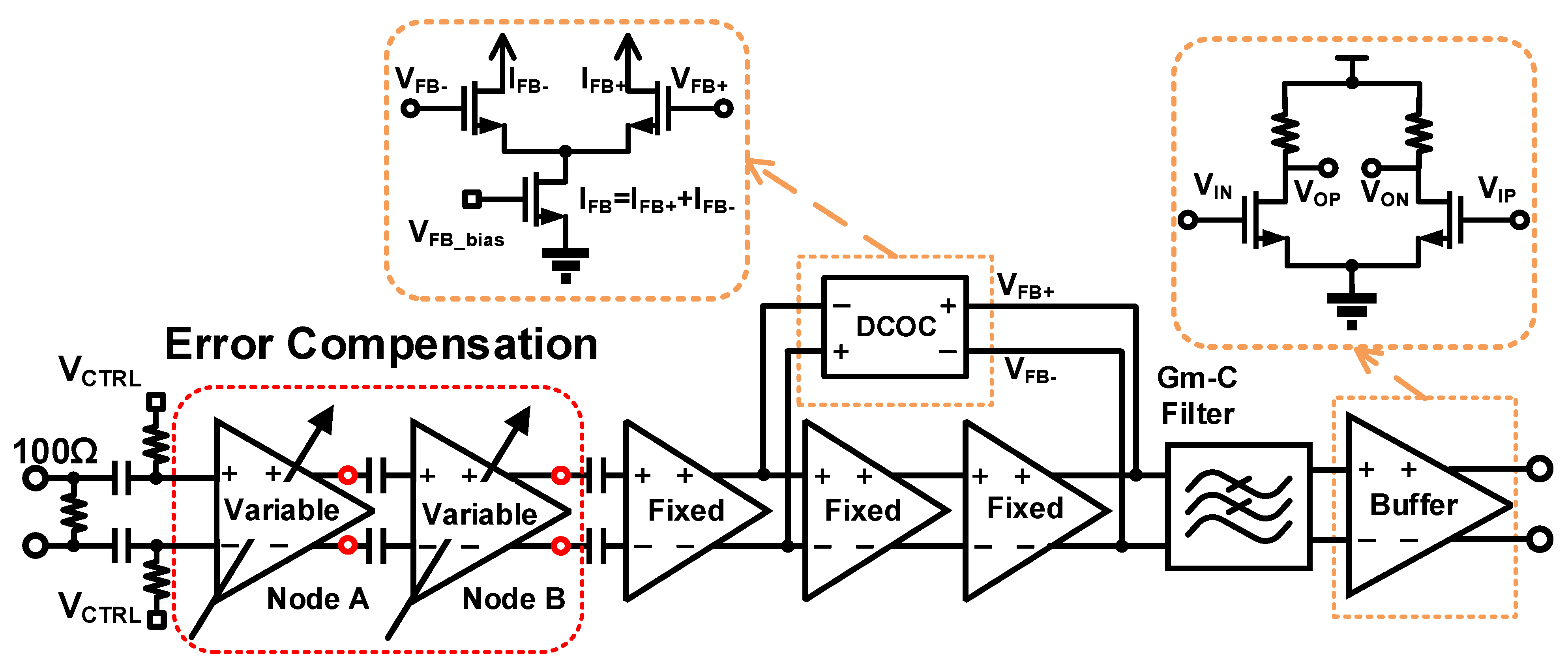
3. Detailed Circuit Designs of the Analog Baseband

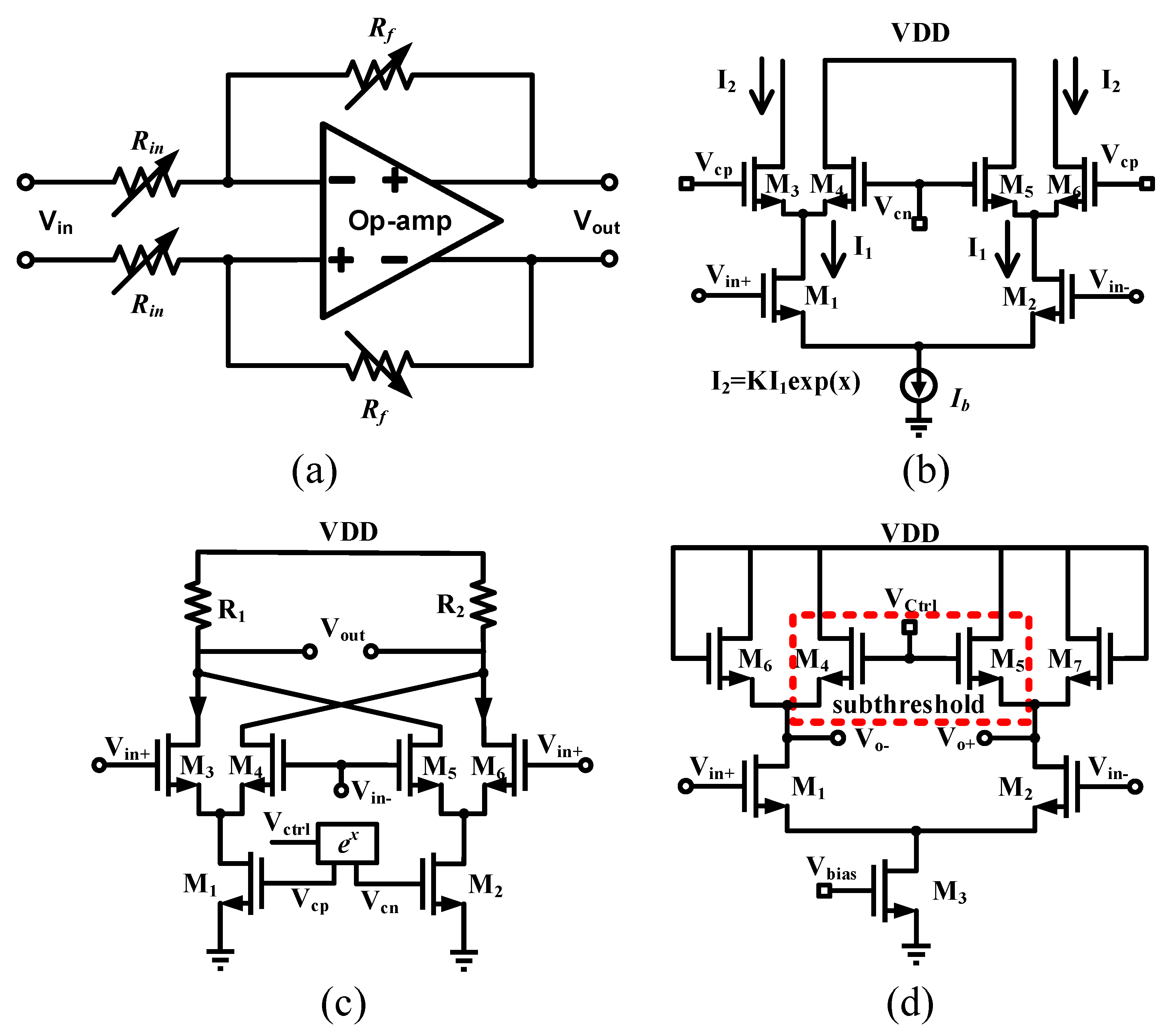
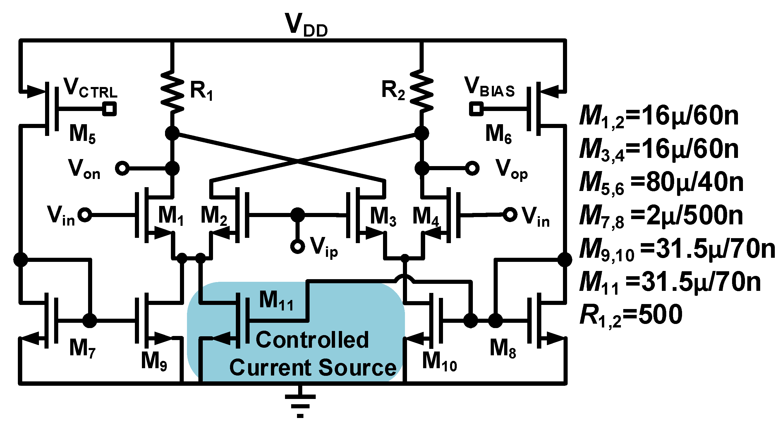
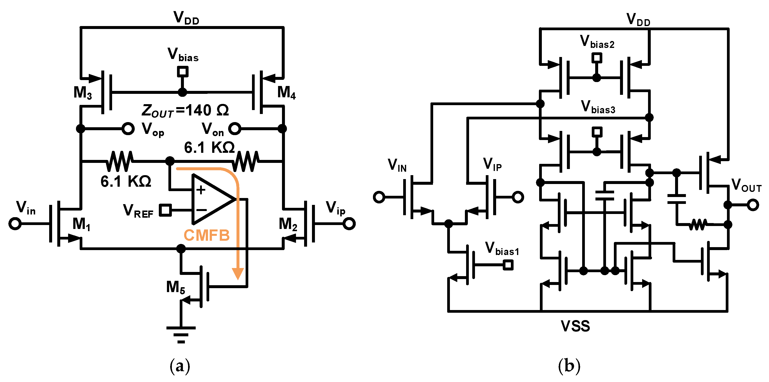
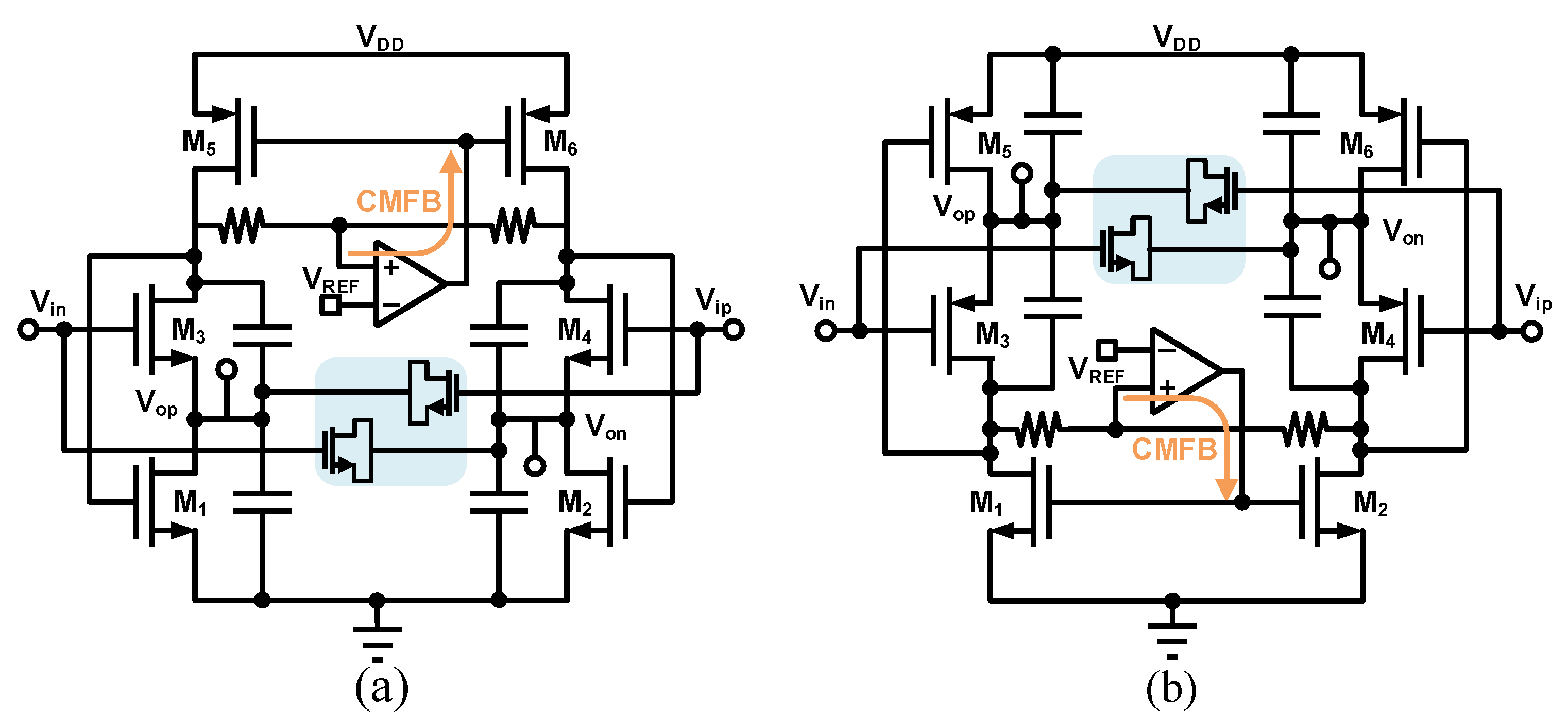
3.1. dB-Linear Variable Gain Unit Core

Figure 4 shows the schematic of core unit 1, which employs a fully differential pair with self-compensated transistors and an active inductor load [31]. The active inductor, realized by a diode-connected transistor with the gate connected to a series resistor, serves as a load to resonate out the output capacitor to extend the bandwidth. Compared to a traditional passive inductor load, the active inductor occupies a compact area without additional power consumption. Figure 4 also shows the inductive output provided by a source follower and its equivalent network. Taking the gate-source parasitic capacitance into consideration, the output impedance seen from the source node of ML can be expressed as [32]:
Z o u t = R S C G S s + 1 / ( g m + C G S s )
Z o u t 1 g m = C G S s ( R S 1 g m ) / ( g m + C G S s )
The output impedance is approximately equal to 1/gm, with CGS acting as an open circuit and ML acting as a diode-connected transistor at low frequency. At high frequency, the output impedance is approximately equal to RS. Then, an inductive behavior can be realized. The output impedance can be modeled as a lossy inductor in series with a resistor, and inductance can be obtained by derivation as
L = C g s g m R S 1 g m
If RS >> 1/gm, the inductance of the active inductor can be given by:
L = R S C g s / g m
Therefore, the value of the inductor can be adjusted by adjusting the value of the resistor and the size of the MOS transistor.
In this design, the differential input pair transistors of M1,2 operate in the triode region instead of saturation, while the tail current source transistor M5 operates in the saturation region, maintaining a constant current flow, which results in a fixed VGS value of transistor M3,4. To maintain a constant current value, the source voltage of M1,2 is adjusted corresponding to the gate voltage of M1,2. Thus, the drain current for the MOS transistor working in the triode region can be given by
I D = K ( V G S V T H V D S 1 2 V D S 2 ]
where K = μ C o x W / L . Thus, V S can be expressed:
V S = V G V T H ± V G V D V T H 2 + 2 I D K
As the overdrive voltage V o v = ( V G V D V T H ) > 0 , only the one with the minus sign is applicable, obtaining
V D S = V G V D V T H + V G V D V T H 2 + 2 I D K
the transconductances of M1,2 can be expressed as follows:
g m 1 , 2 = I D / V G S = K V D S = K V G V D V T H + V G V D V T H 2 + 2 I D K
Thus, it can be simplified in the form of
g m 1 , 2 = A x + x 2 + 1
where A = K / 2 I D / K and x = V G V D V T H / 2 I D / K . According to the Taylor expansion x 2 + 1 1 + x 2 / 2 , the expression for gm can be written as:
g m A e x = A e V G / 2 I D / K × e V D + V T H / 2 I D / K
It is evident that A, K, and VD are constant values. Consequently, this equation can be succinctly expressed as follows:
g m C 1 e V G / 2 I D / K
Given that C 1 = K e V D + V T H / 2 I D / K , the relationship between the gate voltage of the input transistor and its transconductance in dB-linear scale can be obtained. However, because some higher order terms are ignored in the equivalence process, the pseudo-exponential relationship between gm and VG still admits error compared with the ideal exponential function [33]. Meanwhile, output resistance is also a key factor for the dB-linear characteristics. When the differential pair transistors are operating in the triode region, their output resistance can be expressed by the following equation:
r d s 1 = V D S 1 I D = 1 g d s 1 = 1 K V G S V T H V D S = 1 x 2 I D K
Since the load of unit 1 can be simplified as a diode-connected transistor. Consequently, the output resistance of unit 1 can be given by:
R out = 1 g d s 1 + g m 3 = 1 K 3 / K 1 + x 2 I D K 1 = 1 K 1 V C T R L + C 2
where C 2 = 2 I D K 3 / K 1 V D + V T H . From (13), it can be derived that there is an inverse proportion between the gate voltage of the input transistor and the output resistance of unit 1. This inverse relationship is only approximately equivalent to the exponential relationship in a very narrow range, so output resistance will also cause dB-linear gain errors. In [34], the dB-linear gain error caused by the output resistance is reduced through adjusting the value of K3/K1. However, this method still presents significant dB-linear gain errors, especially cascading two identical unit 1s.
To address this issue, this paper presents an error compensation method to achieve lower dB-linear gain error. The schematic of core unit 2 is illustrated in Figure 5 as an improved folding Gilbert unit. In response to the inverse proportionality between the output resistance and control voltage of unit 1, the Gilbert unit with a linear relationship between control voltage and gain is selected to mitigate this inverse proportionality. Moreover, an additional tail current transistor M11 is incorporated into the traditional folding Gilbert structure. This integration introduces a constant term into the over gain expression, contributing to an improved error compensation for dB-linear gain. The over gain expression of the improved folding Gilbert unit can be expressed as follows:
A v = G m R L = C 3 V C T R L C 4  
where C 3 = R 1 , 2 K 1 , 3 K 9 , 10 / 2 ( W / L ) 5 , 6 / ( W / L ) 7 , 8 and C 4 = ( W / L ) 11 / ( W / L ) 8 V V D D V B i a s V T H 6 + V B i a s . Based on Equations (11), (13) and (14), the gain expression of cascade of unit 1 and unit 2 (Node B in Figure 3) can be expressed as follows:
A t o t a l C 1 e V G / 2 I D / K K 1 V C T R L + C 2 × C 3 V C T R L C 4
where V G = V C T R L . By adjusting the size of transistor M11 in unit 2 to keep C2 = −C4, the gain expression can be expressed as follows:
A t o t a l C 1 C 3 e V C T R L / 2 I D / K K 1
As can be seen from (16), C1, C3, ID, and K are constant terms, so the VGA control voltage VCTRL and the overall gain A t o t a l present a dB-linear relationship with error compensation.
From (10), the dB-linear error stemming from the output impedance of unit 1 can be compensated, and the overall gain exhibits a dB-linear relationship with the control voltage. To optimize error compensation in the proposed design, the gain characteristics of unit 1 (Node A in Figure 3) remain constant. Subsequently, the gain characteristics of unit 2 and cascaded unit 1 and 2 (VGA_cascade, Node B in Figure 3) are simulated with different widths of M11. The simulation results of the gain characteristics shown in Figure 6a and the gain error results shown in Figure 6b, indicate that the optimal error compensation effect can be achieved when the width of M11 is set to 31.5 μm. Then the gain range of unit 1 is about –18~4 dB, and the gain range of optimized unit 2 is about –19~4 dB. The gain range of the VGA_cascade is about –38~7 dB after compensation and the dB-linear error of the optimized VGA_cascade is only ±0.3 dB.
In order to verify the effectiveness of the proposed error compensation method, the gain range and the gain error were simulated with and without the error compensation method (without error compensation is a cascade of two unit 1 stages). Figure 7a shows the simulated gain curve and the ideal gain curve with and without the proposed error compensation method, and a more obvious dB-linear relationship can be seen in the gain curve with the compensation method. Figure 7b shows the dB-linear gain error with and without the proposed error compensation method. The simulation result without the error compensation method shows that the dB-linear gain error reaches ±1.8 dB, while the dB-linear gain with the error compensation method is reduced to ±0.3 dB—an improvement of more than 80%. In comparison, even the optimized two-stage unit 1 cascade in [34] results in a dB-linear gain error of ±1 dB. These results demonstrate that the proposed error compensation method effectively minimizes the dB-linear gain error within a gain range of 45 dB.
The gain control mechanism of the dB-linear system can be severely hampered by circuit mismatches and PVT variations. In order to verify the robustness of the proposed dB-linear VGA, PVT and Monte Carlo simulations are performed. Figure 8 shows the dB-linear gain error at different process corners (TT, FF, SS, SF, and FS), at temperatures of (–40 °C, 27 °C, and 125 °C), and at power supply voltages under ±10% fluctuation: 0.9 V, 1 V, and 1.1 V, respectively. It can be observed that the dB-linear gain error exhibits small variation, maintaining itself within ±1 dB with the variations of temperatures or process corners. In addition, the dB-linear gain error is still within the ±1.5 dB range even under extreme conditions where both process corners, temperatures, and power supply voltages vary simultaneously.
To further verify the effects of process corners and mismatches, Monte Carlo simulations were performed. A total of 100 random simulations were performed at a normal power supply voltage (1 V) and temperature (27 °C) and the same bias voltage environment as before. Figure 9a shows the dB-linear gain error curve obtained by 100 random simulations. It can be seen that the most of dB-linear gain error is within ±1 dB, and the maximum dB-linear gain error is ±1.4 dB. Figure 9b shows the normal distribution statistics of the maximum dB-linear gain error obtained by 100 simulations. It can be seen that 72% of the time the maximum dB-linear gain error is less than ±0.5 dB, and 92% of the time the maximum dB-linear gain error is less than ±1 dB with an average maximum gain error of 0.392 dB and a standard deviation of 0.306 dB.

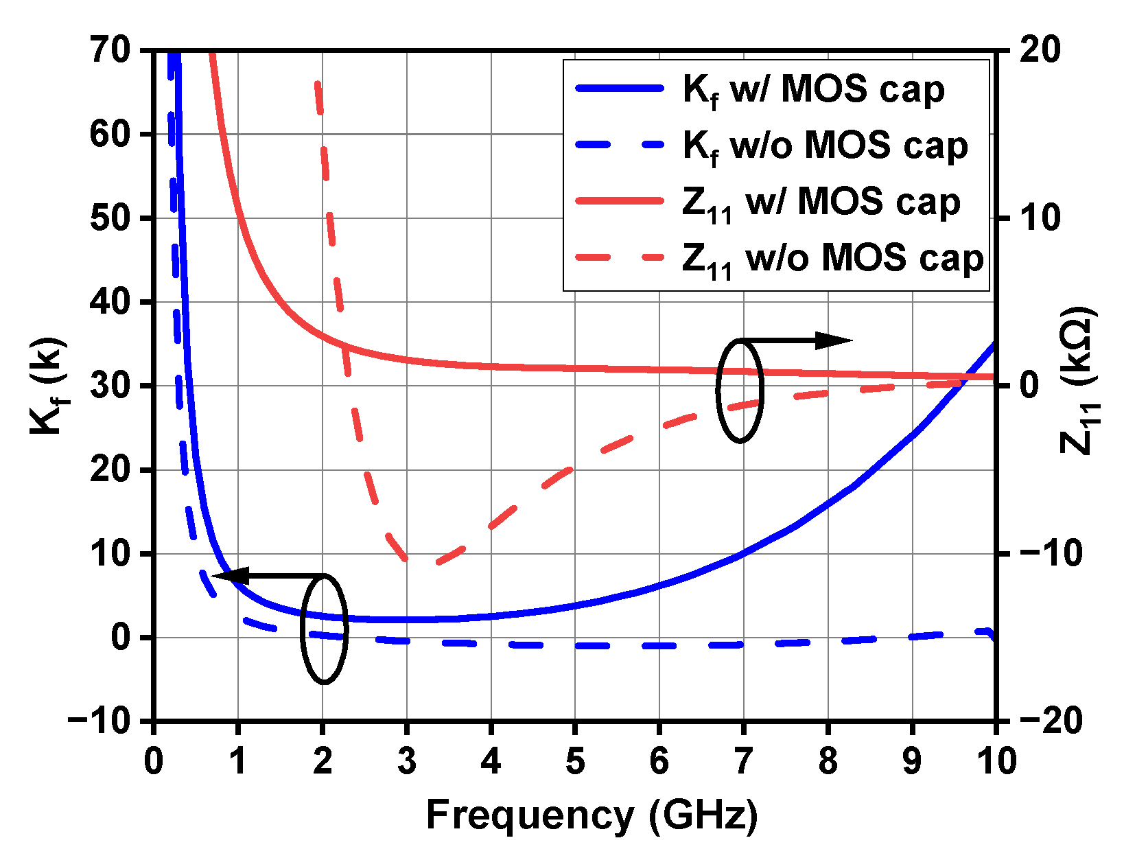
3.2. Fixed Gain Amplifier

As depicted in Figure 6, the gain of VGA_cascade primarily exhibits negative characteristics owing to its wideband and dB-linear characteristics. Therefore, cascading several FGA units is necessary to achieve enough gain. If each FGA unit is identical and has a bandwidth of BWc, the overall bandwidth of n cascaded stages BWtot is [35]:
B W t o t = B W c 2 1 / n 1 m
where m is equal to 2 for 1st-order stages. The gain of each FGA stage is defined as Ac in dB and Atot is for the total gain. Then, the required gain-bandwidth product GBWc (dB·GHz) of each FGA stage can be written as:
G B W c = G B W t o t n × 2 1 / n 1 m
If Atot = 30 dB and BWtot = 4 GHz represent the design requirements for a cascade of n first-order gain stages, the Ac, BWc, and GBWc are as shown in Table 2.
It can be seen that higher the cascaded stages, the fewer the gain bandwidth product requirements. Therefore, taking the trade-off between the gain and accumulation of noise into account, three stages are selected as the optimum FGA stage to achieve the desired overall gain and bandwidth. Figure 10a depicts the topology of the FGA stage where the fully differential pair with the PMOS current source as the active load is employed. Additionally, a common mode feedback (CMFB) circuit is integrated to ensure the stability of the output DC point. The schematic diagram of the CMFB circuit is shown in Figure 10b, and it adopts a two-stage operational amplifier with folded cascade structure.
The three-stage FGA uses the same design and fixes the output common-mode voltage at 0.7 V via the CMFB circuit. The frequency response of the FGA is shown in Figure 11, and it can be seen that each stage of FGA can provide a gain of 11.7 dB with a 13 GHz bandwidth.

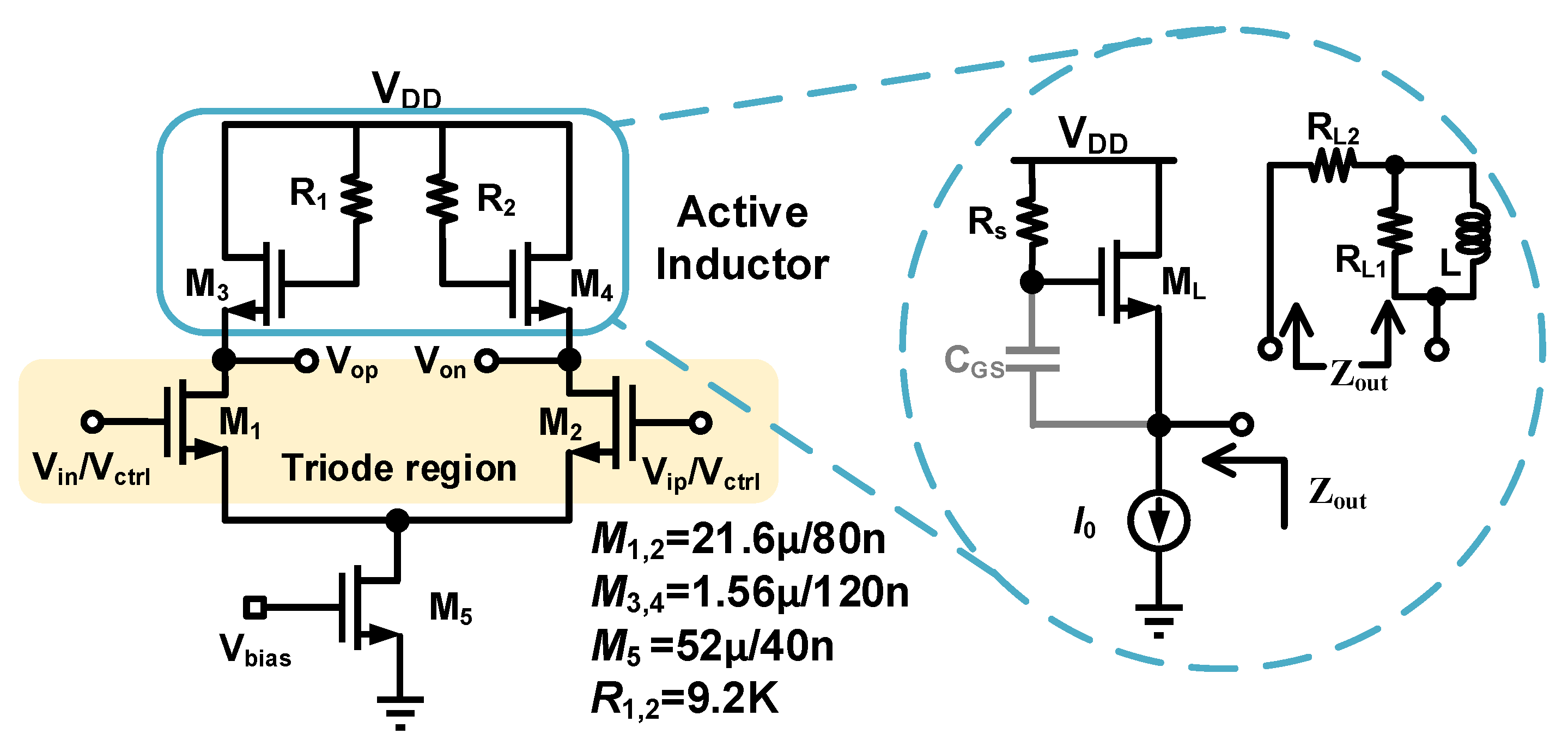
3.3. Low-Pass Filter

To enhance OOB noise rejection in mmW communication systems, the ABB system utilized a 4th-order Butterworth LPF. The filter is composed by the cascade of two biquadratic cells [36]. The cascade alternates NMOS and PMOS type inputs, restoring the input/output common mode voltage. The first cell utilizes a NMOS, achieving a lower quality factor (Q = 0.504). This configuration provides sharp filtering of the input signal, effectively attenuating high-frequency components at the input of the second cell, which exhibits a higher quality factor (Q = 1.307). As a result, this design enhances in-band linearity, albeit at the expense of a slight increase in in-band integrated noise. The topology of the 1st NMOS biquadratic cell and 2nd PMOS biquadratic cell are depicted in Figure 12.
The biquadratic cell utilizes a pseudo-differential structure and the flipped source follower (FSF) structure as the transconductance stage to enhance linearity. FSF incorporates local negative feedback based on the traditional source follower, thus endowing it with higher linearity. The output resistance of the FSF structure can be written as:
Z o u t = r o 2 g m 1 g m 2 r o 1 r o 2 + g m 2 r o 2 + 1 1 g m 1 g m 2 r o 1
Compared to the output resistance of a source follower, the output resistance of the FSF is reduced, resulting in stronger load-driving. The transfer function of the FSF cell can be written as [37]:
T s 1 s 2 C 1 C 2 g m 1 g m 2 + s C 1 g m 1 + 1
The frequency characteristic and quality factor of the filter are written as:
ω n g m 1 g m 2 / C 1 C 2  
Q g m 1 C 2 / g m 2 C 1
Based on the required cutoff frequency and Q value, design-related parameters can be calculated. The frequency response of the LPF is shown in Figure 13, indicating that the loss of LPF is only –3.5 dB, and its bandwidth reaches 5 GHz.
When the operating frequency reaches several GHz, the Cgs of the input transistor would affect the stability of the system. Therefore, the neutralization capacitor technique is employed to enhance the stability of the filter. Figure 14 compares the Z11 and Kf with and without MOS neutralization capacitors, where it can be seen that the Z11 and Kf of the filter become more stable with MOS neutralization capacitors.

3.4. DCOC Network

Due to variations in the output DC operating point of the VGA unit caused by gain adjustments, the AC coupling is employed to establish the correct DC operating point, as illustrated in Figure 3. The output DC voltage of unit 1 varies between 70 mV and 140 mV, and the output DC voltage of unit 2 varies between 640 mV and 945 mV. In the FGA stage, the output common mode point aligns with the input common mode point, allowing for direct cascading. To mitigate the effects of DC offset, a DCOC network is implemented. This DCOC network not only eliminates DC offset but also provides active negative feedback, thereby extending the bandwidth simultaneously [38]. By adjusting the voltage of VFB_bias as shown in Figure 3, the intensity of the active feedback can be regulated to achieve a balance between the bandwidth and gain flatness. The influence of different feedback intensities on the frequency response is shown in Figure 15. As VFB_bias increases from 450 mV to 550 mV, the gain gradually decreases, while the bandwidth gradually increases, resulting in the emergence of a gain peak. Therefore, 500 mV is chosen as the value of VFB_bias by trade off the gain and bandwidth.

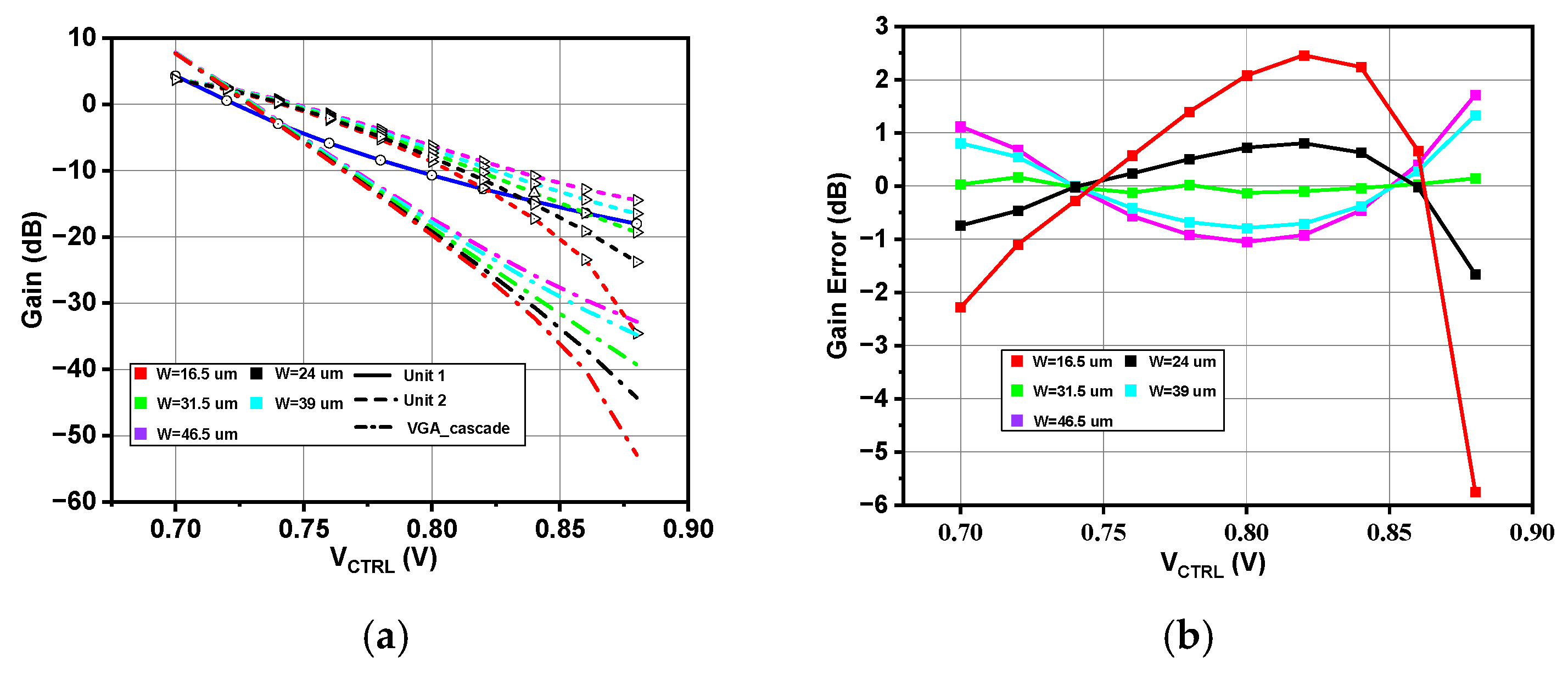
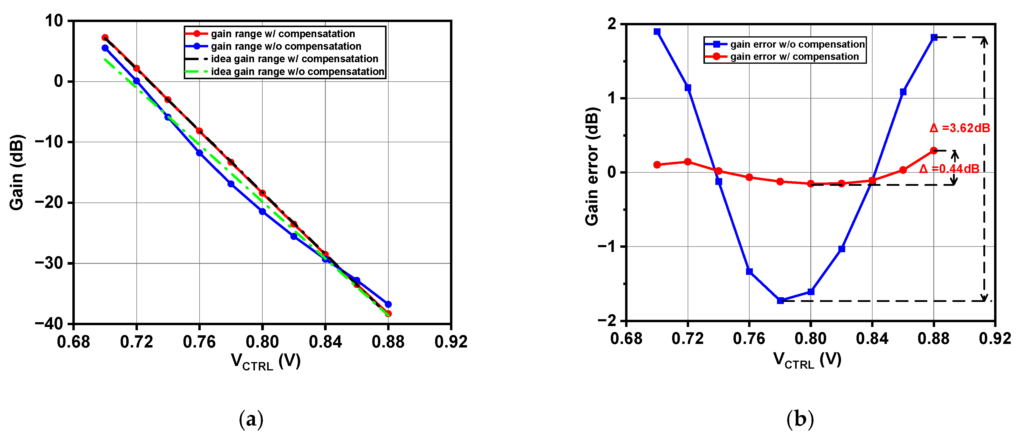
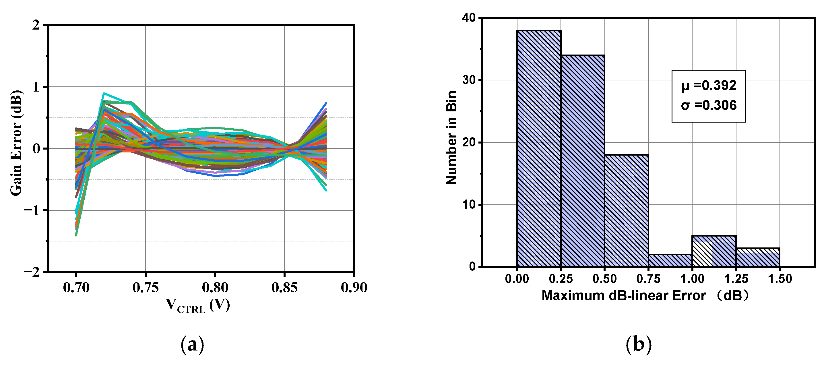
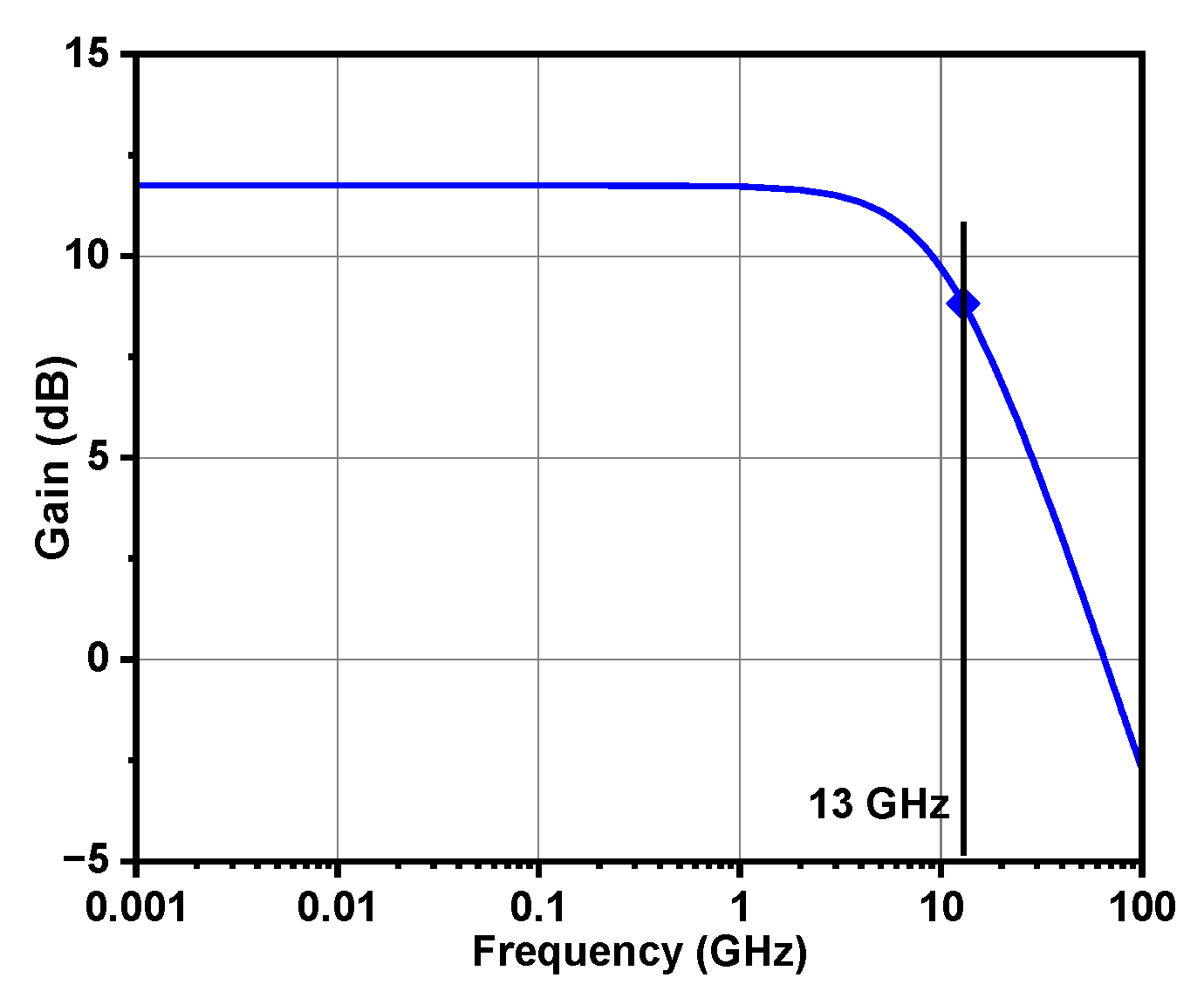
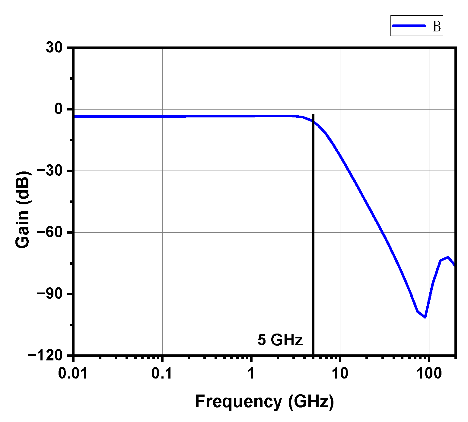
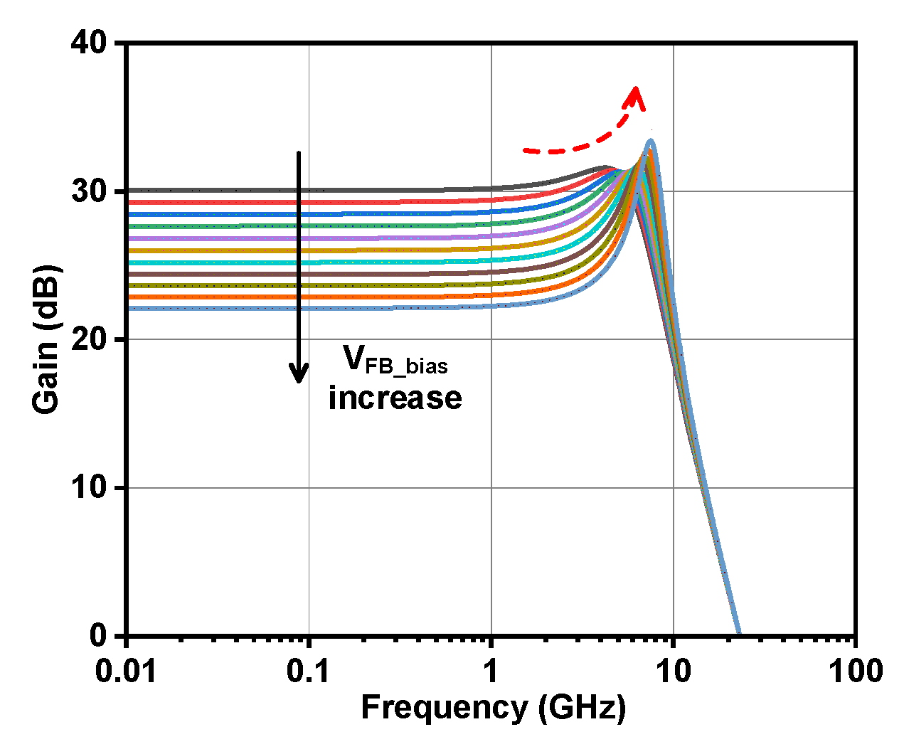
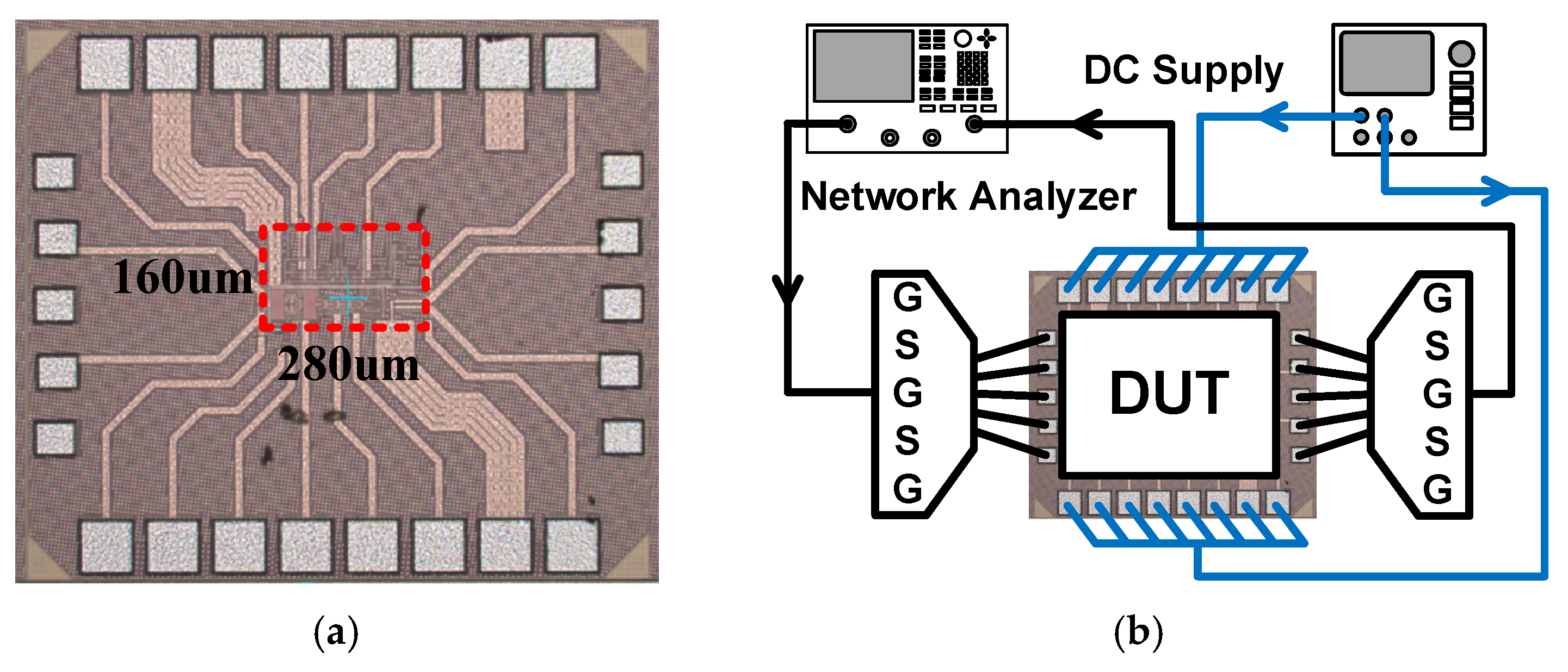
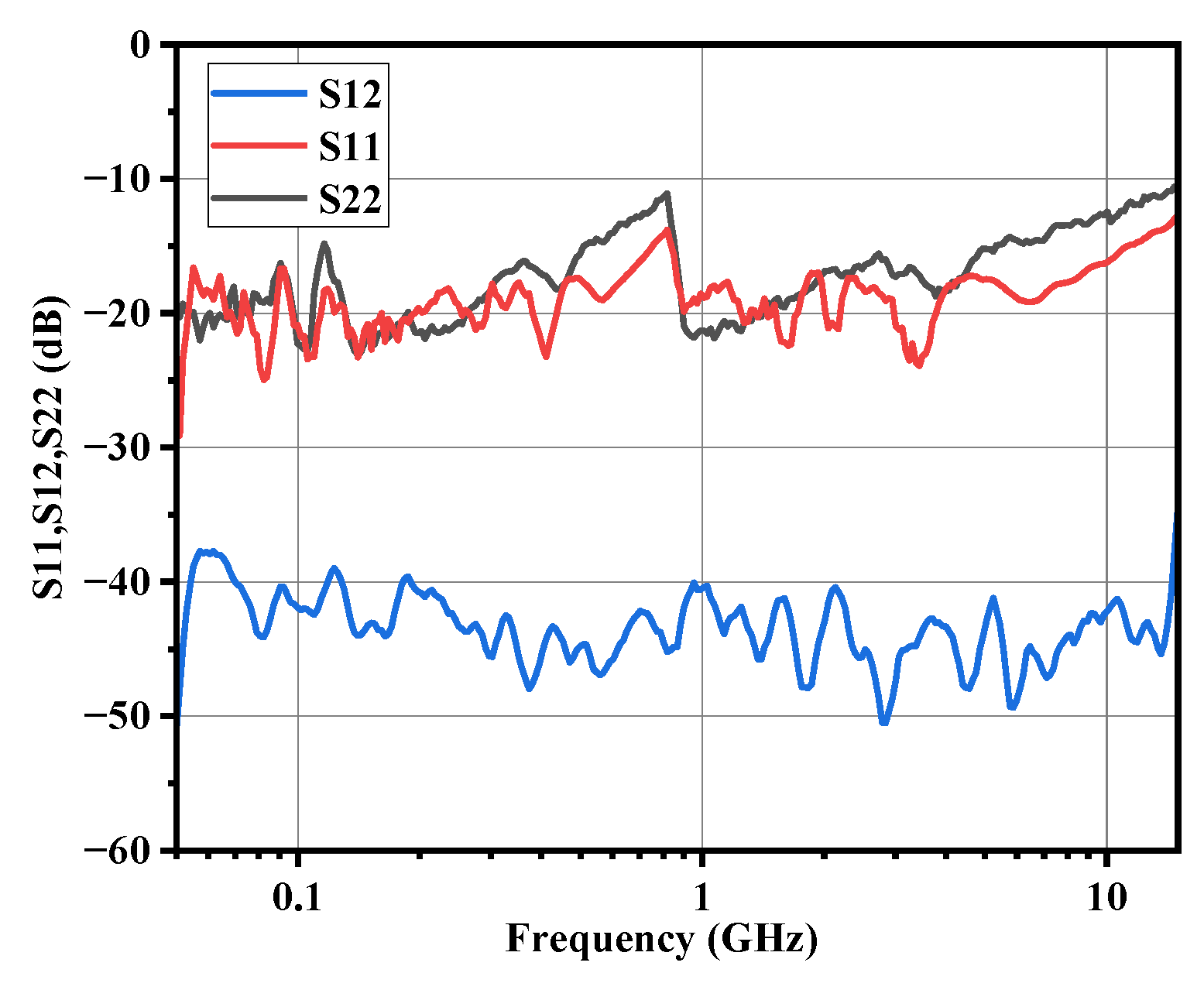
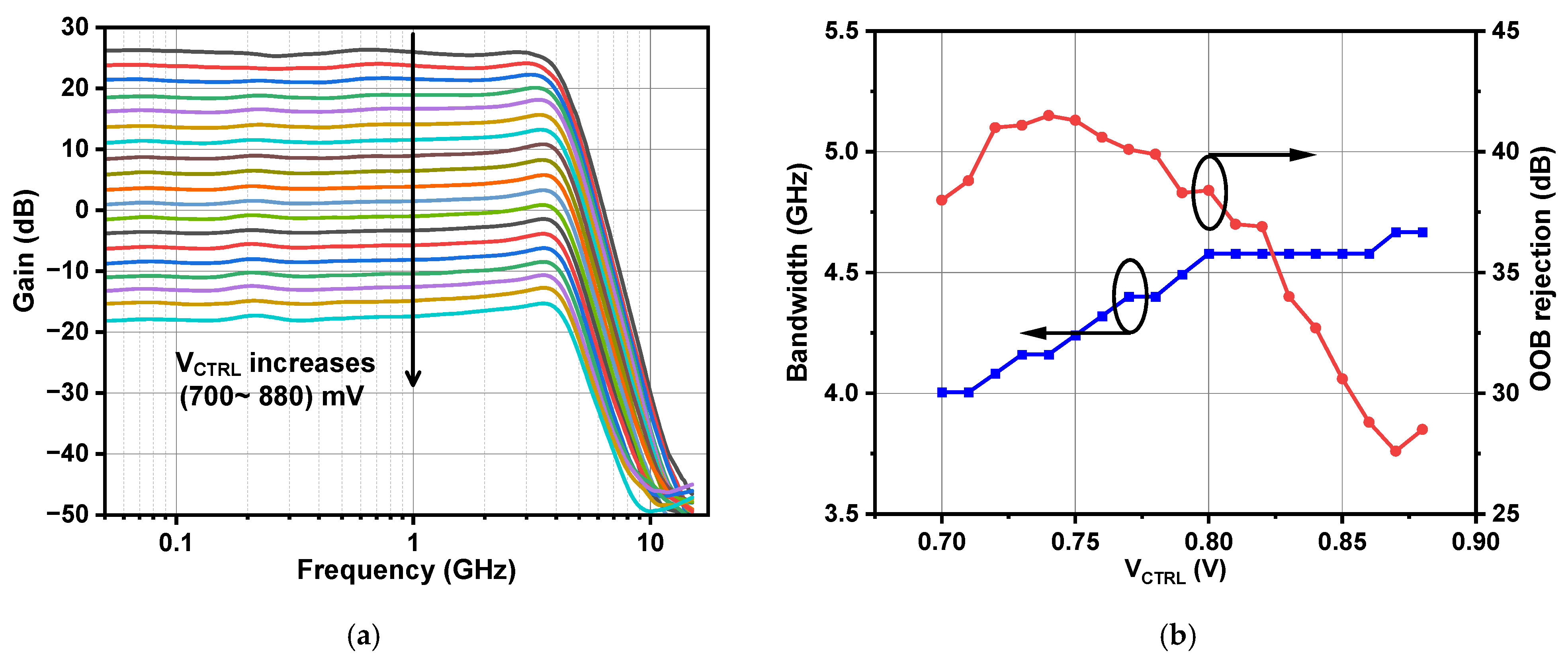
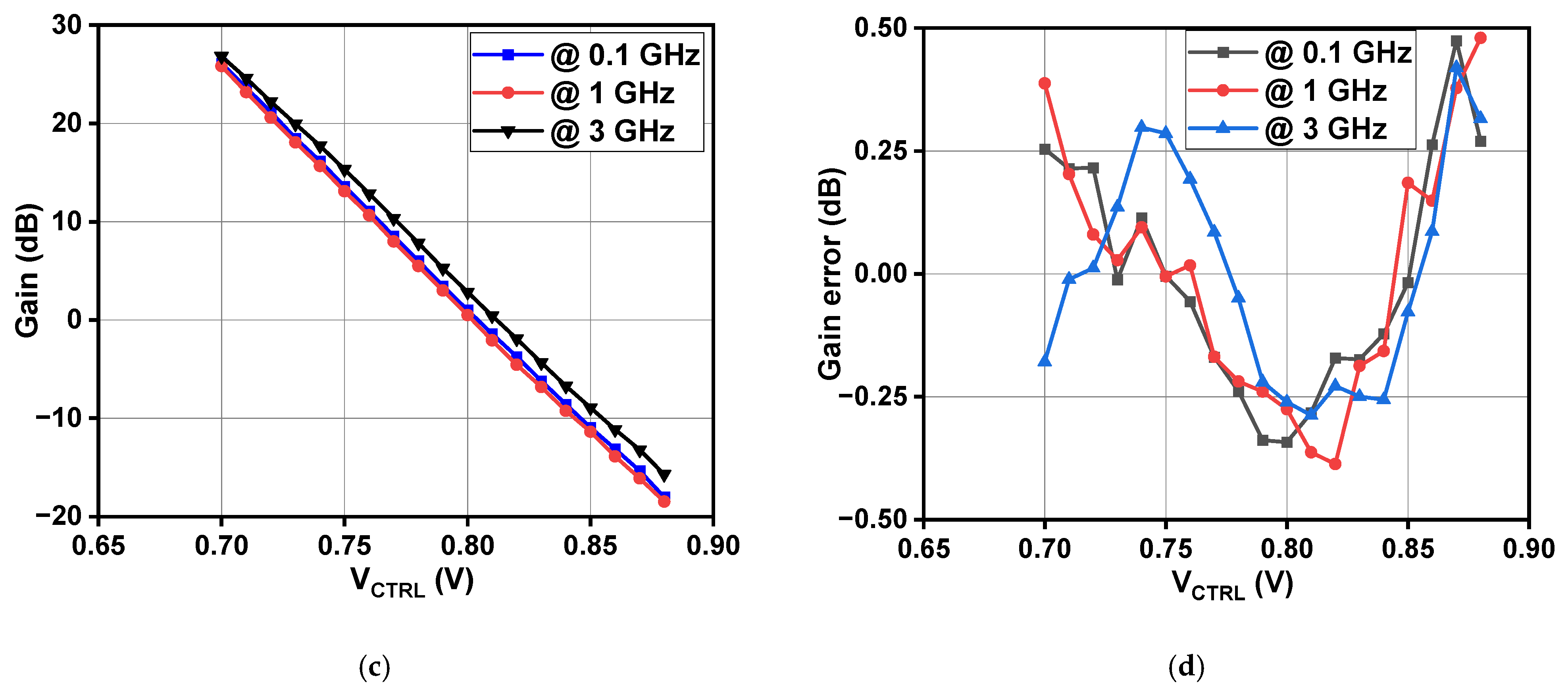
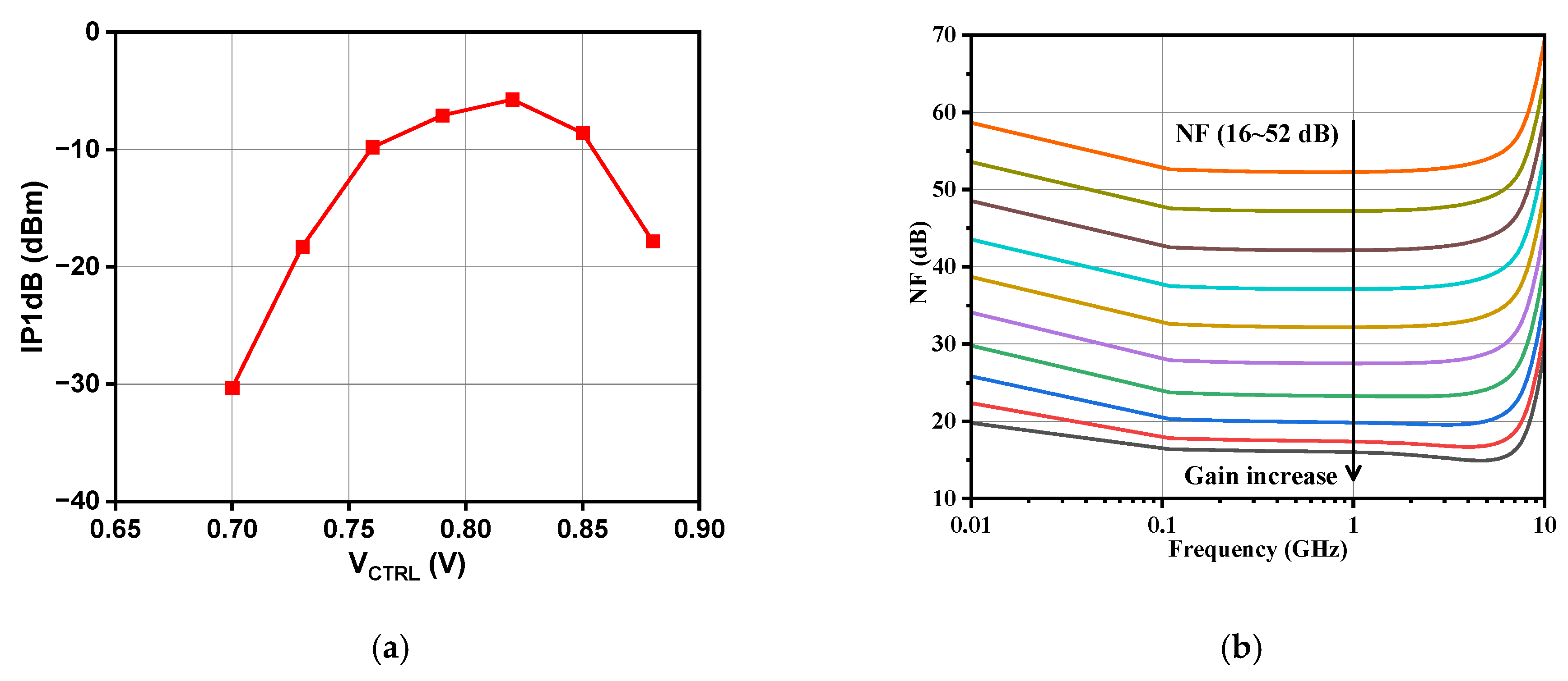
4. Results and Discussion

The proposed ABB prototype was fabricated in 40 nm CMOS technology and tested by wafer probing. Figure 16a shows the chip microphotograph, and the measurement setup is shown in Figure 16b. The ABB system occupies an active area of only 0.045 mm2, while the area of VGA is confined to just 0.027 mm2.
The input and output of the chip are connected to the Keysight network analyzer (N5247B) through the differential probes, and the DC pad is connected to the PCB through wire bonding. The power supply voltage and bias voltage are provided through the DC power supply. All measurements results were performed at room temperature. The measured S11, S22, and S12 (under VCTRL = 700 mV and –50 dBm input power) are shown in Figure 17. It can be seen that S11, S22, and S12 are all less than –10 dB in the range of 0–10 GHz. Therefore, the measured S21 can be used to indicate the gain of the VGA. The frequency response (S21) under different control voltages is also tested by Keysight network analyzer, as shown in Figure 18a (under –50 dBm input power). As the control voltage increases from 700 mV to 880 mV, the gain of the ABB system decreases. Figure 18b shows that the bandwidth of the ABB system increases from 4 GHz to 4.6 GHz as the control voltage increases, and its OOB rejection function provided by the filter is also verified as there is more than a 25 dB attenuation at twice the bandwidth frequency. The ABB system achieves a dB-linear gain variation range of 44 dB from 26 dB to –18 dB. Figure 18c,d summarizes the dB-linear gain range and dB-linear gain error at different frequencies. It can be seen that the ABB system has an excellent dB-linear characteristic within the dB-linear gain range of 44 dB (26 dB to –18 dB), and the dB-linear gain error is calculated to be less than ±0.5 dB.
With the provided power supply and bias voltage, the gain of the chip at 1 GHz under the input power of −50~0 dBm is scanned by the network analyzer with different control voltages to measure the IP1dB of the chip. Figure 19a displays the IP1dB results at 1 GHz of ABB system under different control voltages, ranging from –30 dBm to –5.7 dBm. In the high gain mode, the output swing exceeds the maximum allowable range, resulting in a limited IP1dB, and it can be seen that IP1dB increases as the gain decreases. However, when the input signal reaches a certain level, it becomes saturated before the output signal, resulting in the reduction of IP1dB [34]. Figure 19b presents the NF simulation results of the ABB system. It can be seen that the NF of ABB at 1 GHz is 16 dB at the highest gain, while the NF at the lowest gain is 52 dB.
Table 3 presents the comparison between this work and other ABB systems. It can be seen that, compared to other ABB systems, the proposed ABB system achieves a significant bandwidth improvement while maintaining low power consumption, thanks to the use of the active inductor technique. Additionally, the system achieves better dB-linear characteristics through the proposed self-compensated transistor technique and the error compensation method.
Table 4 presents the comparison between this work and other state-of-the-art works. Based on [39], a modified Figure of Merit (FOM) is given by:
F O M = d B l i n e a r   G a i n   R a n g e d B × B W G H z P o w e r m W × A r e a m m 2 × G a i n   e r r o r d B
The VGAs in [10,27] offer a wide dB-linear gain range and a low dB-linear gain error but lack the bandwidth required for mmW communication applications. In contrast, the VGAs proposed in [9,22,23] provide sufficient bandwidth for mmW communication applications but rely on additional exponential generator circuits, increasing power consumption and circuit complexity. The proposed VGA achieves excellent wideband dB-linear characteristics without using additional exponential generator circuits because of the designed active inductor technique and self-compensating transistor technique, and its power consumption and area are well improved. Compared to the VGA in [34], the VGA proposed in this paper achieves a 10% improvement in dB-linear gain range and a 50% reduction in dB-linear gain error while maintaining the same bandwidth due to the proposed error compensation method. The proposed error compensation method effectively reduces the dB-linear gain error of the VGA, and can be utilized in a high-precision AGC loop to improve the accuracy of signal processing with high dynamic range. However, due to the triode mode operation of the differential pair transistors of the first-stage VGA instead of the saturation region, the linearity is largely affected, resulting in limitations for RF receivers in applications with high linearity requirements.

5. Conclusions

A compact wideband dB-linear multi-cascaded stage ABB circuit using several unique techniques for gain error correction, linearity, and stability enhancement is presented in this paper. The self-compensated transistor pair with an area-efficient active inductor is designed to realize the wideband dB-linear function in the first VGA unit, followed by second VGA unit which employs a proposed error compensation method for the dB-linear gain error correction enhancement. Moreover, an FSF structure is employed to enhance the linearity of the Gm-C LPF between the VGA and output buffer for testing purposes only, and the stability of the filter is secured by neutralization technique. The ABB prototype was fabricated in 40 nm low power (LP) CMOS technology and tested. The measurement results demonstrated that, thanks to the proposed compensation method, the ABB system achieves the state-of-the-art high precision dB-linear characteristics with a dB-linear gain error of less than 0.5 dB in the whole gain tuning range of 44 dB, and its bandwidth reaches 4 GHz with a compact size of 0.045 mm2 and low power consumption under 1 V DC supply.

Author Contributions

Conceptualization, S.H.; methodology, S.H. and H.W.; software, S.H.; validation, S.H.; formal analysis, S.H. and H.W.; investigation, S.H.; resources, S.H.; data curation, S.H.; writing—original draft preparation, S.H. and H.W.; writing—review and editing, Y.W.; visualization, S.H.; supervision, Y.W.; project administration, Y.W.; funding acquisition, Y.W. All authors have read and agreed to the published version of the manuscript.

Funding

This work was funded by the Fundamental Research Funds for the Central Universities under Grant 2020ZYGXZR067.

Data Availability Statement

Data are contained within the article.

Conflicts of Interest

The authors declare no conflicts of interest.

References

  1. Doan, C.H.; Emami, S.; Niknejad, A.M.; Brodersen, R.W. Design of CMOS for 60GHz applications. In Proceedings of the 2004 IEEE International Solid-State Circuits Conference (IEEE Cat. No.04CH37519), San Francisco, CA, USA, 15–19 February 2004; pp. 440–441. [Google Scholar] [CrossRef]
  2. Doan, C.H.; Emami, S.; Niknejad, A.M.; Brodersen, R.W. Millimeter-wave CMOS design. IEEE J. Solid-State Circuits 2005, 40, 144–155. [Google Scholar] [CrossRef]
  3. Ghittori, N.; Vigna, A.; Malcovati, P.; D’Amico, S.; Baschirotto, A. A 1.2-V 30.4-dBm OIP3 Reconfigurable Analog Baseband Channel for UMTS/WLAN Transmitters. IEEE Trans. Circuits Syst. I Regul. Pap. 2006, 53, 2125–2131. [Google Scholar] [CrossRef]
  4. Siligaris, A.; Richard, O.; Martineau, B.; Mounet, C.; Chaix, F.; Ferragut, R.; Dehos, C.; Lanteri, J.; Dussopt, L.; Yamamoto, S.D.; et al. A 65-nm CMOS Fully Integrated Transceiver Module for 60-GHz Wireless HD Applications. IEEE J. Solid-State Circuits 2011, 46, 3005–3017. [Google Scholar] [CrossRef]
  5. Kulkarni, R.; Kim, J.; Jeon, H.-J.; Xiao, J.; Silva-Martinez, J. UHF Receiver Front-End: Implementation and Analog Baseband Design Considerations. IEEE Trans. Very Large Scale Integr. (VLSI) Syst. 2012, 20, 197–210. [Google Scholar] [CrossRef]
  6. Liao, C.-F.; Liu, S.-I. A 10Gb/s CMOS AGC Amplifier with 35dB Dynamic Range for 10Gb Ethernet. In Proceedings of the 2006 IEEE International Solid State Circuits Conference-Digest of Technical Papers, San Francisco, CA, USA, 6–9 February 2006; pp. 2092–2101. [Google Scholar] [CrossRef]
  7. He, L.; Li, L.; Wu, X.; Wang, Z. A Low-Power Wideband dB-Linear Variable Gain Amplifier With DC-Offset Cancellation for 60-GHz Receiver. IEEE Access 2018, 6, 61826–61832. [Google Scholar] [CrossRef]
  8. Liu, C.; Yan, Y.-P.; Goh, W.-L.; Xiong, Y.-Z.; Zhang, L.-J.; Madihian, M. A 5-Gb/s Automatic Gain Control Amplifier With Temperature Compensation. IEEE J. Solid-State Circuits 2012, 47, 1323–1333. [Google Scholar] [CrossRef]
  9. Kong, L.; Chen, Y.; Boon, C.C.; Mak, P.-I.; Martins, R.P. A wideband inductorless dB-linear automatic gain control amplifier using a single branch negative exponential generator for wireline applications. IEEE Trans. Circuits Syst. I Reg. Pap. 2018, 65, 3196–3206. [Google Scholar] [CrossRef]
  10. Cai, L.; Song, X.; Lu, Z.; Yu, X.P.; Yeo, K.S.; Chen, J.M.; Thangarasu, B.K. A Linear-in-Decibel Automatic Gain Control Amplifier With Dual Mode Continuous Gain Tuning. IEEE Trans. Circuits Syst. I Reg. Pap. 2023, 70, 2752–2761. [Google Scholar] [CrossRef]
  11. Thangarasu, B.K.; Ma, K.; Yeo, K.S. A 0.029 mm2 8 Gbit/s current-mode AGC amplifier with reconfigurable closed-loop control in 65 nm CMOS. In Proceedings of the 2017 IEEE MTT-S International Microwave Symposium (IMS), Honololu, HI, USA, 4–9 June 2017; pp. 107–110. [Google Scholar] [CrossRef]
  12. Wang, Y.; Ye, L.; Liao, H.; Huang, R.; Wang, Y. Highly Reconfigurable Analog Baseband for Multistandard Wireless Receivers in 65-nm CMOS. IEEE Trans. Circuits Syst. II Express Briefs 2015, 62, 296–300. [Google Scholar] [CrossRef]
  13. D’Amico, S.; Spagnolo, A.; Donno, A.; Chironi, V.; Wambacq, P.; Baschirotto, A. A Low-Power Analog Baseband Section for 60-GHz Receivers in 90-nm CMOS. IEEE Trans. Microw. Theory Tech. 2014, 62, 1724–1735. [Google Scholar] [CrossRef]
  14. Wang, Y.; Hull, C.; Murata, G.; Ravid, S. A linear-in-dB analog baseband circuit for low power 60GHz receiver in standard 65nm CMOS. In Proceedings of the 2013 IEEE Radio Frequency Integrated Circuits Symposium (RFIC), Seattle, WA, USA, 2–4 June 2013; pp. 225–228. [Google Scholar] [CrossRef]
  15. Miyahara, M.; Sakaguchi, H.; Shimasaki, N.; Matsuzawa, A. An 84 mW 0.36 mm2 analog baseband circuits for 60 GHz wireless transceiver in 40 nm CMOS. In Proceedings of the 2012 IEEE Radio Frequency Integrated Circuits Symposium, Montreal, QC, Canada, 17–19 June 2012; pp. 495–498. [Google Scholar] [CrossRef]
  16. Fan, C.; Chen, Z.; Liu, Z.; Li, X.; Li, X.; Qi, Q.; Gu, W.; Wang, X. Design of a Wideband dB-Linear Variable Gain Amplifier With Continuous Gain Adjusting in 90-nm CMOS Technology. IEEE Access 2021, 9, 152646–152656. [Google Scholar] [CrossRef]
  17. Dong, Y.; Kong, L.; Boon, C.C.; Yang, K.; Liu, Z.; Li, C.; Zhou, A. A Wideband dB-Linear Variable-Gain Amplifier With a Compensated Negative Pseudo-Exponential Generation Technique. IEEE Trans. Microw. Theory Tech. 2021, 69, 2809–2821. [Google Scholar] [CrossRef]
  18. Ray, S.; Hella, M.M. A 10 Gb/s inductorless AGC amplifier with 40 dB linear variable gain control in 0.13 μm CMOS. IEEE J. Solid State Circuits 2016, 51, 440–456. [Google Scholar] [CrossRef]
  19. Liu, H.; Boon, C.C.; He, X.; Zhu, X.; Yi, X.; Kong, L.; Heimlich, M.C. A wideband analog-controlled variable-gain amplifier with dB-linear characteristic for high-frequency applications. IEEE Trans. Microw. Theory Tech. 2016, 64, 533–540. [Google Scholar] [CrossRef]
  20. Elwan, H.; Tekin, A.; Pedrotti, K. A Differential-Ramp Based 65 dB-Linear VGA Technique in 65 nm CMOS. IEEE J. Solid-State Circuits 2009, 44, 2503–2514. [Google Scholar] [CrossRef]
  21. Baghtash, H.F. A 37-μW, binary-weighted PGA based on a novel degeneration transistor-ladder. IEEE Trans. Circuits Syst. II Exp. Briefs 2018, 65, 36–40. [Google Scholar] [CrossRef]
  22. Wang, L.-S.; Ku, P.-C.; Ko, P.-T.; Chung, C.-J.; Lu, L.-H. A 40.4-dB range, 0.73-dB step, and 0.07-dB error programmable gain amplifier using gain error shifting technique. IEEE Trans. Circuits Syst. II Exp. Briefs 2019, 66, 1109–1113. [Google Scholar] [CrossRef]
  23. Kumar, T.B.; Ma, K.; Yeo, K.S. A 7.9-mW 5.6-GHz Digitally Controlled Variable Gain Amplifier With Linearization. IEEE Trans. Microw. Theory Tech. 2012, 60, 3482–3490. [Google Scholar] [CrossRef]
  24. Kang, S.-Y.; Ryu, S.-T.; Park, C.-S. A Precise Decibel-Linear Programmable Gain Amplifier Using a Constant Current-Density Function. IEEE Trans. Microw. Theory Tech. 2012, 60, 2843–2850. [Google Scholar] [CrossRef]
  25. Yamaji, T.; Kanou, N.; Itakura, T. A temperature-stable CMOS variable-gain amplifier with 80-dB linearly controlled gain range. IEEE J. Solid-State Circuits 2002, 37, 553–558. [Google Scholar] [CrossRef]
  26. Lee, H.D.; Lee, K.A.; Hong, S. A Wideband CMOS Variable Gain Amplifier With an Exponential Gain Control. IEEE Trans. Microw. Theory Tech. 2007, 55, 1363–1373. [Google Scholar] [CrossRef]
  27. Song, X.; Lu, Z.; Cai, L.; Yu, X.-P.; Yeo, K.-S.; Chen, J.-M. A Wideband dB-Linear VGA With Temperature Compensation and Active Load. IEEE Trans. Circuits Syst. I Reg. Pap. 2019, 66, 3279–3287. [Google Scholar] [CrossRef]
  28. Choi, I.; Seo, H.; Kim, B. Accurate dB-Linear Variable Gain Amplifier With Gain Error Compensation. IEEE J. Solid-State Circuits 2013, 48, 456–464. [Google Scholar] [CrossRef]
  29. Abdelfattah, K.M.; Soliman, A.M. Variable gain amplifiers based on a new approximation method to realize the exponential function. IEEE Trans. Circuits Syst. I Fundam. Theory Appl. 2002, 49, 1348–1354. [Google Scholar] [CrossRef]
  30. Zheng, Y.; Yan, J.; Xu, Y.P. A CMOS VGA With DC Offset Cancellation for Direct-Conversion Receivers. IEEE Trans. Circuits Syst. I Regul. Pap. 2009, 56, 103–113. [Google Scholar] [CrossRef]
  31. Wang, H.; Feng, G.; Wang, Y. A Wideband Analog Baseband with Accurate dB-Linear Characteristic in 40nm CMOS. In Proceedings of the 2023 IEEE MTT-S International Wireless Symposium (IWS), Qingdao, China, 14–17 May 2023; pp. 1–3. [Google Scholar] [CrossRef]
  32. Razavi, B. The Active Inductor [A Circuit for All Seasons]. IEEE Solid-State Circuits Mag. 2020, 12, 7–11. [Google Scholar] [CrossRef]
  33. Liu, H.; Zhu, X.; Boon, C.C.; He, X. Cell-Based Variable-Gain Amplifiers With Accurate dB-Linear Characteristic in 0.18 µm CMOS Technology. IEEE J. Solid-State Circuits 2015, 50, 586–596. [Google Scholar] [CrossRef]
  34. Kong, L.; Liu, H.; Zhu, X.; Boon, C.C.; Li, C.; Liu, Z.; Yeo, K.S. Design of a Wideband Variable-Gain Amplifier With Self-Compensated Transistor for Accurate dB-Linear Characteristic in 65 nm CMOS Technology. IEEE Trans. Circuits Syst. I Reg. Pap. 2020, 67, 4187–4198. [Google Scholar] [CrossRef]
  35. Wang, Y.; Afshar, B.; Ye, L.; Gaudet, V.C.; Niknejad, A.M. Design of a Low Power, Inductorless Wideband Variable-Gain Amplifier for High-Speed Receiver Systems. IEEE Trans. Circuits Syst. I Reg. Pap. 2012, 59, 696–707. [Google Scholar] [CrossRef]
  36. De Matteis, M.; Galante, N.; Fary, F.; Vallicelli, E.; Baschirotto, A. 64 dB Dynamic-Range 810 μW 90 MHz Fully-Differential Flipped-Source-Follower Analog Filter in 28nm-CMOS. IEEE Trans. Circuits Syst. II Exp. Briefs 2021, 68, 3068–3072. [Google Scholar] [CrossRef]
  37. De Matteis, M.; Pezzotta, A.; D’Amico, S.; Baschirotto, A. A 33 MHz 70 dB-SNR super-source-follower-based low-pass analog filter. IEEE J. Solid-State Circuits 2015, 50, 1516–1524. [Google Scholar] [CrossRef]
  38. Wang, Y.; Afshar, B.; Cheng, T.-Y.; Gaudet, V.; Niknejad, A.M. A 2.5 mW inductorless wideband VGA with dual feedback DC-offset correction in 90nm CMOS technology. In Proceedings of the 2008 IEEE Radio Frequency Integrated Circuits Symposium, Atlanta, GA, USA, 15–17 June 2008; pp. 91–94. [Google Scholar] [CrossRef]
  39. Yin, Y.; Zhang, R.; Qi, H.; Wang, S.; Qiao, S.; Zhang, H.; Liu, L. Simultaneous Bandwidth-Extended and Precisely-Gain-Controlled dB-Linear PGA Based on Active Feedback and Binary-Weighted Switches. IEEE Trans. Circuits Syst. II Express Briefs 2022, 69, 4729–4733. [Google Scholar] [CrossRef]
Figure 1. Wireless receiver block diagram.
Electronics 13 05012 g001
Figure 2. Typical dB-linear VGA topologies. (a) Digital controlled VGA. (b) Current steering topology. (c) Gilbert-cell-based topology. (d) Exponential I-V function-based topology.
Electronics 13 05012 g002
Figure 3. Complete block diagram of the proposed ABB.
Electronics 13 05012 g003
Figure 4. Schematic of variable gain unit 1.
Electronics 13 05012 g004
Figure 5. Schematic of variable gain unit 2.
Electronics 13 05012 g005
Figure 6. (a) Simulated gain characteristics of unit 1, unit 2 and VGA_cascade with different widths of M11 transistor. (b) Simulated dB-linear gain error of VGA_cascade with different widths of M11 transistor.
Electronics 13 05012 g006
Figure 7. (a) Simulated gain range with and without the error compensation method. (b) Simulated dB-linear gain error with and without the error compensation method.
Electronics 13 05012 g007
Figure 8. Simulated dB-linear gain error under different process corners, temperatures, and power supply voltages.
Electronics 13 05012 g008
Figure 9. (a) Simulated gain error curves from Monte Carlo simulations (100 runs). (b) Simulated maximum dB-linear error histogram of 100 Monte Carlo simulation results.
Electronics 13 05012 g009
Figure 10. (a) Schematic of FGA. (b) Schematic of CMFB circuit.
Electronics 13 05012 g010
Figure 11. Frequency response of the FGA.
Electronics 13 05012 g011
Figure 12. (a) 1st NMOS Biquadratic cell. (b) 2nd PMOS Biquadratic cell.
Electronics 13 05012 g012
Figure 13. Frequency response of the LPF.
Electronics 13 05012 g013
Figure 14. Z11 and Kf of LPF with and without MOS capacitors.
Electronics 13 05012 g014
Figure 15. Frequency response with different VFB_bias.
Electronics 13 05012 g015
Figure 16. (a) Chip microphotograph. (b) Measurement setup.
Electronics 13 05012 g016
Figure 17. Measured S11, S22, and S12.
Electronics 13 05012 g017
Figure 18. (a) Measured frequency response at different control voltages. (b) Measured bandwidth and OOB rejection at different control voltages. (c) Measured dB-linear gain range at different frequencies. (d) Measured dB-linear gain at different frequencies.
Electronics 13 05012 g018aElectronics 13 05012 g018b
Figure 19. (a) Measured IP1dB at 1 GHz. (b) Simulated NF of ABB at different gains.
Electronics 13 05012 g019
Table 1. Design specifications for the ABB system.
CMOS technology40 nm CMOS
CharacteristicdB-linear, wideband
Gain range (dB)≥40 dB
Bandwidth (GHz)≥2 GHz
dB-linear gain error (dB)≤±1 dB
Out of band rejection (dB)>20 dB (at twice the bandwidth)
Table 2. Required stage Ac, BWc, and GBWc as a function of n.
n123456
Ac (dB)3015107.565
BWc (GHz)46.27.89.210.411.4
GBWc (dB·GHz)12093786962.457
Table 3. Comparison of proposed ABB with other ABBs.
This Work[13] 2014[14] 2013[15] 2012
Technology40 nm90 nm65 nm40 nm
dB-linear characteristicYesNoNoNo
LPF order4th6th3th5th
Gain range (dB)–18~260.1~19.63~310~40
Bandwidth (GHz)40.9150.981
IP1dB (dBm)–30~–5.7N/A–31~–4N/A
Power (mW)11.39.53218
Area (mm2)0.0450.1560.20.36
Table 4. Comparison of proposed VGA with other state-of-the-art VGAs.
This Work[9] 2018[10] 2023[22] 2021[23] 2016[27] 2019[34] 2020
CMOS
Technology
40 nm65 nm55 nm40 nm130 nm55 nm65 nm
Gain range (dB)44
(–18~26)
40
(–18~22)
42.2
(–30~12.2)
51
(–34~17)
40
(–15~25)
45
(–31~14)
40
(–19~21)
dB-linear gain error (dB)±0.5±1±0.79±1±1±0.85±1
Bandwidth (GHz)470.14750.744
IP1dB (dBm)–30~–5.7N/A–15~0N/AN/AN/A–13~–8
Power (mW)11.3 (8.3 *)284.527502.493.5
NF (dB)16~52 **N/A21.330.5N/A3017~47
Area (mm2)0.045 (0.027 *)0.0450.0260.0380.40.0330.012
FOM1570.622263.9347.410476.73808.3
* VGA only. ** Simulation results.
Disclaimer/Publisher’s Note: The statements, opinions and data contained in all publications are solely those of the individual author(s) and contributor(s) and not of MDPI and/or the editor(s). MDPI and/or the editor(s) disclaim responsibility for any injury to people or property resulting from any ideas, methods, instructions or products referred to in the content.

