Article

A Novel Three-Dimensional Sigma–Delta Modulation for High-Switching-Frequency Three-Phase Four-Wire Active Power Filters

1
Motion Control and Industrial Applications (MCIA) Group, Department of Electronic Engineering, Universitat Politècnica de Catalunya (UPC), C/Colom, 1, 08222 Terrassa, Spain
2
Terrassa Industrial Electronics (TIEG) Group, Department of Electronic Engineering, Universitat Politècnica de Catalunya (UPC), C/Colom, 1, 08222 Terrassa, Spain
3
Power Electrical and Electronic Systems Research Group, Department of Electrical, Electronic and Control Engineering, University of Extremadura, 06006 Badajoz, Spain
*
Author to whom correspondence should be addressed.
Electronics 2024, 13(3), 553; https://doi.org/10.3390/electronics13030553
Submission received: 26 December 2023 / Revised: 24 January 2024 / Accepted: 26 January 2024 / Published: 30 January 2024

Abstract

:
This article presents a new modulation technique called three-dimensional sigma–delta (3D- Σ Δ ) modulation for high-frequency three-leg four-wire voltage source converters (VSCs) that use wide-bandgap (WBG) semiconductors. These WBG devices allow for the use of high switching frequencies with a greater efficiency than silicon devices. The proposed 3D- Σ Δ technique enables operation at a variable switching frequency, resulting in a significant reduction in switching losses compared to classical pulse-width modulation (PWM) techniques. Moreover, the 3D- Σ Δ technique uses a fast-processing 3D quantiser that simplifies implementation and considerably reduces computational costs. The behaviour of the 3D- Σ Δ modulation is analysed using MATLAB/Simulink and PLECS. The experimental results performed on an active power filter that uses silicon carbide (SiC) MOSFETs demonstrate an improvement in converter efficiency compared to the conventional SPWM technique. Additionally, the experimental results show how 3D- Σ Δ allows for the compensation of harmonics and homopolar currents, thereby balancing the electrical grid currents. The experiments also show that the proposed 3D- Σ Δ modulation outperforms an SPWM technique in terms of power quality, since the former achieves a larger reduction in the harmonic content of the power grid. In conclusion, the proposed modulation technique is an attractive option for improving the performance of four-wire converters in active power filter applications.

1. Introduction

Distorted power grids can damage the loads connected to them. For example, these distortions can cause malfunctions, reduce service life, decrease performance and even cause plant shutdowns and increase economic losses [1,2,3]. Usually, the equipment in a facility, such as power electronics devices with non-linear characteristics [1,4], distorts the power supply. In four-wire systems, a common problem is the flow of excessive currents through the neutral conductor. These currents are caused by unbalanced loads or non-linear loads that generate third harmonics and their multiples.
Shunt-connected active power filters (APFs) can solve this problem. In particular, four-wire APFs are those capable of compensating homopolar currents. In general, there are two modes for connecting the fourth wire [5,6,7,8]. The first type is connecting this wire from the midpoint of the DC-bus to the grid neutral. The converters that use this system are known as three-leg four-wire converters (3L4Ws). The 3L4W configuration offers a simple design and balanced load distribution, presenting a cost-efficient solution. However, challenges related to load symmetry and harmonic compensation limitations warrant careful consideration. For all these reasons, 3L4W active power filters are widely used in the industry due to their lower cost and simplicity [8,9,10,11]. The second one is connecting the fourth wire to an additional leg. These converters are called four-leg four-wire converters (4L4Ws). Many works focus on 4L4W converters because of their higher capacity to compensate for homopolar currents and greater design flexibility [6,12,13,14,15,16]. Despite its potential for higher efficiency, concerns regarding system complexity and cost implications persist, since this configuration requires more semiconductors and components than 3L4W converters.
Figure 1 shows a 3L4W voltage source converter. In these power converters, zero currents flow through the neutral wire, so the phase currents may not be balanced. Therefore, the reference vector may not be contained in the α β plane—i.e., γ can be different from 0—so these converters require specific modulation techniques.

1.1. Modulation Techniques

Many modulation techniques for 3L4W converters have been proposed in the literature. Prats et al. proposed a generalised 3D space vector modulation for all types of three-leg converters, including multilevel and three-wire converters [17]. This vector modulation approach is computationally inexpensive, as it does not use trigonometric functions or look-up tables. Another generalised algorithm was presented in [18]. The paper introduced a 3D direct pulse-width modulation (PWM) for 3L4W and 4L4W converters. This strategy is a simplification of the 3D space vector modulation that can be applied to two-level and multilevel converters. Mandrioli et al. developed a variable switching-frequency PWM strategy that enhances the performance of 3L4W converters [19]. The modulation relies on the prediction of the phase current ripple and achieves a flat ripple profile with an optimal and low switching frequency range (from 1.6 to 5.1 kHz). Reference [20] analyses the output current ripple in grid-connected 3L4W converters using various continuous and discontinuous PWM schemes. The article examines the phase and neutral current ripple features, the switching losses and the harmonic performance of the PWM strategies. Moreover, it demonstrates that discontinuous PWM schemes achieve lower losses than continuous schemes while maintaining comparable current ripples. Multilevel converters based on silicon have better properties than their two-level counterparts. Therefore, many articles propose modulations for multilevel silicon-based converters. A simplified pulse-width modulation was proposed as an alternative to classical 3D modulations [21]. This modulation was designed for 3L4W neutral-point clamped (NPC) converters and allowed for determining which vectors to apply using only the polarity of the three-phase reference voltage. Reference [22] proposed a carrier-based pulse-width modulation for 3L3W and 3L4W NPC and T-type converters. The proposed technique uses a simple algorithm, balances the capacitors of the DC-bus and controls the oscillations in the midpoint. In [23], the authors presented a family of 18-mode space vector pulse-width modulations for 3L4W NPC converters. These strategies reduce the switching frequency, so they exhibit higher performance than that of space vector pulse-width modulation. Finally, article [24] proposed using a dipolar pulse-width modulation to balance the midpoint of the DC-bus in 3L4W NPC converters. Additionally, this modulation allows for modifying the zero sequence to extend the modulation index in 3L3W NPC converters. Table 1 summarises the main characteristics of the previous modulations. Although the above modulations have interesting properties, they are all designed for multilevel converters working at low switching frequencies (≤20 kHz).

1.2. Wide-Bandgap Semiconductors

A major trend in power electronics is to build high-frequency power converters based on wide-bandgap (WBG) semiconductors. These semiconductors have properties superior to those of silicon. They allow building high-power-density converters and can work at extremely high switching frequencies (≥100 kHz) with fewer losses than their silicon counterparts [25,26,27]. Moreover, some two-level WBG converters exhibit lower losses than multilevel converters at several switching frequencies [28]. The most mature WBG semiconductors are gallium nitride (GaN) and silicon carbide (SiC). GaN devices are limited to low-voltage applications (<650 V), whereas SiC devices are preferred for high-voltage operations [26]. WBG devices have already been successfully used on several power electronics applications, such as microgrids [29], on-board chargers [30], electric vehicles [31], and APFs [32]. Furthermore, two-level 3L3W SiC converters are becoming the preferred topology in electric vehicles [31].
New modulation techniques designed to work at high switching frequencies are necessary to take advantage of these new WBG devices. Sigma–delta ( Σ Δ ) modulations are attractive techniques since they are spread-spectrum techniques. Hence, their switching frequencies are variable, so they produce fewer EMIs and losses than other modulation techniques, such as space vector pulse-width modulation [32,33]. Recently, these techniques have been proposed for two-level 3L3W converters [33,34] and two-level five-phase converters [35].

1.3. Proposal

This article proposes a generalisation of the sigma–delta strategy called three-dimensional sigma–delta (3D- Σ Δ ) modulation. The proposed modulation is suitable for high-frequency, two-level 3L3W and 3L4W converters based on WBG semiconductors. Using the proposed modulation in two-level converters allows building high-power converters with fewer components, making them smaller and more affordable than classical multilevel converters. However, the proposed modulation could be adapted to work with multilevel power converters. Moreover, the proposed technique allows the following:
  • Working with a variable switching frequency and, consequently, reducing the switching losses;
  • Compensating for homopolar currents in four-wire systems when applied in 3L4W converters.
Furthermore, we propose a fast-processing quantiser for the 3D- Σ Δ technique to simplify its implementation and reduce the number of mathematical operations of the proposed modulation. The impact of the 3D- Σ Δ strategy is evaluated based on simulation studies using MATLAB/Simulink (version R2021b) and PLECS (version 4.7.6) software. Finally, the results are experimentally validated by implementing the proposed technique on a SiC-based 3L4W converter.
The rest of this article is organised as follows. Section 2 presents the 3D- Σ Δ modulation and its fast-processing quantiser. Section 3 introduces the control strategy. Section 4 analyses the behaviour of the proposed technique. Section 5 validates the previous results in a SiC-based 3L4W active power filter. Finally, Section 6 concludes this article.

2. Proposed Three-Dimensional Sigma–Delta

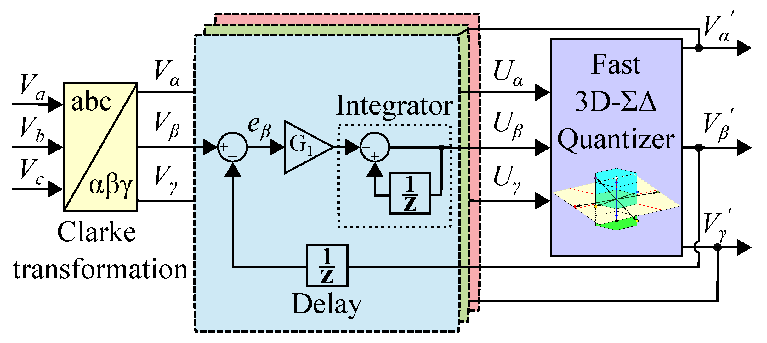
The scheme of the 3D- Σ Δ strategy is illustrated in Figure 2.
To analyse the proposed modulation, it is necessary to define the vector spaces V = ( a , b , c ) t R 3 and W = ( α , β , γ ) t R 3 . Hence, T : V W is then defined as
T = 2 3 1 1 2 1 2 0 3 2 3 2 1 2 1 2 1 2
which is a Clarke transformation.
The 3D- Σ Δ technique works in α β γ reference, so it is necessary to express the reference vector in these coordinates using T. Then, the modulation compares the reference vector to the quantiser outputs ( V α , V β , V γ , ) and integrates the resulting errors ( e α , e β , e γ ). It may be necessary to add gains before the integrations to guarantee the system stability, as is detailed in [33]. Additionally, the modulation may include more integration loops. However, a maximum of two integrators should be used since the modulation may become noisy if three or more integrators are employed [36]. Finally, the integrated errors ( U α , U β , U γ ) are the inputs of the quantiser, whose outputs are compared to the next reference vector.
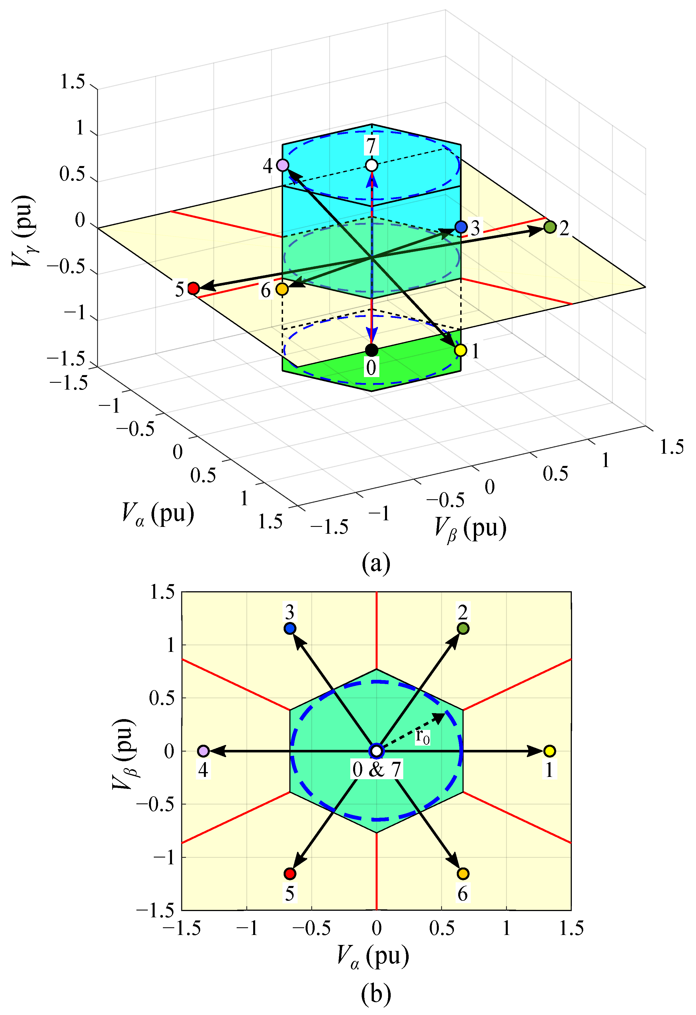
The quantiser divides the vector space W into eight sectors: one for each possible switching vector. Figure 3 shows the sectors of the 3D- Σ Δ modulation. At each sampling instant, the quantiser determines the position and sector of the reference vector and synthesises it by applying the corresponding vector. Note that the switching vector may not be the closest one to the reference vector.
As in H- Σ Δ modulation, the sector can be determined with branch and bound algorithms and by calculating distances from the reference vector to the projection of the possible switching vectors [33]. However, this paper proposes a fast quantiser that simplifies its implementation and reduces the number of required calculations.
The proposed fast quantiser is an improvement on those presented in [34], as the new algorithm allows for working in systems where the homopolar component is not zero. The presented fast quantiser defines the sectors of W as follows:
B 0 = { x W : ( α 2 + β 2 r 0 2 ) ( γ < 0 ) }
B 1 = { x W : ( α 2 + β 2 > r 0 2 ) ( α 0 ) ( k α β < k α ) }
B 2 = { x W : ( α 2 + β 2 > r 0 2 ) ( α 0 ) ( β k α ) }
B 3 = { x W : ( α 2 + β 2 > r 0 2 ) ( α < 0 ) ( β k α ) }
B 4 = { x W : ( α 2 + β 2 > r 0 2 ) ( α < 0 ) ( k α β < k α ) }
B 5 = { x W : ( α 2 + β 2 > r 0 2 ) ( α < 0 ) ( k α > β ) }
B 6 = { x W : ( α 2 + β 2 > r 0 2 ) ( α 0 ) ( k α > β ) }
B 7 = { x W : ( α 2 + β 2 r 0 2 ) ( γ 0 ) }
where k = tan ( π / 6 ) and r 0 = [ 0.67 , 0.77 ] . Note that r 0 can take any value within the specified range, as this does not significantly affect the modulation, as shown in [34].
Given a point in space W, the above expressions can used to determine which sector the point belongs to. The procedure to determine the sector is as follows. First, the boundary values are calculated from the input, i.e., U α 2 + U β 2 and ± k U α . Then, the quantiser compares the input with them and with r 0 . Notice that r 0 has been defined previously. The comparison result is a 5 b word that is used as the address of a read-only memory (ROM). The output of the ROM is the corresponding switching vector, as detailed in Table 2. Figure 4 depicts the flowchart of the proposed fast 3D- Σ Δ modulation. Table 3 quantifies the operations of the proposed fast quantiser and compares them with those of a standard quantizer.

3. Control Strategy

Figure 5 shows the control system used in the active filter. This system allows the compensation of harmonics, reactive power and unbalances in the grid.
First, the algorithm uses a PLL specifically designed to work on distorted and unbalanced grids. This PLL is a rotationary frame sequence detector (RFSD), and its operation is detailed in [37]. The distortion detection algorithm determines the harmonics to be compensated by the filter, the reactive power and the current required to balance the electrical grid. In the filter under study, it is not necessary to determine the harmonics to be compensated, since the current loop incorporates resonant controllers [38]. However, the algorithm does determine the currents required to balance the grid when the load is unbalanced. After determining the required filter currents ( I f ), these are controlled through cascaded resonant controllers within the current loop. These controllers ensure there are no errors in the harmonic frequencies [39,40]. Finally, the current loop outputs are the reference voltages of the 3D- Σ Δ modulation.
In addition to the previous algorithms, the control incorporates a voltage loop to balance the DC-bus and its capacitors. According to [41], the transfer function of the DC-link is
V c ( s ) = 3 v d 2 C d c V c s I d c
where v d is the direct input voltage and V c is the total DC-bus voltage at the operation point. Notice that V c is the sum of the capacitor voltages ( V c = V c h 2 + V c l 2 ). Using (10), a PI controller can be designed to control the DC-bus voltage and balance the capacitors.
The current loop consists of several cascaded PR controllers. Cascaded non-ideal resonant controllers are defined using
G P R ( s ) = k p + h = n h = m 2 k i h ω c s s 2 + 2 ω c s + ( h ω 1 ) 2
where ω 1 is the fundamental frequency, h is the harmonic order to be compensated for, k p is the proportional constant, k i h is the individual resonant gain, and ω c is the bandwidth around the resonant frequency. Notice that the bandwidth can be adjusted by setting ω c appropriately. It may be necessary to tune each resonant controller separately to achieve accurate control.
Resonant controllers can be implemented digitally using second-order IIR filters with the following transfer function:
H ( z ) = b 1 z 1 a 2 z 2 + a 1 z 1 + a 0 .
The filter parameters can be calculated from k i , the resonant frequency ( h ω 1 ), the bandwidth and the sampling time ( T s ). The filter constants are defined as
b 1 = 4 k i T s ω c
a 0 = T s 2 ( h ω 1 ) 2 + 4 T s ω c + 4
a 1 = 2 T s 2 ( h ω 1 ) 2 8
a 2 = T s 2 ( h ω 1 ) 2 4 T s ω c + 4 .

4. Simulation Results

This section evaluates the impact of the proposed 3D- Σ Δ techniques on a VSC with SiC MOSFETs (Figure 1) operating as an APF. To assess the effects of the proposed modulations, the results are compared with those of the SPWM.
An important difference between SPWM and Σ Δ techniques is the switching frequency. The switching frequency is variable in Σ Δ modulations. In these techniques, the maximum switching frequency is always half the sampling frequency. Hence, this work uses the maximum switching frequency ( f m a x ) as a comparison parameter between SPWM and 3D- Σ Δ . The maximum switching frequency is
f m a x = f s for SPWM f s n for 3 D - Σ Δ
where f s is the sampling frequency, and n is an integer such that n 2 n Z ( n = 2 , 3 , 4 , , ) . The modulation index m is within the range of [0, 1].

4.1. System Model

The studied VSC is modeled using MATLAB/Simulink and PLECS Blockset. The rated power of the converter is 25 kVA; the DC-bus voltage is 400 V; and the AC-side currents are constant at their rated values (15 A). The maximum switching frequency is 200 kHz. The SiC MOSFET module FS45MR12W1M1_B11 manufactured by Infineon is used to simulate the converter switches. This module features a maximum drain source voltage ( V d s ) of 1.2 kV and a continuous drain current ( I d ) of 25 A at 75 °C. Each transistor has an external gate resistance of only 10 Ω , the deadtime is 100 ns and their junction temperatures are 90 °C. The PLECS software calculates the losses according to the thermal datasheet and the equations provided by the manufacturer [42]. The electrical grid used for the simulation is a European one with a phase-neutral voltage of 230 V and a frequency of 50 Hz.

4.2. Analysis of Simulation Results

The modulation techniques are studied in a grid-connected active power filter. The simulated APF compensates for the currents generated by a diode rectifier and an unbalanced load. In particular, the filter compensates for current unbalances and all harmonics up to 17. The resonant controllers have been designed to ensure a phase margin of more than 60° and a gain margin of more than 10 dB.
The harmonics and THD of the current have been meticulously calculated using the methodology specified by the IEC 61000-3-2 [43] and IEC 61000-4-7 [44] standards. Consequently, this analysis focuses solely on the initial 40 harmonics. The analysis excludes voltage harmonics, since shunt-connected active power filters are specifically designed to address and compensate for current harmonics. For a comprehensive examination of voltage harmonics resulting from Σ Δ modulations, a detailed analysis is provided in [33]. Regarding efficiency, it is determined through
η = 100 · 1 P l o s s P i n ,
where P l o s s represents the converter losses and P i n represents the input power to the converter.
Figure 6 shows the currents produced by the load. These current waveforms are typical of a diode rectifier and are highly non-linear. The load remains constant throughout the simulation, so the whole system is at steady state. Since the load is unbalanced, the magnitude of the harmonics and THD will vary between phases. The figure only shows phase A in the frequency domain, but all other phases are equivalent. Mainly, the load generates 5th and 7th harmonics, but it also produces other harmonics of significant amplitude, such as the 11th and the 13th. Additionally, the studied load is unbalanced, so currents flow through the neutral of the grid.
Figure 7 plots the simulated grid currents when the APF is compensating for harmonics and unbalances. Figure 7a displays the grid currents when the modulation technique is the SPWM. The three grid currents are balanced, so the APF compensates for unbalances properly. The main current harmonics are lower than those produced by the load. However, some additional harmonics appear, such as 3rd, 9th and 15th harmonics, and others are slightly higher than those generated by the load. This behaviour happens because SPWM modulation may generate harmonics at low frequencies when the switching frequency is high, as discussed in [33,45]. Moreover, the figure shows that the efficiency of SPWM modulation is 94.67%. Figure 7b plots the currents when the APF uses the proposed 3D- Σ Δ strategy. This modulation also balances the currents, but, in addition, it fully compensates all harmonics up to the 17th. This technique does not produce additional harmonics, such as those at low frequencies. However, the ripple of the currents is slightly higher than that produced by an SPWM, since Σ Δ modulations distribute the switching harmonics at medium frequencies [34]. The efficiency of 3D- Σ Δ modulation is 96.40%, which is higher than that of SPWM modulation. This is because Σ Δ modulations operate with a variable switching frequency, enabling them to switch at high frequencies with less loss than modulations that use fixed switching frequencies.

5. Experimental Results

To experimentally validate the 3D- Σ Δ modulation, we used a prototype that incorporates SiC semiconductors (FS45MR12W1M1_B11 from Infineon) from Infineon that were previously simulated. This prototype is designed to withstand powers up to 25 kVA. The SiC module features a maximum drain-source voltage of 1.2 kV and a continuous drain current of 25 A at 75 °C. On the DC side, there was a constant 400 Vdc source. On the AC side, there was a load. The modulation techniques were implemented on a dSPACE DS1006 platform and a DS5203 FPGA board. The 3D- Σ Δ modulation uses the fast quantiser proposed in Section 2 and the control detailed in Section 3. Grid currents were measured with a high-resolution oscilloscope (Agilent InfiniiVision MSO7104A: 1 GHz bandwidth and 4 GS/s sample rate) and current probes (Keysight N2783B: 100 MHz bandwidth). The THD measurement considers only the first 40 harmonics, as detailed in the standards IEC 61000-3-2 [43] and IEC 61000-4-7 [44]. The converter efficiency was measured using a digital power meter (Yokogawa WT1600: 1 MHz bandwidth).
The first experiment aims to compare the efficiency of the proposed 3D- Σ Δ modulation with the SPWM technique. To this end, a three-phase RL load with R = 45.3 Ω and L = 470 μH was connected to the AC side of the converter in an open loop. Moreover, the maximum switching frequency of the converter was 200 kHz. The open loop control was used to adjust the modulation index and examine the converter’s efficiency at different operating points.
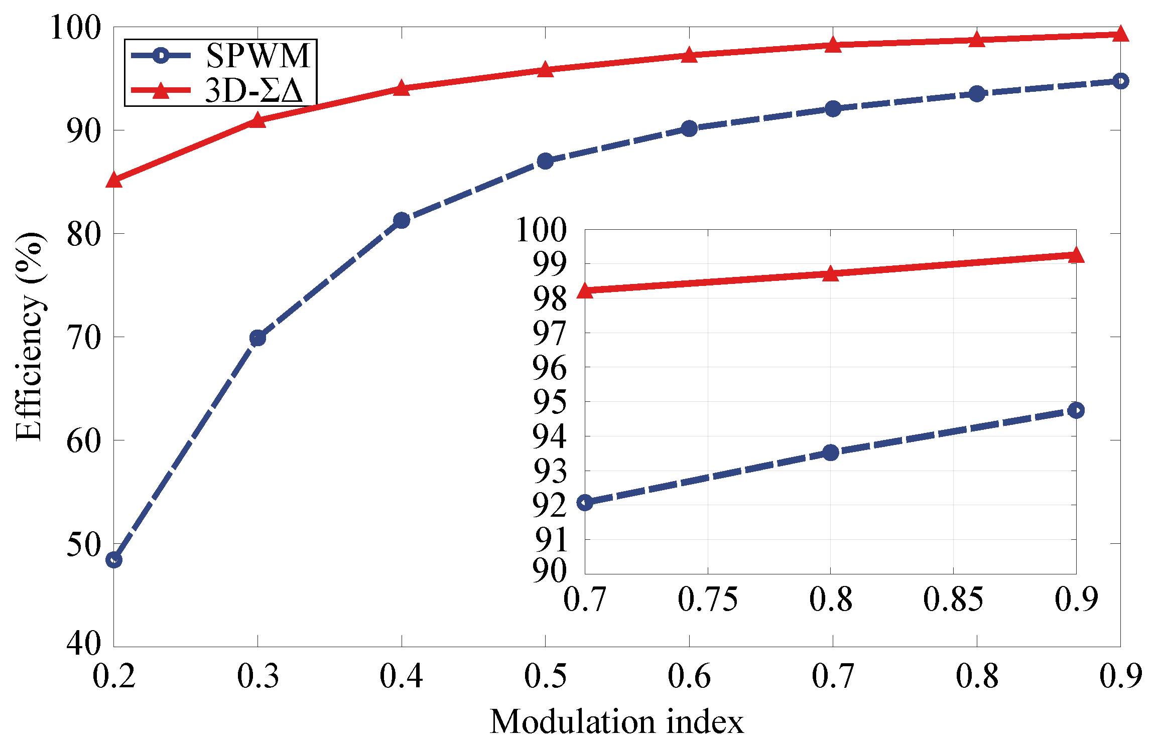
Figure 8 shows the experimental efficiencies of the converter. The results demonstrate that the efficiencies obtained using the 3D- Σ Δ modulation are higher than those obtained using the SPWM technique at all operating points. However, as the modulation index increases, the difference between the two techniques decreases. At m = 0.9, SPWM exhibits slightly lower efficiency than 95%, while 3D- Σ Δ achieves an efficiency close to 99%. This efficiency behaviour is consistent with previous work on Σ Δ modulations [33].
The second experiment employs the converter working as an APF using both the SPWM modulation and the proposed 3D- Σ Δ technique at f m a x = 200 kHz. Figure 9 shows the experimental setup. In this experiment, two loads are connected on the AC side: a non-linear load consisting of a diode rectifier and resistors with R = 40.5 Ω and an unbalanced resistive load with R = 57.6 Ω in phase A and R = 100 Ω in phases B and C.
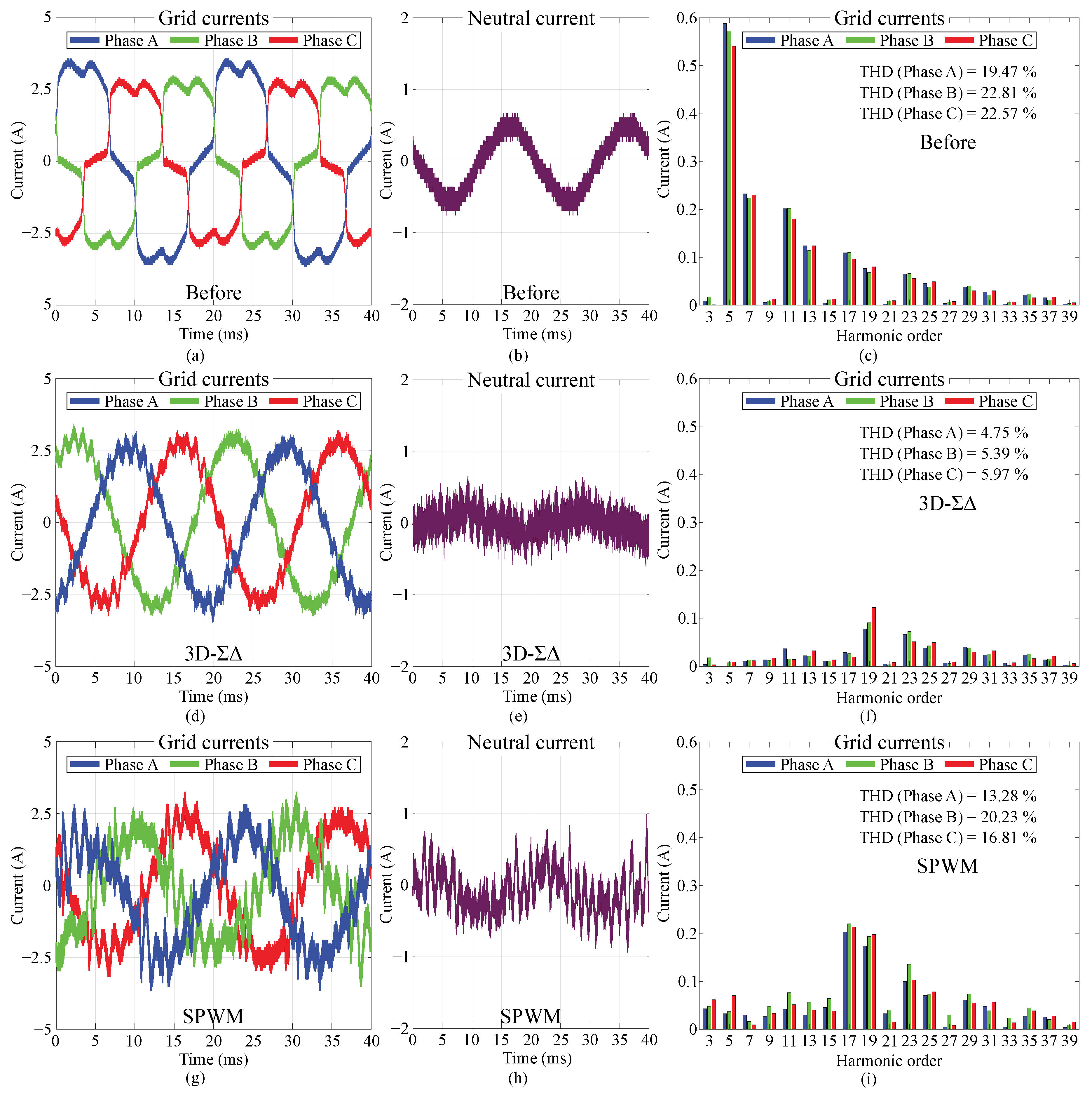
Figure 10 illustrates the results obtained with the converter operating as an APF, i.e., in a closed loop. Figure 10a–c display the results without connecting the filter, i.e., the currents and distortion produced by the load. Figure 10a shows the currents produced by the load. These currents have the typical shape produced by a diode rectifier, and it can be observed that phase A is higher than the others since it has a less resistive load. Figure 10b shows the current in the neutral wire of the grid. This current is produced due to the unbalanced load and is a 50 Hz sine waveform. Figure 10c shows the THD and harmonic distribution of the currents produced by the load. The diode rectifier mainly produces odd harmonics of positive and negative sequences. The most prominent harmonics are the 5th and 7th, but others such as the 11th, 13th, and 17th are also significant. All THDs are similar, but phase A exhibits slightly less THD than the others. Figure 10d–f depict the experimental grid currents when the APF compensates for current harmonics and imbalances using the proposed 3D- Σ Δ . In this experiment, the active filter was compensating for all odd harmonics up to the 17th. Figure 10d illustrates the current supplied by the electrical grid. These currents are sinusoidal and balanced, although they present some harmonic distortion. However, the fact that the grid currents maintain a sinusoidal form indicates that the filter is compensating for harmonics correctly. Additionally, the balanced currents indicate that the APF compensates for the homopolar current that circulates through the neutral. Figure 10e shows the waveform of the neutral current of the electrical grid. The amplitude of this current is low, although it exhibits some ripple. The low value of this current is due to the APF compensating for imbalances. Therefore, there is virtually no homopolar component in the grid. Finally, Figure 10f illustrates the harmonic distortion or THD in the electrical grid currents. The APF compensates for all harmonics up to the 17th, resulting in a significant decrease in the THD to about 5% from around 21%. Figure 10g–i illustrate the results using an SPWM. In this case, the compensation is limited to the 15th harmonic, since a resonance frequency occurs in the 17th harmonic due to the different harmonic spectrum of this modulation. Figure 10g depicts the grid currents. The currents are sinusoidal and nearly balanced, but they have more ripple and imbalance than those achieved using the 3D- Σ Δ modulation. Figure 10h displays the neutral current. The magnitude of this current is low as the filter compensates for the imbalances. However, it shows some ripple. Lastly, Figure 10i presents the grid currents in the frequency domain. The harmonic content and the THD of these currents are higher using the SPWM modulation than the 3D- Σ Δ modulation, as was also observed in the simulation. The increased harmonic content at low frequency is responsible for the ripple seen in the time domain. The THD is slightly reduced in all phases, but the reduction is not as remarkable as that achieved using the 3D- Σ Δ modulation.
In summary, the experimental results presented in Figure 10d–f demonstrate the effectiveness of the APF in compensating for current harmonics and imbalances in the electrical grid using the proposed 3D- Σ Δ modulation. Moreover, this modulation enables a higher THD reduction and a higher performance than using the SPWM technique.

6. Conclusions

This article proposes a novel 3D- Σ Δ modulation technique for three-leg four-wire voltage source converters based on wide-bandgap semiconductors. This technique enables a variable switching frequency, which significantly reduces losses compared to fixed switching frequency modulations. Moreover, the proposed technique allows compensating for homopolar currents in four-wire systems. Additionally, a fast quantiser is proposed to simplify the implementation of the proposed modulation and reduce its computational cost. Experimental results demonstrate the effectiveness of the proposed technique. The performance of the 3D- Σ Δ modulation is compared with the SPWM technique at different operating points. The results show that the 3D- Σ Δ modulation produces much lower losses at high switching frequencies than the classical SPWM modulation. Moreover, the proposed modulation is implemented in a power converter operating as an active power filter and compared with an SPWM technique. The experimental results demonstrate that the 3D- Σ Δ technique effectively compensates for positive and negative sequence harmonics as well as zero sequence currents. Furthermore, it is able to reduce the harmonic distortion in the electrical grid more than the SPWM modulation can, making it a better solution for maintaining a high power quality. In summary, the proposed 3D- Σ Δ technique is suitable for application to three-leg three-wire and four-wire active power filters and can compensate for harmonics and unbalances in the electrical grid more effectively than other fixed-frequency modulations with fewer losses.

Author Contributions

D.L. assumed primary responsibility for drafting the paper, simulating the studied modulations, and conducting the presented experiments. M.L. and N.B. implemented the control loop. J.Z. and E.R.-C. thoroughly revised and corrected the initial manuscript. All authors conducted the final review. All authors have read and agreed to the published version of the manuscript.

Funding

This work was supported by the Industrial Doctorates Plan of the Secretaria d’Universitats i Recerca del Departament d’Empresa i Coneixement de la Generalitat de Catalunya, and the Ministerio de Ciencia e Innovación of Spain within the projects PID2019-111420RB-I00 and PID2022-138827OB-I00.

Data Availability Statement

Data are contained within the article.

Conflicts of Interest

The authors declare no conflict of interest.

References

  1. Kazmierkowski, M.P. Power quality: Problems and mitigation techniques [book news]. IEEE Ind. Electron. Mag. 2015, 9, 62. Available online: http://ieeexplore.ieee.org/document/7128811/ (accessed on 15 August 2023). [CrossRef]
  2. Li, H.; Li, B.; Luo, Z.; Li, H.; Zhao, Y.; Wang, T.; Sun, Y. Power Supply Reliability Enhancement for Low-Voltage Distribution Area with Power Quality Improvement Function. IEEE Access 2022, 10, 130619–130631. [Google Scholar] [CrossRef]
  3. Garcia, C.A.I.; Bindi, M.; Corti, F.; Luchetta, A.; Grasso, F.; Paolucci, L.; Piccirilli, M.C.; Aizenberg, I. Power Quality Analysis Based on Machine Learning Methods for Low-Voltage Electrical Distribution Lines. Energies 2023, 16, 3627. [Google Scholar] [CrossRef]
  4. Santiago, I.; López-Rodríguez, M.A.; de Castro, A.G.; Moreno-Munoz, A.; Luna-Rodríguez, J.J. Energy consumption of audiovisual devices in the residential sector: Economic impact of harmonic losses. Energy 2013, 60, 292–301. [Google Scholar] [CrossRef]
  5. Franquelo, L.G.; Prats, M.Á.M.; Portillo, R.C.; Galvan, J.I.L.; Perales, M.A.; Carrasco, J.M.; Díez, E.G.; Jiménez, J.L.M. Three-dimensional space-vector modulation algorithm for four-leg multilevel converters using abc coordinates. IEEE Trans. Ind. 2006, 53, 458–466. [Google Scholar] [CrossRef]
  6. Fabricio, E.L.L.; Silva, S.C.; Jacobina, C.B.; Corrêa, M.B.D.R. Analysis of main topologies of shunt active power filters applied to four-wire systems. IEEE Trans. Power Electron. 2018, 33, 2100–2112. [Google Scholar] [CrossRef]
  7. Luo, F.; Loo, K.H.; Lai, Y.M. Simple carrier-based pulse-width modulation scheme for three-phase four-wire neutral-point-clamped inverters with neutral-point balancing. IET Power Electron. 2016, 9, 365–376. [Google Scholar] [CrossRef]
  8. Lumbreras, D.; Gálvez, E.; Collado, A.; Zaragoza, J. Trends in power quality, harmonic mitigation and standards for light and heavy industries: A review. Energies 2020, 13, 5792. Available online: https://www.mdpi.com/1996-1073/13/21/5792 (accessed on 22 October 2023). [CrossRef]
  9. Siemens. SINAMICS G130/G150 Line Harmonics Filter. Operating Instructions 07/2007 Edition. 2007. Available online: https://cache.industry.siemens.com/dl/files/997/26576997/att_73840/v1/SINAMICS_G130_G150_LHF_0707_eng.pdf (accessed on 22 October 2023).
  10. ABB. Power Quality Filters—PQFI—PQFM—PQFS. Electrification Products. 2017. Available online: https://search.abb.com/library/Download.aspx?DocumentID=9AKK106930A8906&LanguageCode=en&DocumentPartId=&Action=Launch (accessed on 5 June 2023).
  11. Circutor. AFQm Multifunction Active Filter. 2022. Available online: https://circutor.com/pdf/pdfdatasheet.php?lang=es&prod=R7MM2F (accessed on 17 September 2023).
  12. Popescu, M.; Bitoleanu, A.; Linca, M.; Suru, C.V. Improving power quality by a four-wire shunt active power filter: A case study. Energies 2021, 14, 1951. [Google Scholar] [CrossRef]
  13. Kim, J.-H.; Sul, S.-K. A carrier-based pwm method for three-phase four-leg voltage source converters. IEEE Trans. Power Electron. 2004, 19, 66–75. Available online: http://ieeexplore.ieee.org/document/1262054/ (accessed on 9 November 2023). [CrossRef]
  14. Perales, M.A.; Prats, M.M.; Portillo, R.; Mora, J.L.; León, J.I.; Franquelo, L.G. Three-dimensional space vector modulation in abc coordinates for four-leg voltage source converters. IEEE Power Electron. Lett. 2003, 1, 104–109. [Google Scholar] [CrossRef]
  15. Viatkin, A.; Mandrioli, R.; Hammami, M.; Ricco, M.; Grandi, G. Ac current ripple harmonic pollution in three-phase four-leg active front-end ac/dc converter for on-board EV chargers. Electronics 2021, 10, 116. [Google Scholar] [CrossRef]
  16. Pires, V.F.; Cordeiro, A.; Foito, D.; Pires, A.J.; Hao, C.; Martins, J.F.; Castro, R. Compensation of Unbalanced Low-Voltage Grids Using a Photovoltaic Generation System with a Dual Four-Leg, Two-Level Inverter. Electronics 2022, 11, 320. [Google Scholar] [CrossRef]
  17. Prats, M.; Franquelo, L.; Portillo, R.; León, J.; Galván, E.; Carrasco, J. A 3-d space vector modulation generalized algorithm for multilevel converters. IEEE Power Electron. Lett. 2003, 1, 110–114. [Google Scholar] [CrossRef]
  18. Dai, N.-Y.; Wong, M.-C.; Ng, F.; Han, Y.-D. A fpga-based generalized pulse width modulator for three-leg center-split and four-leg voltage source inverters. IEEE Trans. Power Electron. 2008, 23, 1472–1484. Available online: http://ieeexplore.ieee.org/document/4494750/ (accessed on 17 September 2023). [CrossRef]
  19. Mandrioli, R.; Viatkin, A.; Hammami, M.; Ricco, M.; Grandi, G. Variable switching frequency pwm for three-phase four-wire split-capacitor inverter performance enhancement. IEEE Trans. Power Electron. 2021, 36, 13674–13685. [Google Scholar] [CrossRef]
  20. Mandrioli, R.; Viatkin, A.; Hammami, M.; Ricco, M.; Grandi, G. A comprehensive ac current ripple analysis and performance enhancement via discontinuous pwm in three-phase four-leg grid-connected inverters. Energies 2020, 13, 4352. Available online: https://www.mdpi.com/1996-1073/13/17/4352 (accessed on 5 June 2023). [CrossRef]
  21. Li, B.; Li, Q.; Lee, F.C.; Liu, Z.; Yang, Y. A high-efficiency high-density wide-bandgap device-based bidirectional on-board charger. IEEE J. Emerg. Sel. Top. Power Electron. 2018, 6, 1627–1636. [Google Scholar] [CrossRef]
  22. Zhang, Z.; Zhu, Z.; Hu, B.; Tang, X.; Liu, C.; Wang, Z. Uniform carrier-based pwm method for three-phase three-level three-wire and four-wire converter system with neutral-point balancing. IET Power Electron. 2020, 13, 3081–3089. [Google Scholar] [CrossRef]
  23. Wang, W.; Zhang, B.; Xie, F. A novel svpwm for three-level npc inverter based on m-mode controllability. IEEE Trans. Ind. 2018, 65, 6055–6065. Available online: http://ieeexplore.ieee.org/document/8240695/ (accessed on 12 July 2023). [CrossRef]
  24. Chen, H.-C.; Tsai, M.-J.; Wang, Y.-B.; Cheng, P.-T. A modulation technique for neutral point voltage control of the three-level neutral-point-clamped converter. IEEE Trans. Ind. Appl. 2018, 54, 2517–2524. Available online: https://ieeexplore.ieee.org/document/8274978/ (accessed on 20 November 2023). [CrossRef]
  25. Millan, J.; Godignon, P.; Perpina, X.; Perez-Tomas, A.; Rebollo, J. A survey of wide bandgap power semiconductor devices. IEEE Trans. Power Electron. 2014, 29, 2155–2163. Available online: http://ieeexplore.ieee.org/document/6532359/ (accessed on 20 November 2023). [CrossRef]
  26. Shenai, K. High-density power conversion and wide-bandgap semiconductor power electronics switching devices. Proc. IEEE 2019, 107, 2308–2326. [Google Scholar] [CrossRef]
  27. Gonzalez, J.O.; Wu, R.; Jahdi, S.; Alatise, O. Performance and reliability review of 650 v and 900 v silicon and sic devices: Mosfets, cascode jfets and igbts. IEEE Trans. Ind. Electron. 2020, 67, 7375–7385. [Google Scholar] [CrossRef]
  28. Lumbreras, D.; Zaragoza, J.; Mon, J.; Gálvez, E.; Collado, A. Efficiency analysis of wide band-gap semiconductors for two-level and three-level power converters. In Proceedings of the IECON 2019—45th Annual Conference of the IEEE Industrial Electronics Society, Lisbon, Portugal, 14–17 October 2019; pp. 5126–5133. Available online: https://ieeexplore.ieee.org/document/8926766/ (accessed on 8 June 2023). [CrossRef]
  29. Xue, F.; Yu, R.; Huang, A.Q. A 98.3% efficient gan isolated bidirectional dc-dc converter for dc microgrid energy storage system applications. IEEE Trans. Ind. Electron. 2017, 64, 9094–9103. Available online: http://ieeexplore.ieee.org/document/7885035/ (accessed on 14 October 2023). [CrossRef]
  30. Li, H.; Zhang, Z.; Wang, S.; Tang, J.; Ren, X.; Chen, Q. A 300-khz 6.6-kw sic bidirectional llc onboard charger. IEEE Trans. Ind. Electron. 2020, 67, 1435–1445. [Google Scholar] [CrossRef]
  31. Matallana, A.; Ibarra, E.; López, I.; Andreu, J.; Garate, J.I.; Jordà, X.; Rebollo, J. Power module electronics in hev/ev applications: New trends in wide-bandgap semiconductor technologies and design aspects. Renew. Sustain. Energy Rev. 2019, 113, 109264. [Google Scholar] [CrossRef]
  32. Lumbreras, D. Development of an Active Power Filter Based on Wide-Bandgap Semiconductors. 2022. Available online: http://hdl.handle.net/10803/675092 (accessed on 8 June 2023).
  33. Lumbreras, D.; Zaragoza, J.; Berbel, N.; Mon, J.; Galvez, E.; Collado, A. Comprehensive analysis of hexagonal sigma-delta modulations for three-phase high-frequency vsc based on wide-bandgap semiconductors. IEEE Trans. Power Electron. 2021, 36, 7212–7222. Available online: https://ieeexplore.ieee.org/document/9266054/ (accessed on 28 November 2023). [CrossRef]
  34. Lumbreras, D.; Zaragoza, J.; Berbel, N.; Mon, J.; Galvez, E.; Collado, A. Fast-processing sigma–delta strategies for three-phase wide-bandgap power converters with common-mode voltage reduction. IEEE Trans. Power Electron. 2022, 37, 7989–8000. Available online: https://ieeexplore.ieee.org/document/9699032/ (accessed on 28 November 2023). [CrossRef]
  35. Acosta-Cambranis, F.; Zaragoza, J.; Martinez, L.R.; Berbel, N. New modulation strategy for five-phase high-frequency vsi based on sigma-delta modulators. IEEE Trans. Power Electron. 2021, 14, 3943–3953. Available online: https://ieeexplore.ieee.org/document/9582737/ (accessed on 28 November 2023). [CrossRef]
  36. Candy, J. A use of double integration in sigma delta modulation. IEEE Trans. Commun. 1985, 33, 249–258. Available online: http://ieeexplore.ieee.org/document/1096276/ (accessed on 14 October 2023). [CrossRef]
  37. Robles, E.; Ceballos, S.; Pou, J.; Martín, J.L.; Zaragoza, J.; Ibañez, P. Variable-frequency grid-sequence detector based on a quasi-ideal low-pass filter stage and a phase-locked loop. IEEE Trans. Power Electron. 2010, 25, 2552–2563. Available online: http://ieeexplore.ieee.org/document/5466221/ (accessed on 28 November 2023). [CrossRef]
  38. Asiminoael, L.; Blaabjerg, F.; Hansen, S. Detection is key - harmonic detection methods for active power filter applications. IEEE Ind. Appl. Mag. 2007, 13, 22–33. Available online: https://ieeexplore.ieee.org/document/4283506/ (accessed on 14 October 2023). [CrossRef]
  39. Liserre, M.; Teodorescu, R.; Blaabjerg, F. Multiple harmonics control for three-phase grid converter systems with the use of pi-res current controller in a rotating frame. IEEE Trans. Power Electron. 2006, 21, 836–841. Available online: http://ieeexplore.ieee.org/document/1629027/ (accessed on 28 November 2023). [CrossRef]
  40. Teodorescu, R.; Blaabjerg, F.; Liserre, M.; Loh, P. Proportional-resonant controllers and filters for grid-connected voltage-source converters. IEE Proc.-Electr. Power Appl. 2006, 153, 750. Available online: http://digital-library.theiet.org/content/journals/10.1049/ip-epa_20030009 (accessed on 28 November 2023). [CrossRef]
  41. Campanhol, L.B.G.; da Silva, S.A.O.; Goedtel, A. Application of shunt active power filter for harmonic reduction and reactive power compensation in three phase four-wire systems. IET Power Electron. 2014, 7, 2825–2836. [Google Scholar] [CrossRef]
  42. PLECS User Manual, 4th ed.; Plexim GmbH: Zurich, Switzerland, 2019.
  43. EN 61000-3-2:2019; Electromagnetic Compatibility (EMC). Part 3-2: Limits. Limits for Harmonic Current Emissions (Equipment Input Current =16 A per Phase). (IEC 61000-3-2:2018). CENELEC: Brussels, Belgium, 2019.
  44. EN 61000-4-7:2004; Electromagnetic Compatibility (EMC). Part 4-7: Testing and Measurement Techniques. General Guide on Harmonics and Interharmonics Measurements and Instrumentation, for Power Supply Systems and Equipment Connected Thereto. CENELEC: Brussels, Belgium, 2004.
  45. Holmes, D. A general analytical method for determining the theoretical harmonic components of carrier based pwm strategies. In Proceedings of the 1998 IEEE Industry Applications Conference. Thirty-Third IAS Annual Meeting (Cat. No.98CH36242), St. Louis, MO, USA, 12–15 October 1998; Volume 2, pp. 1207–1214. Available online: http://ieeexplore.ieee.org/document/730300/ (accessed on 28 November 2023). [CrossRef]
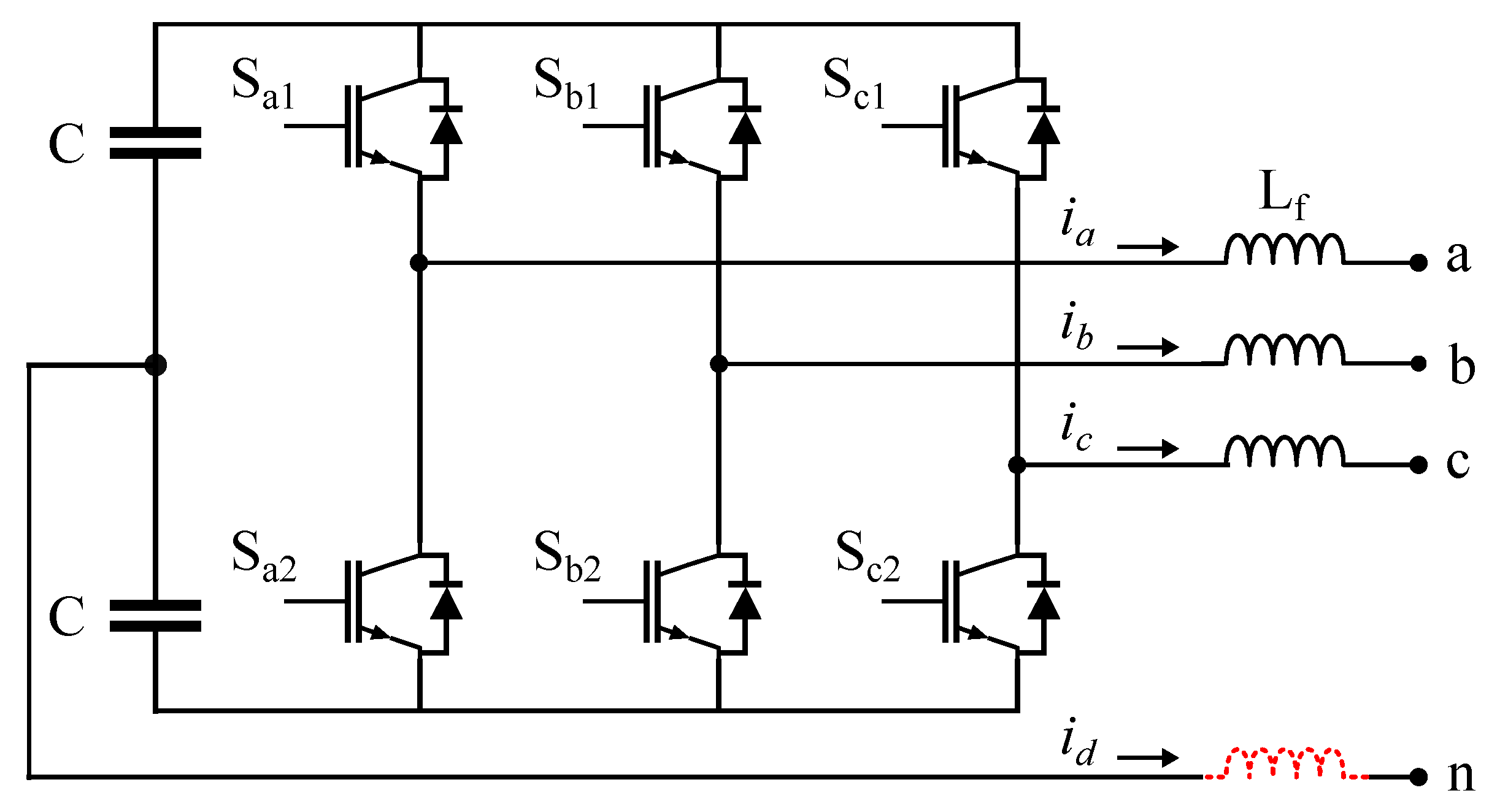
Figure 1. Three-leg four-wire voltage source converter. The red dashed line indicates the option for connecting an optional inductance to the neutral wire.
Electronics 13 00553 g001
Figure 2. Three-dimensional sigma-delta modulation loop. The nominal value of all gains is unity.
Electronics 13 00553 g002
Figure 3. Two-level, three-phase converter switching states: (a) isometric view and (b) view from the zero-sequence axis.
Electronics 13 00553 g003
Figure 4. Flowchart of the proposed 3D- Σ Δ technique.
Electronics 13 00553 g004
Figure 5. Overall block diagram control of the active power filter.
Electronics 13 00553 g005
Figure 6. Characteristics of the simulated load.
Electronics 13 00553 g006
Figure 7. Simulated grid currents when the active power filter is compensating for harmonics and balancing the grid using different modulation strategies: (a) SPWM and (b) 3D- Σ Δ .
Electronics 13 00553 g007
Figure 8. Experimental converter efficiency curves at f m a x = 200 kHz.
Electronics 13 00553 g008
Figure 9. View of the experimental setup: (a) schematic; (b) photographic depiction.
Electronics 13 00553 g009
Figure 10. Experimental results. (ac) Before filtering and balancing. (df) After filtering and balancing using 3D- Σ Δ . (df) After filtering and balancing using SPWM. (a,d,g) Grid current waveforms. (b,e,h) Neutral current waveforms. (c,f,i) Grid currents in frequency domain.
Electronics 13 00553 g010
Table 1. Scope of previous modulation works.
ReferenceYearModulationConverter
Topology
Modulation
Type
Max. Switching
Frequency
[17]20033D SVM3L4WVectorial
[18]20083D PWM3/4L4WPWM5 kHz
[19]2021VSF-PWM3L4WSpread-spectrum5.1 kHz
[20]2020Several PWM3L4WPWM3.6 kHz
[21]2018Simplified PWM3L4WPWM10 kHz
[22]2020CB-PWM3L3/4WPWM20 kHz
[23]201818-mode SVPWM3L4WPWM10 kHz
[24]2018Dipolar PWM3L3/4WPWM10 kHz
This paper20233D- Σ Δ 3L3/4WSpread-spectrum200 kHz
Table 2. Determination of the sector in 3D- Σ Δ .
U α 2 + U β 2 r 0 2 U γ 0 U α 0 U β kU α U β kU α SectorSwitching State
0Indifferent000 B 5 −1−11
0Indifferent001Indifferent
0Indifferent010 B 4 −111
0Indifferent011 B 3 11−1
0Indifferent100 B 6 1−11
0Indifferent101 B 1 1−1−1
0Indifferent110Indifferent
0Indifferent111 B 2 11−1
10IndifferentIndifferentIndifferent B 0 −1−1−1
11IndifferentIndifferentIndifferent B 7 111
Table 3. Operations of the different quantisers for 3D- Σ Δ .
Standard 3D- Σ Δ Fast 3D- Σ Δ
Additions71
Subtractions140
Multiplications144
Comparisons15
ROMNoYes
Total3610
Disclaimer/Publisher’s Note: The statements, opinions and data contained in all publications are solely those of the individual author(s) and contributor(s) and not of MDPI and/or the editor(s). MDPI and/or the editor(s) disclaim responsibility for any injury to people or property resulting from any ideas, methods, instructions or products referred to in the content.