Article

Evaluation of the Electronic Properties of Atomic Layer Deposition-Grown Ge-Doped Zinc Oxide Thin Films at Elevated Temperatures

by
Rafał Knura
1,
Katarzyna Skibińska
1,
Sylvester Sahayaraj
1,
Marianna Marciszko-Wiąckowska
2,
Jakub Gwizdak
3,
Marek Wojnicki
1,3,*,
Piotr Żabiński
3,
Grzegorz Sapeta
1,
Sylwester Iwanek
1 and
Robert P. Socha
1
1
CBRTP SA Research and Development Center of Technology for Industry, Ludwika Waryńskiego 3A, 00-645 Warszawa, Poland
2
Academic Centre for Materials and Nanotechnology, AGH University of Krakow, Al. Mickiewicza 30, 30-059 Kraków, Poland
3
Faculty of Non-Ferrous Metals, AGH University of Krakow, Al. Mickiewicza 30, 30-059 Kraków, Poland
*
Author to whom correspondence should be addressed.
Electronics 2024, 13(3), 554; https://doi.org/10.3390/electronics13030554
Submission received: 19 December 2023 / Revised: 24 January 2024 / Accepted: 26 January 2024 / Published: 30 January 2024

Abstract

:
The aim of this study was to determine the electronic properties of as-deposited ALD-grown Ge-doped zinc oxide thin films annealed at 523 K or 673 K. SEM, EDS, and ellipsometry measurements confirmed that the Ge-doped zinc oxide films with a thickness of around 100 nm and uniform composition were successfully obtained. GI-XRD measurements did not reveal phases other than the expected Wurtzite structure of the ZnO. The electronic properties, i.e., conductivity, charge carrier concentration, and mobility of the films, were evaluated using Hall effect measurements and explained based on corresponding XPS measurements. This work supports the theory that oxygen vacancies act as electron donors and contribute to the intrinsic n-type conductivity of ZnO. Also, it is shown that the effect of oxygen vacancies on the electronic properties of the material is stronger than the effect introduced by Ge doping.

1. Introduction

Zinc oxide (ZnO) is a versatile semiconductor material with a wide bandgap, which endows it with substantial optical and electrical properties. It is well-known for its high electron mobility, strong thermal conductivity, and stability under harsh conditions, making it a suitable candidate for a range of applications, from electronics to environmental technology. The unique properties of ZnO can be further enhanced by doping with metallic elements such as gold (Au) [1] and copper (Cu) [2], or other oxides like Ge(IV) [3], Mn(II) [4], etc.
At the nano and quantum scales, these materials exhibit quantum confinement effects, which influence their electronic and optical behaviors. The quantum effects can lead to tuning of the bandgap and size-dependent optical properties. The combination of ZnO’s intrinsic semiconductor properties with the unique characteristics imparted by Ge doping at the nano and quantum levels opens up exciting opportunities in various high-tech applications, including renewable energy, environmental remediation, and advanced electronics.
Atomic layer deposition (ALD) is a powerful technique for depositing thin films in a thickness range from a few atomic layers to several hundreds of nanometers. Some of the distinct advantages of ALD include precise control of the film thickness, uniform deposition of pinhole-free films over large areas, and its ability to deposit conformally on surfaces [5]. ALD finds extensive application in the field of silicon microelectronics, which requires precise control and conformality [6]. Additionally, it allows the synthesis of metal sulfides [7,8] for energy and photonic applications [9,10].
Above all, ALD is also used to grow thin films of metal oxides (MO) [11], e.g., ZnO [12,13,14,15,16], Al2O3 [17,18], and TiO2 [19,20]. Zinc oxide is a transparent oxide semiconductor with a direct band gap Eg = 3.4 eV [21]. It crystallizes in a hexagonal system called Wurtzite [22]. Due to its simplicity in synthesis by various methods [23], the attractiveness of this compound increases. ZnO, grown by ALD, can be applied, for example, in thin-film transistors [24,25], light-emitting diodes [26,27], and coatings for Li-ion battery electrodes [28].
Naturally, ZnO shows n-type conductivity. Due to this fact, it is difficult to produce p-type conductivity in this compound [12]. For n-doping of ZnO, elements from groups IIIB [29,30], IVA, and IVB [31,32] are usually used. In the case of group IV, the simple hydrogen-like substitutional donor model cannot be applied anymore as dopants are forming defect complexes acting like shallow donors [33].
Several studies have previously addressed the investigation of defects and electron properties in Ge-doped zinc oxide (Ge:ZnO) [34,35]. Nevertheless, there is a noticeable scarcity of research specifically delving into the electronic properties of thin films at elevated temperatures. This gap in the literature is particularly noteworthy given the myriad potential applications that necessitate operation under elevated temperatures, including but not limited to the realm of thermoelectric devices [36,37]. The unique challenges and opportunities posed by elevated temperature conditions make it imperative to delve deeper into the electronic behaviors of thin Ge:ZnO films in such environments. Consequently, a comprehensive exploration of the electronic properties under elevated temperatures is essential for advancing our understanding and unlocking the full potential of Ge:ZnO thin films in various technological applications.
Most frequently, the Ge/ZnO multilayer films have been prepared by rf magnetron sputtering [3]. The materials obtained in this way usually have a large thickness compared to the ALD method. Physical, optical, and electrical properties may also vary due to the uneven distribution of doping components. Ge/ZnO materials can also be obtained by the solid-state reaction method [38]. Unfortunately, the control of the process is limited only to time, temperature, and the degree of grinding of the reacting ingredients. As a result, control of optical and electrical properties is practically impossible.
In this work, Ge:ZnO thin films were deposited using ALD. To date, there has been a single publication detailing the synthesis of Ge:ZnO using ALD [34]. However, in this paper, thin films were fabricated in the large-scale ALD reactor at mild temperature conditions. The large-scale ALD instrument offers the possibility of mass-scale production of thin films, especially ZnO, as it is relatively easy to deposit. The drawbacks of this instrument include long process times at elevated temperature and low pressure, which can have an impact on the thermal budget of the process, and an increased cost of one process due to larger power and precursor consumption for small batches. Furthermore, samples were annealed in a constant flow of dry air at 523 K or 673 K for 4 h. The temperature values of 523 K and 673 K were chosen based on the literature review of annealing ZnO thin films [35,39] and nanomaterials [40], so that effects related to activation of defect migration, such as VZn at ~540 K [41], could be observed and interpreted. Fabrication of films using the industrial system highlights their possible application in electronics or optoelectronics.

2. Materials and Methods

2.1. Fabrication of the Thin Films

2.1.1. Atomic Layer Deposition

Ge-doped ZnO thin films were synthesized using the atomic layer deposition method following the procedure described by Chalker et al. [34], adjusted to the conditions of the large-scale reaction chamber. The deposition was performed in a Beneq P400A ALD system at 473 K and 1 hPa of carrier gas pressure in the reaction chamber. Diethylzinc (DEZ) (Lanxess Organometallics GmbH, Berkgamen, Germany) and tetramethoxygermanium (GEME) (Gelest, Inc. Morrisville, NC, USA) were used as sources of Zn and Ge, respectively, with water vapor as a co-reactant. The precursors were kept at room temperature and introduced to the reaction chamber via vapor draw. Every pulse of metal precursor was followed by two pulses of water to ensure a high degree of reaction. The pulse times of DEZ and GEME lasted 0.3 s, while the water pulse lasted 0.5 s. After each step, the chamber was purged with N2 with 99.999% purity (PSA Nitrogen Gas Generator, Parker, Dukesway Gateshead, UK) for 2 s. The Ge doping was realized by uniformly spacing GeOx layers between stacks of ZnOx layers, so that the desired stoichiometry could be achieved. The achieved growth per cycle was 0.16 nm/cycle for undoped ZnO and decreased to 0.14 nm/cycle for 20% Ge:ZnO.
Two different substrates were used for the film growth: 1 mm thick quartz glass (Helma, Müllheim, Germany) and 0.18 mm thick ultra-flat single-side polished silicon wafers Si <100> (Alpha Nanotech Inc, Vancouver, Canada). Before the deposition, quartz substrates were additionally cleaned. Firstly, in 2% Hellmanex III solution (Helma Analytics, Müllheim, Germany) in an ultrasonic cleaner at 353 K for 5 min, followed by rinsing using deionized water. Then, submerged in isopropanol in an ultrasonic cleaner at 323 K for 5 min, followed again by rinsing in deionized water. Cleaned samples were stored in deionized water and dried with nitrogen before use.
Additionally, just before deposition the surface of both types of substrates were treated by argon plasma using plasma cleaner Diener Tetra 30. Process pressure was 0.3 mbar, and the applied power was equal to 120 W during 2 min.

2.1.2. Annealing of the Films

Samples deposited on the quartz substrates were annealed in a tube furnace in a constant flow of dry air of approximately 100 mL/min at 523 K or 673 K for 4 h at on overpressure of 3 kPa relative to ambient conditions. The heating rate was 5 K/min. Next, the samples were cooled down with the furnace.

2.2. Film Characterization

2.2.1. Scanning Electron Microscopy (SEM)

The ratio of Ge/(Ge + Zn), i.e., the amount of substituting germanium, was determined using a JEOL JCM-6000 scanning electron microscope (Freising, Germany) equipped with an energy-dispersive X-ray spectroscopy (EDS) detector.

2.2.2. X-ray Diffraction

The X-ray diffraction was carried out using a PANalytical Empyrean diffractometer (by Malvern Panalytical Co., Almelo, the Netherlands, and Malvern, UK) with Cu Kα radiation and a parallel beam geometry (Göbel mirror in the incident beam optics and parallel plate collimator in the diffracted beam optics) over the 2θ range of 25–45°, step 0.02°, at room temperature. Diffraction patterns were collected using the grazing-incidence X-ray diffraction method (GIXRD) with an incident angle of 1°.

2.2.3. Laser Ellipsometry

The thickness of the films was confirmed using a Sentech SE400adv ellipsometer (Berlin, Germany) at an incident angle of 70°.

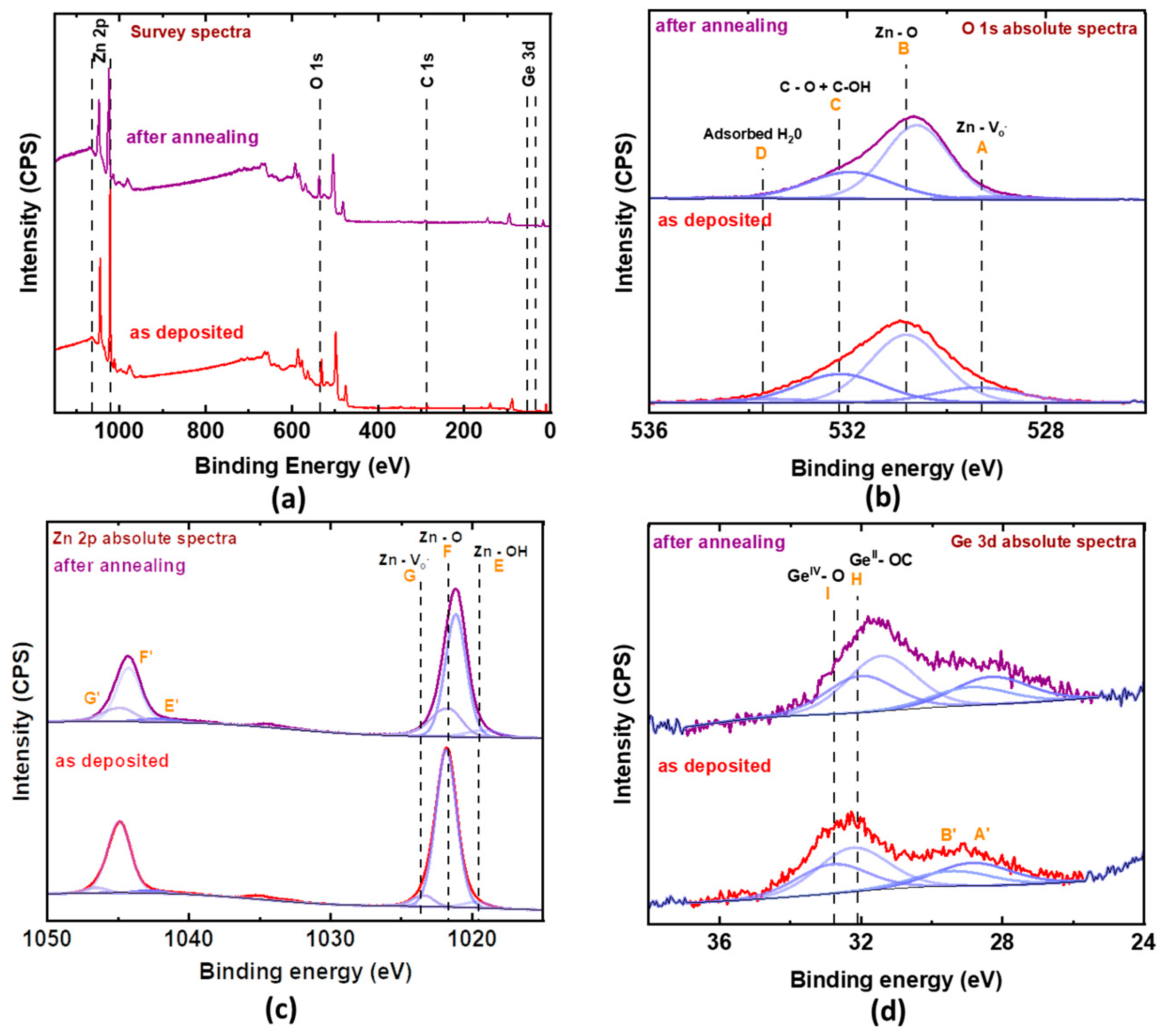
2.2.4. X-ray Photoelectron Spectroscopy (XPS)

The X-ray photoelectron spectra (XPS) were recorded using an EA 15 (PREVAC) hemispherical analyzer (Rogów, Poland) equipped with a dual-anode X-ray source, RS 40B1 (PREVAC). The measurements were performed using Al Kα (1486.6 eV) radiation and an analyzer pass energy of 100 eV. The spectra were recorded in normal emission geometry with an energy resolution of 0.9 eV. The spectrometer was calibrated with the Ag, Au, and Cu foil according to ISO standard 15472:2010 [42]. Ultra-high vacuum (UHV) conditions of 8 × 10⁻⁹ mbar were maintained during the measurements. The area of analysis was approximately 3 mm2, and the depth of analysis was about 10 nm. The samples were mounted and positioned in the dedicated holder, pumped out to high vacuum, and then transferred into the UHV chamber. The survey and high-resolution spectra were acquired. The spectra were analyzed with the use of CasaXPS (version 2.3.24PR) software. The electron binding energy (BE) scale was calibrated for the Fermi edge at 0.0 eV. A Shirley-type spectrum background was used. The highly resolved spectra were deconvoluted with the Voigt function (Gauss-to-Lorentz profile ratio of 70:30). The spectra were compared, respectively, to the background level.

2.2.5. Electrical Properties

The electronic properties of samples were measured using the ECOPIA Hall effect measurement system (HMS-5500, Warsaw, Poland) from room temperature up to 523 K in N2 flow (99.999%). The measurement was performed using van der Pauw geometry with contact needles attached to the corners of a square sample. The sample has been contacted by gold-coated needles carefully placed at the corners of the sample while ensuring that the current–voltage plots between two consecutive needles produce an ohmic resistance (straight line) of similar values (slope). The estimated contact point area was smaller than 0.25 mm2.
Depending on the characterization method, two different substrates were used—quartz glass for XRD and Hall effect measurements and Si wafer for SEM/EDS and Ellipsometry methods.

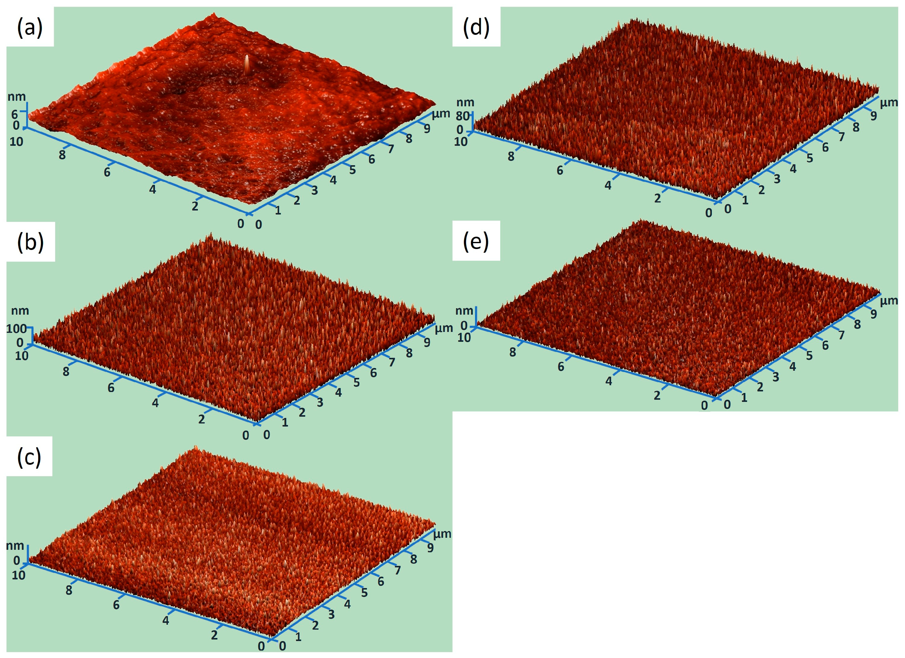
2.2.6. Atomic force microscopy (AFM) Analysis

AFM measurements were performed using an NTegra Aura NT MDT setup (Moscow, Russia) in semicontact mode using an NSG03 tip to obtain the 3D topography images of the films.

3. Results and Discussion

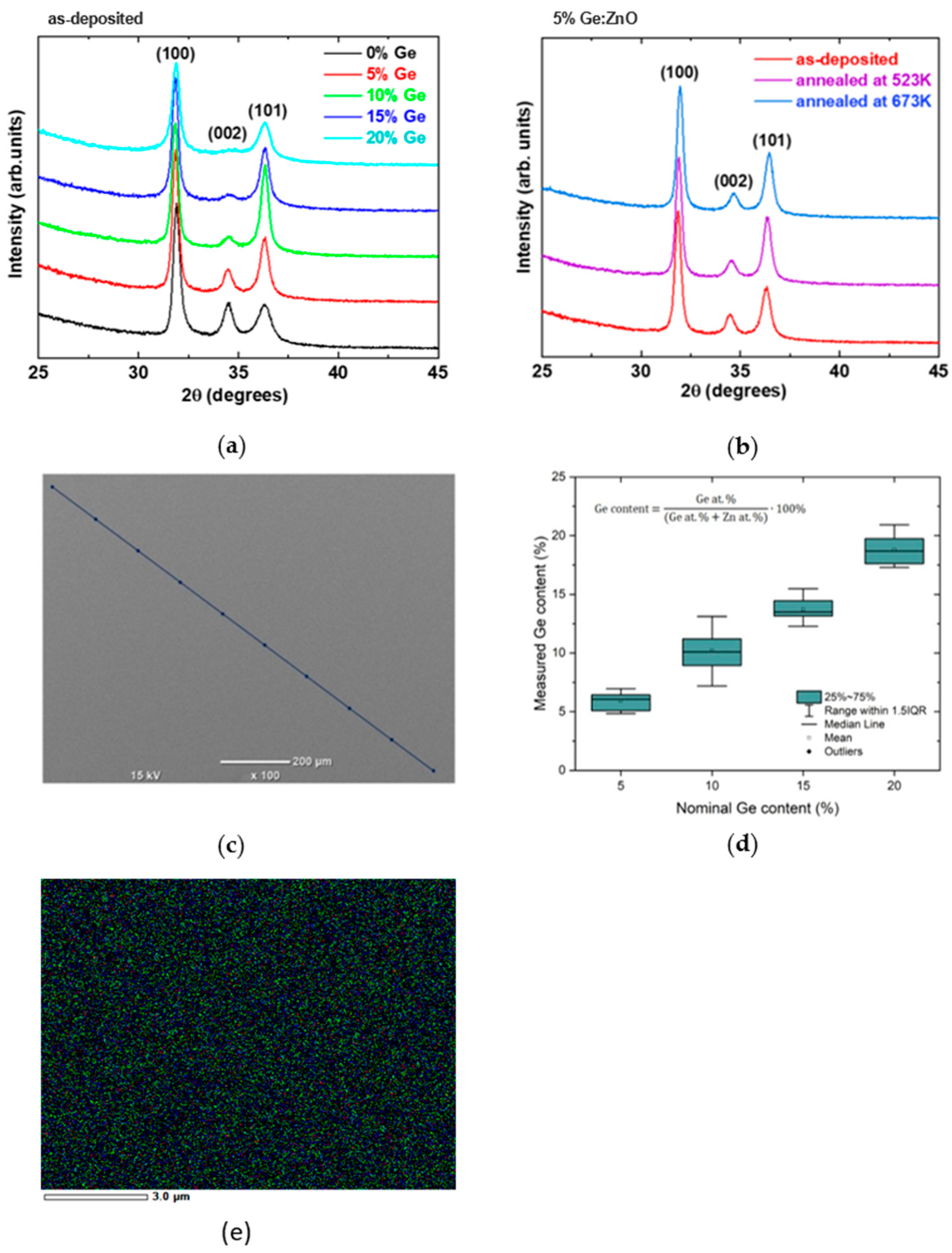
3.1. Structural Characterization

The XRD patterns of the as-deposited films are shown in Figure 1a. The reflections in the XRD patterns can be indexed using the reference (01-070-8072 ICSD). The as-deposited films exhibit the Wurtzite structure, which has been reported previously [34]. In the XRD pattern, only three strong reflections can be observed in the 2θ range between 31° and 39°. These reflections belong to the (100), (002), and (101) planes, respectively. When the ratio of the Ge pulse in the supercycle from 5% to 20% is increased, there is a gradual reduction in the intensity of the (100) peaks of the as-deposited films, which indicates a decrease in the crystallinity. The same trend is also present in the (002) peak, which clearly suggests a decrease in the long-range ordering of the atoms in the lattice or an increase in texture. Similar effects have also been reported previously [34]. The peculiar changes in diffraction maxima intensity, especially (002) and (101), are most likely connected with the texture of the films. While the exact mechanism of texture formation is, at this point, hard to determine, it is clearly related to the amount of germanium in the film.
Figure 1b shows XRD patterns to demonstrate the influence of annealing an as-deposited film that contains 5% Ge from the ALD supercycle. Annealing of the film at 523 K and 673 K did not cause significant changes in the XRD pattern. A minor increase in the intensity of peaks suggests an increase in the crystallinity of the films, which is expected for high-temperature annealing and was later confirmed by XPS spectra analysis.
The EDS measurements have been performed at 10 locations on the diagonal of the SEM image (Figure 1c). This image does not reveal any details regarding morphology. This suggests that the sample is very uniform. Therefore, high-resolution analyses using AFM are necessary. Slight deviations in composition have been observed, which could be attributed to the accuracy of the EDS method. However, the trend reflects well the desired nominal Ge concentration in the samples (Figure 1d, Table 1). The deviations from the desired thickness of the films (100 nm) come from the fact that, during ALD deposition of Ge-doped ZnO, the growth per cycle parameter (GPC) decreases from ~0.16 nm/c (ZnO) to ~0.10 nm/c for pulse ratio GEME/(GEME + DEZ) = 0.5 in the supercycle, due to the steric hindrance during dopant layer deposition [34], which needed to be compensated by setting a number of supercycles. In our research, the ellipsometric method was used to determine the thickness of ALD deposits. As can be seen, the theoretical value is slightly different from the measured value, most likely due to inaccuracy during compensation for the changing growth per cycle. In all consecutive analyses, the measured value of thickness was employed.
Additionally, the lack of detectable foreign phases, such as Zn2GeO4 reported for Ge-doped ZnO [38], on the XRD patterns in connection with the sequential nature of the ALD method and the relatively small deviations in composition of the samples measured by the EDX method indicate that the obtained film is uniform.
Both point analysis (see Figure 1d) and elemental composition mapping (see Figure 1e) demonstrate the homogeneity of the elemental composition.
As mentioned earlier, SEM analyses (see Figure 1c) do not reveal any morphological details. Therefore, AFM analyses were performed. The obtained opacity is shown in Figure 2. All recorded images represent an area of 10 × 10 µm. The Z axis represents height in nm. Figure 2a shows the topography of pure silicon used as a substrate. Then, Figure 2b,c show the topography of 5% Ge:ZnO before and after annealing, respectively. The next two drawings, i.e., Figure 2d,e, show the topography of 15% Ge:ZnO before and after annealing, respectively.
Detailed results of the roughness analysis are presented in the table below (see Table 2). As can be seen, the roughness does not change statistically significantly after the annealing process. However, the roughness of the samples is much higher than the roughness of the substrate. It is commonly assumed that the deposition of homogeneous layers up to several hundred nanometers using the ALD method is possible. In this case, already at a deposit thickness of 100 nm, we observe an increase in surface defects visible in the form of an increase in sample roughness. It is worth emphasizing that an increase in the share of Ge in the sediment does not affect the increase in roughness; on the contrary, layers containing up to 15% Ge:ZnO have Sa 3 nm lower compared to 5% Ge:ZnO, which in our opinion is a statistically significant difference.
The bonding nature of the atoms was studied using XPS. The total concentration of the elements at the sample surface was measured with the survey spectra shown in Figure 2a, and the absolute spectra of each constituent element, i.e., Zn 2p, O 1s and Ge 3d in the compound are shown in Figure 2b–d. Table 3 shows the percentage composition of all the elements present in the survey spectra. Considering the energy of the probing beam, the composition of the film is obtained from the first 5–10 nm of the surface. The different components in each peak obtained after peak fitting correspond to different chemical states of that particular element, and the peak assignments of these states were undertaken according to the databases [43,44].
It is worth noting here that the Ge:ZnO deposition process each time ended with a ZnO deposition cycle. Therefore, the results of the elemental composition analyses presented in Table 1 and Table 3 differ from each other. It should be taken into account that the depth of analysis using the XPS method is less than 5 nm, while EDS is up to 3 µm, depending on the material and measurement parameters. Therefore, XPS results will always be underestimated in such cases. Furthermore, the amount of carbon is different for the measured samples, as it mostly comes from surface contamination rather than traces of unreacted precursor. Noteworthy, the Ge/Zn ratio is the same for both measurements.
From the compositions obtained from survey spectra, it can be observed that the amounts of both Zn and O are higher on the surface of the film that was subjected to air annealing. The reason for a higher O content can be due to the availability of atmospheric oxygen during the annealing process. Furthermore, the surface concentrations obtained using XPS are different than those from EDX due to the layered way of introducing dopant using the ALD technique and the surface vs. in-depth sensitivity of XPS and EDS, respectively.
The absolute spectra of O1s (shown in Figure 3b) can be deconvoluted into components A, B, C and D that refer to oxygen vacancies, oxygen in the oxide lattice, hydroxyl or short oxidized aliphatic groups on the surface and adsorbed water, respectively. Annealing leads to a decrease in oxygen vacancies from 14.3% to 3% and an increase in oxygen in the ZnO lattice from 55% to 65%, which can be explained by filling the vacancies by absorbing the oxygen from the oxygen-rich (~20%) annealing atmosphere. Additionally, the annealing process led to the transformation from OH to an oxide-terminated surface or filling of the oxygen vacancies. Thus, a peak shift to the right is observed compared to as-deposited sample.
The absolute spectra of Zn 2p shown in Figure 3c appear as a doublet, and they can be deconvoluted into three components that represent E-zinc from the unreacted precursor (Zn-C) or zinc in the vicinity of oxygen vacancy (Zn-VO), F-zinc in the ZnO lattice, and G-zinc connected to hydroxyl groups at the surface. The large share of Zn-OH in the as-deposited sample can be explained by the water termination of the ALD process. Annealing led to a transformation from OH to an oxide-terminated surface or filling of the oxygen vacancies, thus decreasing the share of the A component and increasing the share of the B component.
The Ge 3d spectra (Figure 3d) can be deconvoluted into components H and I, corresponding to unstoichiometric oxide or unreacted Ge precursor (Ge2+), and germanium oxide in the zinc oxide lattice (Ge4+), respectively. Annealing leads to shifting of the spectra towards lower binding energies, which can be connected with a recrystallization of the structure, also visible on the Zn 2p and O 1s spectra, and the formation of a GeO2-like phase, which was, however, not recognizable on the XRD patterns.
On Figure 3a, the XPS survey spectrum also reveals a significant carbon contribution in both the as-deposited and annealed samples. As is known, XPS is a highly sensitive method with an analysis depth not exceeding 1–10 nm [45]. Therefore, this technique is susceptible to surface contamination. The sample annealed at 523 K exhibits a slightly lower carbon content compared to the as-deposited sample, confirming that carbon is predominantly of surface contamination origin rather than being an unreacted precursor.

3.2. Annealing Kinetics

To establish the annealing time needed to achieve equilibrium state, eight samples of 5% Ge:ZnO thin films from one deposition batch were annealed in dry air flow at 523 K for different times ranging from 5 min to 4 h. The results of electrical measurements, i.e., conductivity, carrier concentration and mobility, indicate rapid changes in the first 40 min of annealing. The equilibrium state under the annealing conditions was reached after approximately 2 h (Figure 4). After this time, the properties remained constant in time within reasonable measurement uncertainty. Based on the observed behavior, the final time of annealing was set to 4 h to ensure proper stabilization of the sample.

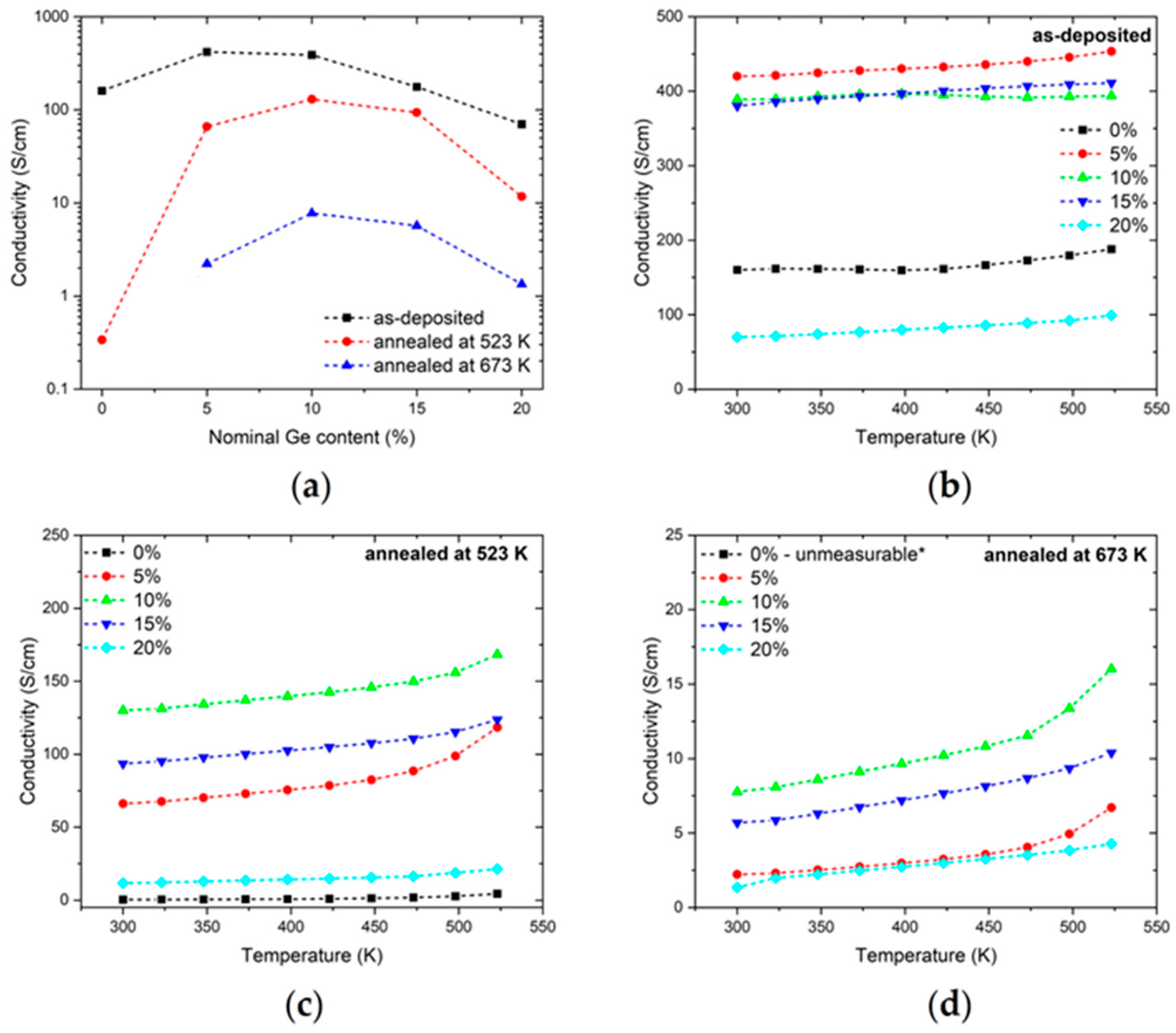
3.3. Annealing in Air

The results of electrical properties measurements, i.e., conductivity (Figure 5), carrier concentration (Figure 6), and mobility (Figure 7), performed up to 523 K are shown for as-deposited samples and samples annealed at 523 K or 673 K.
In the as-deposited samples, one can see that the conductivity maximum is at 5%, which results from increased carrier concentration from ~6 × 1019 cm−3 up to ~3 × 1020 cm−3 for 0 and 5% Ge-doped samples, respectively. For higher Ge dopant concentrations, the carrier concentration remains at the same level, while the carrier mobility tends to decrease, thus implying increasing charge carrier scattering and leading to decreased conductivity. The results presented herein, e.g., the peak conductivity of the as-deposited samples being 5% Ge:ZnO or the decrease of mobility with increasing Ge content, are in agreement with observations and conclusions drawn by Chalker et al. [34] and elaborated by Zhu et al. [35].
In the case of annealed samples, the maximum conductivity decreases roughly 3 and 40 times after annealing at 523 K and 673 K, respectively, relative to the as-deposited samples. This change is greatly influenced by the change in carrier concentration and only slightly by the changes in carrier mobility, especially in the case of strongly doped samples (>10% Ge). Furthermore, the carrier concentrations are not influenced by temperature, and the slight positive correlation between conductivity and temperature was identified to be connected with an increase in carrier mobility, especially in the case of the undoped and annealed sample, which has a relatively low carrier concentration.
Due to the fact that the samples are sensitive to annealing in air (as shown in Figure 4), and the deposition procedure requires the operator to remove them from a hot reactor chamber in ambient atmosphere, some deviations from ideal trends are possible, for example, the slight drop in carrier concentration of the 15% Ge:ZnO sample in Figure 6a. However, these changes are smaller than those inflicted by proper annealing, do not contradict general conclusions and are impossible to eliminate with the large-scale ALD equipment used in this study.

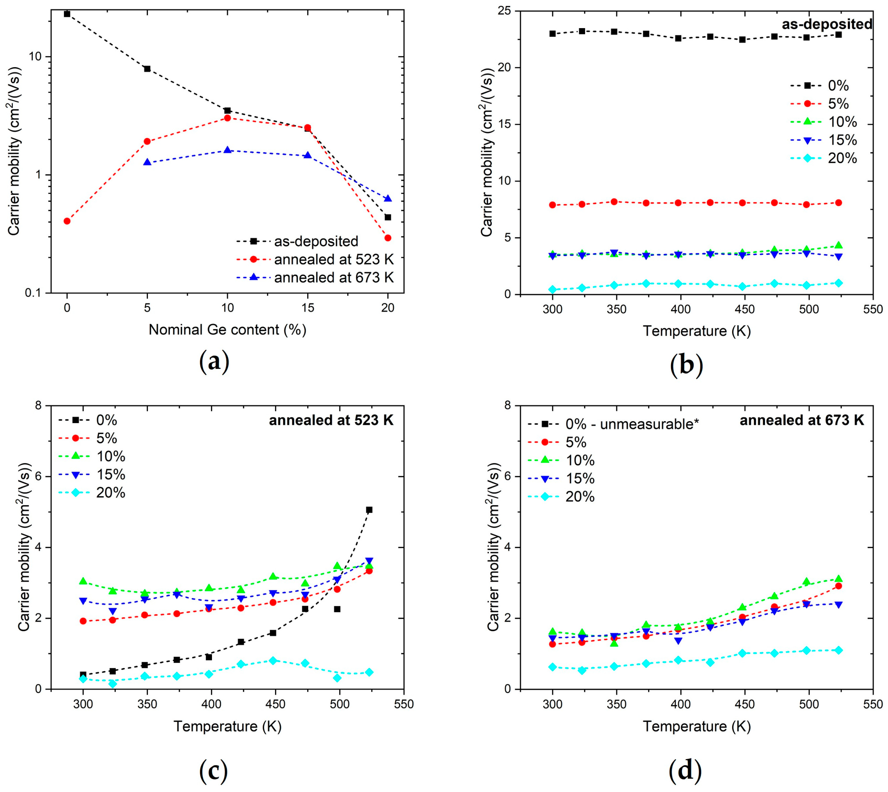
3.4. Discussion of Electronic Properties

Theoretical estimations based on the volume of the ZnO unit cell (a = 3.2495 Å, c = 5.2062 Å, two Zn atoms per unit cell [22]) and the amount of Ge doping, under the assumption that every dopant atom that substitutes Zn (i.e., GeZn) provides two additional electrons (~7.2 × 1021 cm−3), lead to the conclusion that the measured carrier concentration is too low for such a simple doping mechanism to be valid. Furthermore, the carrier concentration decreases significantly from ~5 × 1021 cm−3 to ~2 × 1019 cm−3 for as-deposited samples and samples annealed in air at 673 K, respectively, which should not be the case if Ge was the major charge carrier donor. This also supports the hypothesis that the main contribution to changes in the electrical conductivity does not come only from the Ge doping but rather from other defects, which are more susceptible to annealing conditions. Moreover, the unchanging ratio of Ge4+ and Ge2+ atoms in the structure estimated using the Ge 3d XPS spectra also supports the conclusion that Ge is not the major contributor to annealing-induced changes in carrier concentration. As a result of this reasoning and due to the lack of other phases as evidenced from X Ray diffractograms, it is reasonable to claim that Ge4+, located either in the ZnO lattice, possibly in the vicinity of zinc vacancy and forms charge-neutral GeZn-VZn defect complexes at the grain boundaries [35] or in the form of GeO2 nanograins (especially after annealing), thus making them hard to detect with diffraction methods.
When it comes to the electronic properties of the material, formerly, there was a common belief that oxygen vacancies, while common in ZnO, are deep donors and do not contribute to electronic properties [41]. In 2016, however, a study based on the oxygen isotope self-diffusion in ZnO showed that the oxygen vacancies are responsible for its intrinsic n-type conductivity [46].
The results obtained in this work are in favor of the electronic conductivity mechanism, which is based on oxygen vacancies that act as electron donors. The reasoning behind such claims is as follows: (1) Zinc oxide thin films were fabricated using the ALD method at 200 °C and ~1 mbar of N2 pressure, and because of that, the structure after synthesis is oxygen deficient, i.e., contains oxygen vacancies that contribute electrons to the conduction band and facilitate n-type conductivity. (2) Annealing in air leads to better crystallization of the structure and filling of the oxygen vacancies, which can be related to a decrease in the carrier concentration. These claims are supported by the fact that there are no major changes in the XPS spectra of Zn 2p and Ge 3d while the amount of oxygen vacancies estimated from the XPS spectra of O 1s decreases significantly during annealing.
The argumentation stated above is also in line with the theoretical evaluation of defect formation energy as a function of Fermi level position [41], which leads to Fermi level pinning due to Ge n-type doping. During deposition (in an oxygen-poor atmosphere), the formation energy of oxygen vacancies is negative but increases with the Fermi level position, as opposed to the formation energy of zinc vacancies, which is high and positive but decreases with increasing Fermi level. Since Ge is expected to move the Fermi level up (i.e., add electrons to the system), an equilibrium is reached, and the carrier concentration is stabilized by the amount of oxygen vacancies even at different doping concentrations. During annealing (in an oxygen-rich atmosphere), the formation energy of zinc vacancies is shifted lower, while the formation energy of oxygen vacancies is shifted higher (compared to oxygen-poor conditions), thus leading to fewer electrons being contributed by the oxygen vacancies and the additional effect of electron compensation by charge-neutral ZnGe-VZn defect complexes, thus leading to lower carrier concentrations than in samples that are not annealed. As a result, in either condition, the system opposes drastic shifts of the Fermi level towards higher energies and leads to pinning of the Fermi level.
An alternative explanation based primarily on zinc interstitials that would act as shallow electron donors and, due to the high mobility of Zn above 523 K [47], be annihilated during the annealing process was also considered; however, contrary to the oxygen vacancy filling-based mechanism, it was not supported enough by the XPS analysis.

4. Conclusions

In this work, a series of Ge-doped ZnO thin films were grown by the ALD method in an industrial-scale reactor, and their electrical properties in the as-deposited state and after annealing were investigated. The films’ structure and composition were characterized using XRD, ellipsometry, and SEM EDS, which confirmed that thin films with a thickness of ~100 nm consisting of Ge-doped ZnO were obtained. The samples were subjected to annealing in air at 523 K and 673 K, and their high-temperature electronic properties (electrical conductivity, carrier concentration, and mobility) were measured from room temperature up to 523 K using the Hall effect measurement system, and the observed changes were explained based on XPS and XRD investigations of the materials. The XRD patterns were in all cases very similar and indicated the presence of only one dominant phase—Wurzite ZnO. The XPS spectra analysis revealed, however, that annealing in air leads to a significant decrease in the concentration of oxygen vacancies, implying its strong relation to the electronic properties of this material.
The results presented here are strongly in line with the concept that the oxygen vacancies are electron donors rather than acting like deep-level defects, which could not contribute to the electronic state of the materials. This work also points out that the diffusion of oxygen can occur efficiently for thin films at relatively low temperatures, i.e., 523 K.

Author Contributions

Conceptualization, M.W. and R.P.S.; formal analysis, R.K., K.S. and S.S.; investigation, R.K., K.S., M.M.-W., J.G., G.S., P.Ż. and S.I.; writing—original draft preparation, R.K. and K.S.; writing—review and editing, S.S., M.W. and R.P.S.; visualization, R.K., K.S. and S.S.; supervision, M.W. and R.P.S.; funding acquisition, R.P.S. All authors have read and agreed to the published version of the manuscript.

Funding

This research was funded by the National Center for Research and Development (NCBiR), grant number TANGO-V-C/0014/2021.

Data Availability Statement

Data are contained within the article.

Conflicts of Interest

The authors declare no conflicts of interest.

References

  1. Liu, S.; Li, M.Y.; Su, D.; Yu, M.; Kan, H.; Liu, H.; Wang, X.; Jiang, S. Broad-Band High-Sensitivity ZnO Colloidal Quantum Dots/Self-Assembled Au Nanoantennas Heterostructures Photodetectors. ACS Appl. Mater. Interfaces 2018, 10, 32516–32525. [Google Scholar] [CrossRef]
  2. Li, M.-Y.; Yu, M.; Su, D.; Zhang, J.; Jiang, S.; Wu, J.; Wang, Q.; Liu, S. Ultrahigh Responsivity UV Photodetector Based on Cu Nanostructure/ZnO QD Hybrid Architectures. Small 2019, 15, 1901606. [Google Scholar] [CrossRef]
  3. Zheng, T.; Li, Z.; Chen, J.; Shen, K.; Sun, K. Transitions of Microstructure and Photoluminescence Properties of the Ge/ZnO Multilayer Films in Certain Annealing Temperature Region. Appl. Surf. Sci. 2006, 252, 8482–8486. [Google Scholar] [CrossRef]
  4. Suganthi, K.; Vinoth, E.; Sudha, L.; Bharathi, P.; Navaneethan, M. Manganese (Mn2+) Doped Hexagonal Prismatic Zinc Oxide (ZnO) Nanostructures for Chemiresistive NO2 Sensor. Sens. Actuators B Chem. 2023, 380, 133293. [Google Scholar] [CrossRef]
  5. George, S.M. Atomic Layer Deposition: An Overview. Chem. Rev. 2009, 110, 111–131. [Google Scholar] [CrossRef] [PubMed]
  6. Ovanesyan, R.A.; Filatova, E.A.; Elliott, S.D.; Hausmann, D.M.; Smith, D.C.; Agarwal, S. Atomic Layer Deposition of Silicon-Based Dielectrics for Semiconductor Manufacturing: Current Status and Future Outlook. J. Vac. Sci. Technol. A Vac. Surf. Film. 2019, 37, 060904. [Google Scholar] [CrossRef]
  7. Zaidi, S.J.A.; Basit, M.A.; Park, T.J. Advances in Atomic Layer Deposition of Metal Sulfides: From a Precursors Perspective. Chem. Mater. 2022, 34, 7106–7138. [Google Scholar] [CrossRef]
  8. Dasgupta, N.P.; Meng, X.; Elam, J.W.; Martinson, A.B.F. Atomic Layer Deposition of Metal Sulfide Materials. Acc. Chem. Res. 2015, 48, 341–348. [Google Scholar] [CrossRef]
  9. Witkowski, M.; Starowicz, Z.; Zięba, A.; Adamczyk-Cieślak, B.; Socha, R.P.; Szawcow, O.; Kołodziej, G.; Haras, M.; Ostapko, J. The Atomic Layer Deposition (ALD) Synthesis of Copper-Tin Sulfide Thin Films Using Low-Cost Precursors. Nanotechnology 2022, 33, 505603. [Google Scholar] [CrossRef]
  10. He, Z.; Zhou, Y.; Liu, A.; Gao, L.; Zhang, C.; Wei, G.; Ma, T. Recent Progress in Metal Sulfide-Based Electron Transport Layers in Perovskite Solar Cells. Nanoscale 2021, 13, 17272–17289. [Google Scholar] [CrossRef] [PubMed]
  11. Shen, C.; Yin, Z.; Collins, F.; Pinna, N. Atomic Layer Deposition of Metal Oxides and Chalcogenides for High Performance Transistors. Adv. Sci. 2022, 9, 2104599. [Google Scholar] [CrossRef]
  12. Tynell, T.; Karppinen, M. Atomic Layer Deposition of ZnO: A Review. Semicond. Sci. Technol. 2014, 29, 43001. [Google Scholar] [CrossRef]
  13. Zhao, K.; Xie, J.; Zhao, Y.; Han, D.; Wang, Y.; Liu, B.; Dong, J. Investigation on Transparent, Conductive ZnO:Al Films Deposited by Atomic Layer Deposition Process. Nanomaterials 2022, 12, 172. [Google Scholar] [CrossRef]
  14. Fei, Y.; Li, Y.; Li, Y.; Xie, A.; Li, Y.; Sun, D. Properties Study of ZnO Films Prepared by ALD. J. Mol. Struct. 2022, 1269, 133804. [Google Scholar] [CrossRef]
  15. Kruszyńska, J.; Ostapko, J.; Ozkaya, V.; Surucu, B.; Szawcow, O.; Nikiforow, K.; Hołdyński, M.; Tavakoli, M.M.; Yadav, P.; Kot, M.; et al. Atomic Layer Engineering of Aluminum-Doped Zinc Oxide Films for Efficient and Stable Perovskite Solar Cells. Adv. Mater. Interfaces 2022, 9, 2200575. [Google Scholar] [CrossRef]
  16. Starowicz, Z.; Zięba, A.; Ostapko, J.; Wlazło, M.; Kołodziej, G.; Jakub Szczerba, M.; Putynkowski, G.; Piotr Socha, R. Synthesis and Characterization of Al-Doped ZnO and Al/F Co-Doped ZnO Thin Films Prepared by Atomic Layer Deposition. Mater. Sci. Eng. B 2023, 292, 116405. [Google Scholar] [CrossRef]
  17. Iatsunskyi, I.; Kempiński, M.; Jancelewicz, M.; Załęski, K.; Jurga, S.; Smyntyna, V. Structural and XPS Characterization of ALD Al2O3 Coated Porous Silicon. Vacuum 2015, 113, 52–58. [Google Scholar] [CrossRef]
  18. Myers, T.J.; Throckmorton, J.A.; Borrelli, R.A.; O’Sullivan, M.; Hatwar, T.; George, S.M. Smoothing Surface Roughness Using Al2O3 Atomic Layer Deposition. Appl. Surf. Sci. 2021, 569, 150878. [Google Scholar] [CrossRef]
  19. Dvorak, F.; Zazpe, R.; Krbal, M.; Sopha, H.; Prikryl, J.; Ng, S.; Hromadko, L.; Bures, F.; Macak, J.M. One-Dimensional Anodic TiO2 Nanotubes Coated by Atomic Layer Deposition: Towards Advanced Applications. Appl. Mater. Today 2019, 14, 1–20. [Google Scholar] [CrossRef]
  20. Moehl, T.; Suh, J.; Sévery, L.; Wick-Joliat, R.; David Tilley, S. Investigation of (Leaky) ALD TiO2 Protection Layers for Water-Splitting Photoelectrodes. ACS Appl. Mater. Interfaces 2017, 9, 43614–43622. [Google Scholar] [CrossRef]
  21. Norton, D.P.; Heo, Y.W.; Ivill, M.P.; Ip, K.; Pearton, S.J.; Chisholm, M.F.; Steiner, T. ZnO: Growth, Doping & Processing. Mater. Today 2004, 7, 34–40. [Google Scholar] [CrossRef]
  22. Borysiewicz, M.A. ZnO as a Functional Material, a Review. Crystals 2019, 9, 505. [Google Scholar] [CrossRef]
  23. Kołodziejczak-Radzimska, A.; Jesionowski, T. Zinc Oxide—From Synthesis to Application: A Review. Materials 2014, 7, 2833–2881. [Google Scholar] [CrossRef]
  24. Yang, J.; Park, J.K.; Kim, S.; Choi, W.; Lee, S.; Kim, H. Atomic-Layer-Deposited ZnO Thin-Film Transistors with Various Gate Dielectrics. Phys. Status Solidi A 2012, 209, 2087–2090. [Google Scholar] [CrossRef]
  25. Yang, J.; Bahrami, A.; Ding, X.; Lehmann, S.; Kruse, N.; He, S.; Wang, B.; Hantusch, M.; Nielsch, K. Characteristics of ALD-ZnO Thin Film Transistor Using H2O and H2O2 as Oxygen Sources. Adv. Mater. Interfaces 2022, 9, 2101953. [Google Scholar] [CrossRef]
  26. Shih, Y.T.; Wu, M.K.; Li, W.C.; Kuan, H.; Yang, J.R.; Shiojiri, M.; Chen, M.J. Amplified Spontaneous Emission from ZnO in N-ZnO/ZnO Nanodots-SiO2 Composite/p-AlGaN Heterojunction Light-Emitting Diodes. Nanotechnology 2009, 20, 165201. [Google Scholar] [CrossRef]
  27. Chen, M.-J.; Yang, J.-R.; Shiojiri, M. ZnO-Based Ultra-Violet Light Emitting Diodes and Nanostructures Fabricated by Atomic Layer Deposition. Semicond. Sci. Technol. 2012, 27, 74005. [Google Scholar] [CrossRef]
  28. Zhao, J.; Wang, Y. Surface Modifications of Li-Ion Battery Electrodes with Various Ultrathin Amphoteric Oxide Coatings for Enhanced Cycleability. J. Solid State Electrochem. 2013, 17, 1049–1058. [Google Scholar] [CrossRef]
  29. Szabó, Z.; Volk, J.; Horváth, Z.E.; Medveczky, Z.; Czigány, Z.; Vad, K.; Baji, Z. Atomic Layer Deposition and Annealing of Ga Doped ZnO Films. Mater. Sci. Semicond. Process 2019, 101, 95–102. [Google Scholar] [CrossRef]
  30. Nam, T.; Lee, C.W.; Kim, H.J.; Kim, H. Growth Characteristics and Properties of Ga-Doped ZnO (GZO) Thin Films Grown by Thermal and Plasma-Enhanced Atomic Layer Deposition. Appl. Surf. Sci. 2014, 295, 260–265. [Google Scholar] [CrossRef]
  31. Hong, C.; Kang, K.M.; Kim, M.; Wang, Y.; Kim, T.; Lee, C.; Park, H.H. Structural, Electrical, and Optical Properties of Si-Doped ZnO Thin Films Prepared via Supercycled Atomic Layer Deposition. Mater. Sci. Eng. B 2021, 273, 115401. [Google Scholar] [CrossRef]
  32. Geng, Y.; Xie, Z.Y.; Yang, W.; Xu, S.S.; Sun, Q.Q.; Ding, S.J.; Lu, H.L.; Zhang, D.W. Structural, Optical, and Electrical Properties of Hf-Doped ZnO Films Deposited by Atomic Layer Deposition. Surf. Coat. Technol. 2013, 232, 41–45. [Google Scholar] [CrossRef]
  33. Ellmer, K.; Bikowski, A. Intrinsic and Extrinsic Doping of ZnO and ZnO Alloys. J. Phys. D Appl. Phys. 2016, 49, 413002. [Google Scholar] [CrossRef]
  34. Chalker, P.R.; Marshall, P.A.; King, P.J.; Dawson, K.; Romani, S.; Williams, P.A.; Ridealgh, J.; Rosseinsky, M.J. Atomic Layer Deposition of Germanium-Doped Zinc Oxide Films with Tuneable Ultraviolet Emission. J. Mater. Chem. 2012, 22, 12824–12829. [Google Scholar] [CrossRef]
  35. Zhu, W.; Kammuri, T.; Kitamura, S.; Sturaro, M.; Martucci, A.; Pezzotti, G. Structure and Composition Evaluation of Heavily Ge-Doped ZnO Nanocrystal Films. J. Phys. D Appl. Phys. 2018, 51, 085302. [Google Scholar] [CrossRef]
  36. Zhou, Z.; Zheng, Y.; Yang, Y.; Zhang, W.; Zou, M.; Nan, C.-W.; Lin, Y.-H. Enhanced Thermoelectric Performance of ZnO-Based Thin Films via Interface Engineering. Crystals 2022, 12, 1351. [Google Scholar] [CrossRef]
  37. Li, L.; Fang, L.; Zhou, X.J.; Liu, Z.Y.; Zhao, L.; Jiang, S. X-ray Photoelectron Spectroscopy Study and Thermoelectric Properties of Al-Doped ZnO Thin Films. J. Electron Spectrosc. Relat. Phenom. 2009, 173, 7–11. [Google Scholar] [CrossRef]
  38. Yu, Y.S.; Kim, G.Y.; Min, B.H.; Kim, S.C. Optical Characteristics of Ge Doped ZnO Compound. J. Eur. Ceram. Soc. 2004, 24, 1865–1868. [Google Scholar] [CrossRef]
  39. Sypniewska, M.; Szczesny, R.; Popielarski, P.; Strzalkowski, K.; Derkowska-Zielinska, B. Structural, Morphological and Photoluminescent Properties of Annealed ZnO Thin Layers Obtained by the Rapid Sol-Gel Spin-Coating Method. Opto-Electron. Rev. 2020, 28, 182–190. [Google Scholar] [CrossRef]
  40. Ghosh, H.; Sadeghimakki, B.; Sivoththaman, S. Enhancement of UV Emission and Optical Bandgap of ZnO Nanowires via Doping and Post-Growth Annealing. Mater. Res. Express 2020, 7, 035013. [Google Scholar] [CrossRef]
  41. Janotti, A.; Van De Walle, C.G. Fundamentals of Zinc Oxide as a Semiconductor. Rep. Progress. Phys. 2009, 72, 126501. [Google Scholar] [CrossRef]
  42. ISO 15472:2010; Surface Chemical Analysis—X-ray Photoelectron Spectrometers—Calibration of Energy Scales. ISO: Geneva, Switzerland, 2010.
  43. Moulder, J.F.; Stickle, W.F.; Sobol, W.M.; Bomben, K.D. Handbook of X-ray Photoelectron Spectroscopy. Perkin-Elmer Corp. 1992, 40, 221. [Google Scholar]
  44. NIST. X-ray Photoelectron Spectroscopy Database. In NIST Standard Reference Database Number 20; National Institute of Standards and Technology: Gaithersburg, MD, USA, 2000; p. 20899. [Google Scholar]
  45. Omidi, M.; Fatehinya, A.; Farahani, M.; Akbari, Z.; Shahmoradi, S.; Yazdian, F.; Tahriri, M.; Moharamzadeh, K.; Tayebi, L.; Vashaee, D. 7—Characterization of Biomaterials. In Biomaterials for Oral and Dental Tissue Engineering; Tayebi, L., Moharamzadeh, K., Eds.; Woodhead Publishing: Cambridge, UK, 2017; pp. 97–115. ISBN 978-0-08-100961-1. [Google Scholar]
  46. Liu, L.; Mei, Z.; Tang, A.; Azarov, A.; Kuznetsov, A.; Xue, Q.-K.; Du, X. Oxygen Vacancies: The Origin of n-Type Conductivity in ZnO. Phys. Rev. B 2016, 93, 235305. [Google Scholar] [CrossRef]
  47. Ke, L.; Lai, S.C.; Ye, J.D.; Kaixin, V.L.; Chua, S.J. Point Defects Analysis of Zinc Oxide Thin Films Annealed at Different Temperatures with Photoluminescence, Hall Mobility, and Low Frequency Noise. J. Appl. Phys. 2010, 108, 084502. [Google Scholar] [CrossRef]
Figure 1. XRD patterns of (a) Ge:ZnO thin films after deposition at 473 K. (b) Influence of annealing at 523 K and 673 K on XRD patterns of 5% Ge:ZnO. (c) Example of the EDS analysis along the line. (d) Nominal and measured Ge content based on EDS results. (e) EDS mapping of the surface of the 15% Ge:ZnO sample.
Electronics 13 00554 g001
Figure 2. AFM analysis of the samples: (a) Si substrate; (b) 5% Ge:ZnO; (c) 5% Ge:ZnO after the annealing process; (d) 15% Ge:ZnO; (e) 15% Ge:ZnO after the annealing process.
Electronics 13 00554 g002
Figure 3. XPS (a) survey spectra, (b) O1s spectra, (c) Zn 2p spectra, and (d) Ge 3d spectra for as-deposited (bottom part) and annealed-at-523 K (top part) 5% Ge:ZnO samples.
Electronics 13 00554 g003
Figure 4. Time-dependent (a) conductivity, (b) carrier concentration, and (c) carrier mobility of the 5% Ge:ZnO sample during annealing in dry air flow at 523 K. The samples reach the equilibrium state after approximately 120 min. The dashed lines serve as guides for the eye.
Electronics 13 00554 g004
Figure 5. (a) Room-temperature conductivity of as-deposited and annealed samples as a function of nominal Ge content. The temperature dependency of the conductivity of (b) the as-deposited sample and (c) the sample annealed in dry air flow at 523 K or (d) 673 K. Dashed lines serve as guides for the eye. * The measurement of the undoped sample annealed at 673 K was invalid due to the sample resistance of the instrument being too high.
Electronics 13 00554 g005
Figure 6. (a) Room-temperature carrier concentration of as-deposited and annealed samples as a function of nominal Ge content. The temperature dependency of the carrier concentration of (b) the as-deposited sample and (c) the sample annealed in dry air flow at 523 K or (d) 673 K. Dashed lines serve as guides for the eye. * The measurement of the undoped sample annealed at 673 K was invalid due to the sample resistance of the instrument being too high.
Electronics 13 00554 g006
Figure 7. (a) Room-temperature carrier mobility of as-deposited and annealed samples as a function of nominal Ge content. The temperature dependency of the carrier mobility of (b) the as-deposited sample and (c) the sample annealed in dry air flow at 523 K or (d) 673 K. Dashed lines serve as guides for the eye. * The measurement of the undoped sample annealed at 673 K was invalid due to the sample resistance of the instrument being too high.
Electronics 13 00554 g007
Table 1. The elemental composition and thickness of films deposited on the Si wafer determined using EDS and the ellipsometry method, respectively.
Nominal Ge Content (%)Chemical Composition (at. %)Nominal Ratio Ge/(Zn + Ge) (%)Thickness (nm)
OZnGe
069.9 ± 0.830.1 ± 0.8--103
570.4 ± 0.827.8 ± 0.81.8 ± 0.26.197
1069.4 ± 1.327.5 ± 1.53.1 ± 0.510.1116
1569.5 ± 1.326.3 ± 1.34.2 ± 0.213.8114
2070.8 ± 0.823.7 ± 0.65.5 ± 0.418.8111
Table 2. Roughness analysis of analyzed samples using the AFM method.
SampleRoughness Average (Sa) [nm]
Si wafer0.5
5% Ge:ZnO13.5
5% Ge:ZnO annealed13.6
15% Ge:ZnO10.6
15% Ge:ZnO annealed8.3
Table 3. Concentration of the elements at the surface of the 5% Ge:ZnO sample determined using the XPS method.
5% Ge:ZnOChemical Composition (at. %)
ZnGeOC
As-deposited41.70.8440.716.7
Annealed at 523 K43.450.8743.7511.93
Disclaimer/Publisher’s Note: The statements, opinions and data contained in all publications are solely those of the individual author(s) and contributor(s) and not of MDPI and/or the editor(s). MDPI and/or the editor(s) disclaim responsibility for any injury to people or property resulting from any ideas, methods, instructions or products referred to in the content.

