Abstract
The capacitor mismatch among diverse defects caused by variations in the manufacturing process significantly affects the linearity of the capacitor array used to implement the capacitive digital-to-analog converter (CDAC) in the successive-approximation register (SAR) analog-to-digital converter (ADC). Accordingly, the linearity of the SAR ADC is limited by that of capacitor array, resulting in serious yield loss. This paper proposes an efficient foreground self-calibration technique to enhance the linearity of the SAR ADCs by mitigating the capacitor mismatch based on the split ADC architecture along with variable capacitors. In this work, two ADC channels (i.e., ADC1 and ADC2) for the split ADC architecture include their capacitive DACs (CDACs) whose binary-weighted capacitor arrays consist of variable capacitors. A charge-sharing SAR ADC is used for each ADC channel. In the normal operation mode, their digital outputs are averaged to be the final ADC output, as in a conventional split ADC. In the calibration mode, every single binary-weighted capacitor for the two ADCs is sequentially calibrated by making parallel or/and antiparallel connection among two or thee capacitors from the two channels. For instance, because the capacitors of the CDACs ideally exhibit the binary-weighted relation as , the variable capacitor of ADC1 can be updated to be closest to the sum of of ADC1 and of ADC2 for the calibration. For the process, the two capacitor arrays of the two ADCs can be reconfigured to be connected to each other, so that the of ADC1 can be connected with two of the of ADC1 and ADC2 in antiparallel. The two voltages at the top and the bottom plates of the CDAC are compared by a comparator of ADC1, and the comparison results are used to update . This process is iterated, until is in agreement with the sum of two of . Finally, all the capacitors can be calibrated in this way to have the binary-weighted relation. The simulation results based on the proposed work with a split SAR ADC model verified that the proposed technique can be practically used, by showing that the total harmonic distortion and the signal-to-noise-and-distortion ratio were enhanced by dB and dB, respectively.
1. Introduction
The fourth industrial revolution connects more smart devices, making intelligent networks of things which can communicate to each other, i.e., the internet of things. Mobile devices comprising a large proportion of the smart device require a high power efficiency of circuit components included in their system [1,2,3]. Due to the benefit of low power consumption, the successive-approximation register (SAR) analog-to-digital converter (ADC) among different ADC architectures has been highly attractive for ultra-low power applications such as mobile devices [4], and it can achieve high resolution and accuracy as well [5].
The SAR ADC consists of a capacitive digital-to-analog converter (CDAC), including binary-weighted capacitors, a comparator, and the SAR logic [5]. The capacitor mismatch among various defects caused by the manufacturing process variations negatively impacts on the linearity of the binary-weighted capacitors in the SAR ADC. Thus, the linearity of the SAR ADC is limited by that of a capacitor array, resulting in serious yield loss [6]. Therefore, the SAR ADC architecture suffers from the capacitor mismatch issue.
A straightforward solution to mitigate the capacitor mismatch is to simply increase the dimensions of the binary-weighted capacitors. It may be, however, impractical, because this method can degrade the ADC performances in different aspects, such as a decrease in sampling speed, an increase in area overhead, a higher power dissipation, and more [7].
There have been attempts to overcome mismatch issues of ADCs as follows. In [8], a calibration-purpose capacitor is added to the capacitor array of the CDAC, and so it is used to alleviate the capacitor mismatches. However, it may cause an increase in area overhead of the CDAC, and it can also introduce the complexity in the layout of an ADC. In [9], a lookup table is generated to provide the statistical mapping relation between the ADC nominal outputs and actual outputs degraded by different mismatches. Then, gain mismatches among sub-ADCs are calibrated using this mapping relation. This method, however, requires a long time to generate the lookup table, and also demands a huge memory space for the statistical mapping process data. In [10], the output signal differences between two identical ADCs (i.e., split ADC) are considered as an error, and then the output weight parameters are digitally updated by a genetic algorithm to reduce the errors of an ADC. However, the output difference is not sufficient to represent errors caused by the mismatches, if both ADCs have similar mismatches to be similar outputs [11,12]. The shuffling scheme [13] was employed to a CDAC to avoid this issue, where different unit capacitors were randomly set to be used for different bits in each conversion. However, this method causes high complexity in circuity connections, and it may decrease the conversion speed [12]. In [14], capacitor mismatches of a CDAC in a SAR ADC are calibrated using metal–oxide–semiconductor (MOS) capacitors (MOSCAPs) as a variable capacitor along with a dummy unit capacitor for their calibration purpose. All the capacitors of the CDAC are replaced with the MOSCAPs, and the capacitance of each capacitor is compared with the capacitance sum of the next-smaller capacitors. However, this comparison process requires complicated connections among those capacitors and an additional calculation process, as the resolution of an ADC increases.
This paper proposes a promising self-calibration technique to significantly improve the performances of SAR ADCs by alleviating the capacitor mismatches based on the split ADC architecture with variable capacitors. The aim of this work is to achieve a high calibration accuracy by overcoming the drawback of a conventional split ADC [10].
2. Review of Split ADC Architecture
This section discusses how a conventional split ADC architecture works, and analyzes its benefits and limitations.
2.1. Configuration
A conventional split ADC is configured as shown in Figure 1 [10]. An ADC input signal is applied to two identical ADCs, i.e., ADC1 and ADC2, at the same time. Their outputs, and are fed to the bit weight functions, and in order to be multiplied by the weights, and which are initially unity. In the output process module, the ADC outputs, and are averaged to be which is then used as the normal operation output, while the output difference is applied to the weight updater module as an error between two ADCs. An adaptive algorithm such as a least mean square (LMS) updates and based on in the weight updater, as shown in (1):
where n indicates the sample index, and represents the LMS step size. and are then properly multiplied by the next outputs, and in and . This process is iterated, until is identical to .
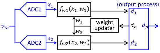
Figure 1.
Configuration of conventional split ADC.
2.2. Considerations
There are several benefits of the split ADC architecture, which are explained as follows. Each ADC channel occupies half the original ADC area, and thus, a split ADC does not require a larger area. In addition, each channel has half of the capacitance where is used for the original ADC, and it may also alleviate the noise at the output by the average process [10].
However, the output difference is not sufficient to represent the mismatch between two ADC channels if both channel outputs include similar errors with the same polarity [11,12], i.e., if and , then . Accordingly, (1) results in (2). The bit weights are, thus, not updated, thereby masking mismatches and degrading calibration accuracy.
This issue can be observed from the simulation results in Figure 2 and Table 1; one model has similar mismatches between their two channels, and the other one does not. The model with this issue exhibited highly nonlinear results, compared to those of the other model without the issue.
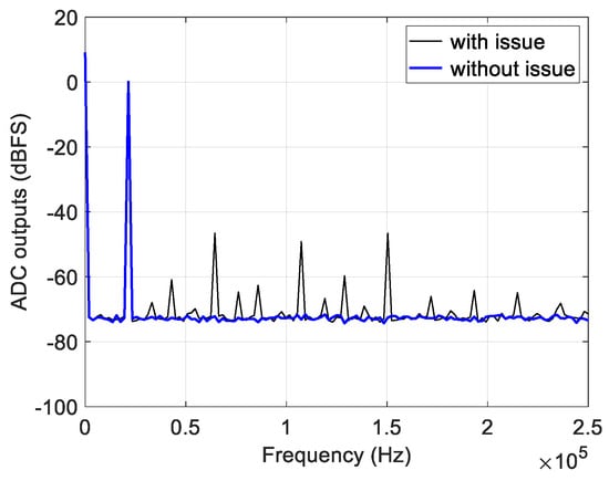
Figure 2.
Spectral responses from simulation of conventional split ADCs with and without issue.

Table 1.
Simulation results of conventional split ADCs with and without issue.
3. Proposed Scheme
This work proposes an efficient foreground self-calibration scheme to enhance the performances of the SAR ADC by mitigating the capacitor mismatches using variable capacitors. As a result, this work overcomes the drawback of a conventional split ADC, as discussed in Section 2.
3.1. Configuration
The proposed work can be simply configured by employing the split ADC platform, as shown in Figure 3a which is derived from Figure 1. The two ADC channels (i.e., ADC1 and ADC2) and the output average process highlighted in blue in a conventional split ADC shown in Figure 1 are employed in this work, because the proposed work does not require an adaptive algorithm using , which is fundamentally required for a conventional split ADC. Thus, the proposed work uniquely uses the two ADC channels for our calibration purpose. Those two ADC channels provide an efficient platform to allow the proposed calibration unit (i.e., cal unit) to calibrate each capacitor using a few reference capacitors, resulting in a much simpler process.The binary-weighted capacitors in the CDAC of each ADC are implemented using the MOSCAP, which is a type of variable capacitor, wherein if a capacitance control signal, , is applied to the MOSCAP, then the MOSCAP is set to its corresponding capacitance. The higher the value of , the lower the capacitance for the MOSCAP is set. Essentially, the MOSACAP is a voltage-controlled variable capacitor. The cal unit consists of two processes, the linear search process for the calibration and the voltage generation (by an embedded voltage generator), to apply the aforementioned to the MOSCAP, as shown in Figure 3c. This work is not limited to a specific architecture of the voltage generation circuit, as long as the correct value of can be generated. Thus, the charge-based voltage generator can be employed from [14]. An 8-bit ADC is used as an example for better understanding of this concept, and the proposed work can simply be applied to a higher resolution of the ADC.
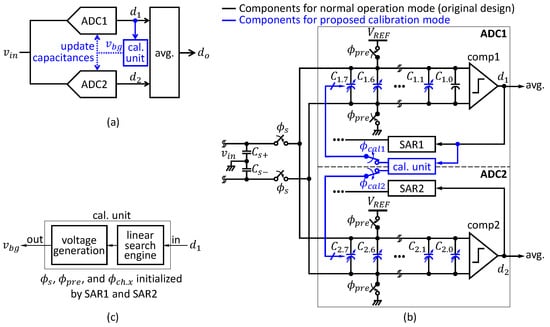
Figure 3.
(a) Configuration of proposed work, (b) proposed foreground self-calibration based on split CS-SAR ADC, and (c) cal unit embedded in (b).
The proposed work in Figure 3a can be realized as shown in Figure 3b. A charge-sharing (CS)-SAR ADC [15] with differential inputs is used for both ADC1 and ADC2, each of which consists of a track/hold stage (omitted in Figure 3b for simplicity), a sample stage ( and ), a CDAC (), and a comparator (comp1 or comp2).
The convention in the CDAC represents either a binary-weighted capacitor or capacitance in contexts, and its subscript indicates each ADC channel index (i.e., 1 or 2), and another subscript x represents each capacitor index in the CDAC (e.g., 0–7 for an 8-bit ADC). Thus, ideally, , , …, , where is a unit capacitor. In addition, is open to make connections between the top and bottom plates of ADC1 and those of ADC2. For each binary-weighted capacitor in a conventional CS-SAR ADC, there are two internal switches, , for each , as depicted in Figure 4a,b [15]. As shown in Figure 4b, those two switches allow us to make a connection between each and their top or bottom plate, resulting in either a parallel () or antiparallel () connection of . We call those two switches, , para-switches for convenience. In addition, a practical capacitance can be modeled as a capacitance combined with an ideal capacitance , and and , which are the parasitic capacitances occurring on the top and bottom plates, respectively [16].
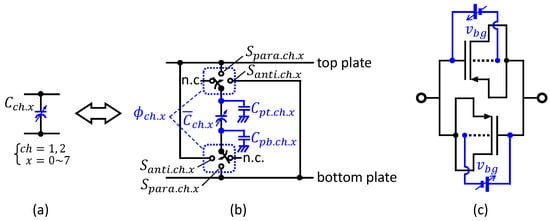
Figure 4.
(a) Variable and binary-weighted capacitor symbol used in Figure 3b represents (b) a capacitor with para-switches, and it can be realized using (c) a variable MOSCAP.
Different types of the capacitor to be used for a CDAC can be considered. While metal–oxide–metal (MOM) capacitors have good linearity, they exhibit a low capacitance density because of the thick oxide layer. In addition, metal-isolation-metal (MIM) and poly-isolation-poly (PIP) capacitors show good linearity and high capacitance density due to the thin oxide layer; however, those require additional masks and more fabrication steps, thereby increasing manufacturing cost. On the other hand, MOSCAPs have a high capacitance density, which need no additional mask processes. With regard to the structure of the MOSCAP, it introduces capacitance between a bulk and a gate of the metal–oxide–semiconductor field-effect transistor (MOSFET) as shown in Figure 4c, and the gate and the source (connected with the drain) are two terminals of a variable MOSCAP. Then, increasing the input voltage, , between the bulk and the gate almost linearly decreases the capacitance between their two terminals, resulting in a MOSCAP as a variable capacitor. Those capacitors, however, suffer from nonlinearity; a MOSCAP differently operates in three operation regions divided on the basis of voltage values across the MOSCAP, where its capacitance varies with the voltage value across the MOSCAP in the depletion region, while it is overall constant in the accumulation and inversion regions. As mentioned in Section 1, in [14], all the capacitors of the CDAC are replaced with variable MOSCAPs, as shown in Figure 4c, by carefully using the MOSCAPs in the inversion region, and thus, a SAR ADC is calibrated based on the binary-weight relation among capacitors along with a dummy unit capacitor for their calibration purpose.
In the proposed work, the variable MOSCAPs employed from [14] are fully charged in the precharge step. Then, because the passive CDAC of the CS SAR ADC is not connected with any power source and also has no connection with external circuitry—assuming a comparator has high impedance at its input terminal—the same amount of the net charges in the capacitors are retained until the sampling step is completed. Thus, the MOSCAPs stay in the inversion region during the calibration process. The variable MOSCAP shown in Figure 4c is discussed in detail in [14,16]. The aim of this work is to accomplish a highly accurate calibration methodology by overcoming the drawback of a conventional split ADC, using a variable capacitor and its input voltage generator employed from [14] in cal unit. In addition, the variable capacitors used for the cal unit can be a capacitor array as well as a voltage-controlled capacitor (e.g., variable MOSCAP, varicap, and more). In fact, proposing a new variable capacitor along with its input voltage generator is not trivial, and thus, it is out of the scope of this work.
To summarize, the components for this work are highlighted in blue in Figure 3b, such as variable capacitor-based arrays of the CDAC, the nodes , cal unit, and switches . For efficiency, a set of the track/hold stage and a set of the sample stage, which is designed for each of the two ADC channels in a conventional split ADC, are merged into a single set, which can be shared by the two ADCs for this work, so that ADC1 and ADC2 can use the same exact input stage, as shown in Figure 3b.
3.2. Calibration Process
The procedure for the proposed foreground self-calibration is discussed in detail in this section. The proposed scheme is performed in two sequential steps, (1) precharge and (2) capacitance calibration, and the full process is operated by cal unit.
For the precharge step (i.e., the first step), the split CS-SAR ADC shown in Figure 3b is reconfigured into that shown in Figure 5, by performing the following: is open to disconnect the sampling stage (i.e., and ) from the CDAC for both the channels. is closed to provide the charges to all the binary-weighted capacitors. The para-switches of all the capacitors are then connected to their as shown in Figure 4b, and comp1 and comp2 are disabled. Finally, all the binary-weighted capacitors are fully precharged by .
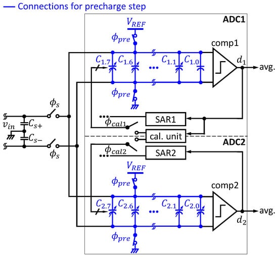
Figure 5.
Precharge step.
For the capacitance calibration (i.e., the second step), all the binary-weighted capacitors are sequentially calibrated in order from the least-significant-bit (LSB) capacitor to the most-significant-bit (MSB) capacitor, as listed in Table 2, thereby completing all the capacitors in the binary-weighted relation. To better illustrate this, the first two sequences in Table 2 are explained using Figure 5, Figure 6 and Figure 7 and Table 2 in detail as an example, instead of describing the generalized procedure.
Table 2.
Capacitors participating in each calibration sequence.
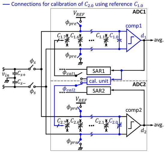
Figure 6.
Capacitance calibration step for the first calibration sequence in Table 2.
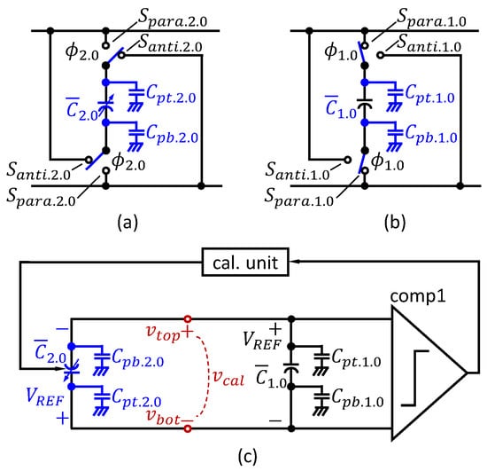
The first calibration sequence of Table 2 calibrates using as a reference capacitor, without any change in after its fabrication, as shown in Figure 6. Firstly, the LSB capacitors of each ADC channel (i.e., and ) are connected to their top and bottom plates in antiparallel. To achieve this, is set on as shown in Figure 7a, while is set on as shown in Figure 7b. On the other hand, all the other capacitors are disconnected from the top and bottom plates by setting their para-switches on n.c. (i.e., no connection). In addition, comp2 is disabled, and comp1 is enabled, assuming that its common-mode voltage is ignored for simplicity. Essentially, of ADC2 is connected to and comp1 by setting open in both the two ADC channels as highlighted in blue in Figure 6. The values of the switches for the proposed calibration mode and the normal mode are summarized in Table 3 and Figure 8. Only the effective circuits are depicted in Figure 7c for a better illustration.
Table 3.
Value definitions of switches for proposed calibration mode.
Figure 8.
Values of switches for proposed calibration mode and normal mode.
In Figure 7c, , which is a voltage between the top and bottom plates, is derived by the charge conservation from (3) to (7). At the moment when and are initially (i.e., the time right after the precharge step) connected in antiparallel, is still dropped across each capacitor. As discussed in Figure 4b, and are the parasitic capacitances for , and and are the parasitic capacitances for , as shown in Figure 7a–c, as modeled in [16]. Then, the overall initial charge on the top plate in Figure 7c can be identified as
where and are the initial charges on the top plate of and the bottom plate of , respectively, which are made in the precharge step. Thus, is the sum of them in antiparallel circuit. Similarly, the overall initial charge on the bottom plate of the CDAC can be found as
where and are the initial charges on the bottom plate of and the top plate of , for each. Similarly, is the sum of them in antiparallel circuit as well.
On the other hand, if , then the overall final charge and on the top and bottom plates can be found as
where and are the voltages at the top and bottom plates of the CDAC; moreover, it is defined as , which is the input voltage of comp1.
Then, the two relations, and are obtained by the charge conservation, and those can be described using (3), (4), and (5), as follows:
is finally obtained by solving the simultaneous equations of (6) as
where and . The comparison technique using antiparallel connection among multiple capacitors has been used in a conventional CS-SAR ADC [15] and in [14].
As shown in (7), is a function of as a variable capacitance. Based on the correlation in (7), the proposed calibration algorithm is simply overviewed in Figure 9a. If , then , and accordingly the output for comp1 becomes 1, where this condition is defined as case1 using a case indicator . Since then, is decreased to increase , resulting in comp1 at the moment when or , which is defined as case2 and represented using . The linear search for the calibration of finishes at this transition from case1 to case2, which can be considered as the moment when or . In addition, even in the opposite transition from case2 to case1, the linear search works similarly. Overall, the calibration process for each capacitor under calibration is finished at the transition between case1 () and case2 (), where initially. For the circuitry process, the linear search engine and the voltage generation circuit in cal unit are used to retrieve a suitable value of to make two voltages charged in and equal; if , which can be expected using the comp1 output, , then the voltage generation circuit provides the increased to lower , and vice versa.
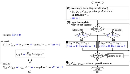
Figure 9.
(a) Correlation among different parameters for (b) flow chart of proposed calibration process.
Based on (7) and Figure 9a, the flow chart for this work is described as shown in Figure 9b. The process in the flow chart is performed to calibrate capacitances, i.e., the second step of the proposed work. All those procedures are controlled by the linear search engine in cal unit shown in Figure 3c. Initially, right after the precharge step is completed. We put numbers from #1 to #8 for each flow of Figure 9b. In #1, in (7) is measured by comp1, and then if comp1 output or case1 (i.e., and ), then it is also asked if the current in #2 to see if we were previously in case2, or to see if we are in the transition between cases 1 and 2. Because initially , we go to #4, and becomes 1 to represent the case1. In addition, is decreased by a step size of a MOSCAP, thereby updating . Then, we go back to #1 to check if comp1 output after is measured again, because has a correlation with the updated , as shown in (7). If comp1 output in this time, then we go to #3, which is case2. Because we were previously in case1 and thus currently , this moment is the transition from case1 to case2, which can be considered as the moment when or , and thus, the linear search finishes for the calibration of , as discussed earlier. may be correlated with its parasitic capacitances, and as shown in (7), and thus , which exhibits the correlation in (7), is identified to meet for the calibration of . Next, we go to #6 to check if cal.seq (i.e., the last calibration sequence of Table 2). If not, then the second calibration sequence is set in #7 (i.e., cal. seq. ), which is discussed further below.
There can be a trade-off between and the process time of the linear search, as in a general linear search method; the higher the value of , the sooner the linear search can be performed, and the less accurate the searched value (or vice versa). In addition, the following relation can be concluded from (7) to meet :
The second calibration sequence of Table 2 calibrates using a sum of and , which has been previously calibrated, and thus can be reused as a reference capacitor, as shown in Figure 10. Similarly, is open. and of ADC1 and of ADC2 are connected in antiparallel to the top and bottom plates, by setting on , and by setting and on and , respectively, as shown in Figure 10a,b. is connected to (omitted for simplicity), as in Figure 7b. All other capacitors are disconnected from the top and bottom plates; in addition, comp2 is disabled while comp1 is enabled. As a result, is connected to and in antiparallel, as depicted in Figure 10c.
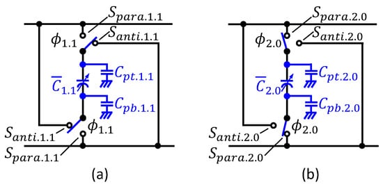
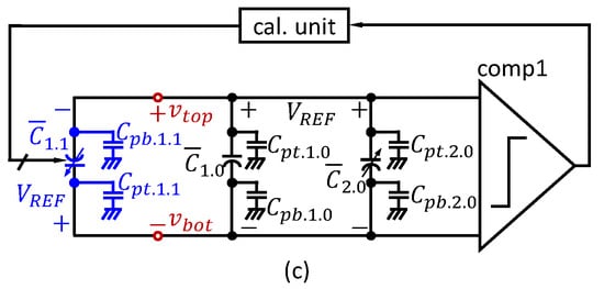
Figure 10.
Connections for para-switches of (a) and (b) to go into (c) calibration mode in antiparallel connection, along with .
in Figure 10c is obtained based on the charge conservation, as follows. When , , and are initially connected in antiparallel, is still dropped across each capacitor immediately after the precharge step. As shown in Figure 10a–c, and are similarly modeled as the parasitic capacitances on the top and bottom plates of and , respectively. Then, the overall initial charge and on the top and bottom plates in antiparallel circuit in Figure 10c can be identified as
where , , and . In addition, , , and . and are the initial charges on the top and bottom plates of , respectively, which are made in the precharge step.
On the other hand, if , then the overall final charge and on the top and bottom plates can be found as
Then, the two relations, and are obtained by the charge conservation, and those can be described using (9) and (10), as follows:
where , , , and . Finally, is obtained by solving the simultaneous equations of (11) as
As in the previous example, the linear search engine in cal unit finds that satisfies in (12). The flow chart of Figure 9b works for this example as well. may be correlated with its parasitic capacitances as shown in (12), and thus is identified to also meet for the calibration of . In addition, the following relation can be concluded from (12) to meet .
All other calibration sequences in Table 2 can be also similarly processed. It can be observed in Table 2 that one (or two) reference capacitor is used in the odd (or even)-numbered calibration sequence. In summary, the proposed calibration scheme updates all the capacitances to be in the binary-weighted relation using only one or two reference capacitors, based on an actually fabricated LSB capacitor , instead of forcedly updating each capacitance into a specific value predefined by the design specifications. In addition, the proposed method is inherently conducted upon every power up, as in all other foreground calibration methods.
In general, the capacitor mismatch of a CDAC in SAR ADCs degrades the signal-to-noise ratio (SNR) results, leading to a decrease in the effective number of bits (ENOBs) [17]. As discussed earlier, the voltage generation circuit is used to find an accurate for the linear search. required by the linear search is applied to each MOSCAP to be set to a correct capacitance. As a result, the capacitor mismatch should be significantly mitigated, resulting in a higher SNR or ENOBs, which can be the best achievable resolution of the ADC.
The application areas most suitably applied by this work can be considered as three specifications of ADCs. The SAR ADC, the pipelined ADC, the two-step ADC, and the subranging ADC, for which a CDAC can be applied, are suitable architectures, because this work calibrates the CDAC. The high-resolution ADCs are also proper, since those further require the calibration, compared to lower-resolution ADCs. The sampling rates from about 1MSPS to tens of MSPS are suitable, because those can be determined by the above two conditions based on the trend of ADCs [18].
Several benefits of this work are summarized as follows:
- The proposed work does not require an adaptive algorithm, e.g., LMS as in [10], and thus, the heavy calculation process is not needed, and a digital hardware logic for calculation, i.e., a calibration unit, can be much simpler.
- This work does not require a dummy unit capacitor, e.g., , by employing a two-ADC channel configuration. In [14], is required to make the number of capacitors a power of 2, so that under calibration can be compared with by a comparator for the capacitor mismatch calibration. For the proposed work, two unit capacitors are available from the two original ADC channels, and thus those capacitors facilitate the capacitance calculation based on a power of 2 without a dummy unit capacitor, as shown in Table 2.
- Using a small number (i.e., at most two) of the reference capacitors allows this work to make simple connections between capacitors as well as simple calculations in cal unit. For example, in [14], which used a 16-bit ADC, is calibrated using one reference comparator, . is calibrated using two reference capacitors, ; and finally, calibrating requires a sum of 16 reference capacitors, . Thus, a total of 136 reference capacitors are required to calibrate all the 16 capacitors of the CDAC. Ultimately, an N-bit ADC is calibrated using exponentially increased reference capacitors. On the other hand, the proposed work with a 16-bit ADC uses only 46 reference capacitors to calibrate all the capacitors of the two ADC channels. Thus, an N-bit ADC is calibrated using linearly increased reference capacitors for this work. As a result, this work uses only , and of the reference capacitors required for [14] (i.e., ), for , and 18-bit ADCs, respectively. Therefore, as an ADC has higher resolution, i.e., more capacitors, the proposed calibration scheme significantly reduces the complexity both in the connection of the capacitors and the calculation process in cal unit.
Considering the limitation of this work, the proposed work requires the design efforts for the proposed calibration unit integrating the voltage generator and the linear search engine. In addition, it is not easy to calibrate the calibration unit itself on a device-by-device basis, as most on-chip calibration methods inherently suffer from the same issue.
3.3. Nonidealities
3.3.1. Energy
The energy consumption is discussed for the proposed work, in terms of two different phases: the calibration phase and the normal operation phase. The proposed calibration method is assumed to be conducted in the fabrication process, because it is a foreground calibration.
Firstly, the energy for the precharge step of the calibration phase is primarily consumed by charging the MOSCAPs of the CDAC shown in Figure 5, as in a conventional CS-SAR ADC. for ADC1 can be considered as
where is a sum of the charges on all the MOSCAPs during the precharge step, and is that in the previous status (i.e., no connection of the MOSCAPs, before the start of the precharge). Thus, of the split ADC can be
As discussed in Section 2.2, the total capacitance of the two ADC channels in a split ADC is identical to that of a conventional ADC. Thus, it is concluded from (15) that the energy consumption of this work based on the split ADC is the same as that of a conventional ADC as well. All other circuits such as the comparators and cal unit are inactive in the precharge step.
Then, the energy consumption for the calibration step of the calibration phase is considered. For a conventional CS-SAR ADC, the CDAC passively operates after the precharge step, contrary to the CR-SAR ADC. In addition, the comparator inputs have infinite impedance, and so no current is drained out of the CDAC [16]. Therefore, there is no primary energy consumed by the MOSCAPs for the CDAC of the proposed calibration, even though the charges are moved among different MOSCAPs by varying capacitance. For the voltage generator employed from [14], it is implemented mainly using three capacitors (i.e., , , and ), and thus, the energy consumption can be calculated as , where is a reference source voltage for the generator, and the number 15 means the total number of calibration sequence as discussed for Table 2.
Secondly, the energy consumption for the normal operation with the calibrated MOSCAPs can be as follows. The energy for the precharge of the normal operation phase should be identical to that in the discussion for (15). The primary energy for the CDAC in the binary search step of conventional SAR ADC is not consumed by the MOSCAPs with the calibrated capacitance, because the CDAC still behaves passively, as discussed earlier. For the voltage generators, is disconnected from the generator after completing the calibration process, and the charges from for the already calibrated capacitors are held in each of , , and . Thus, there is no energy consumption by the generator in the normal operation.
3.3.2. Area
Next, the chip area can be discussed as follows. In general, the overall chip area of a conventional SAR ADC is limited by the area of the CDAC, which consists of binary-weighted capacitors. Capacitors take up most of the area of a conventional SAR ADC, and thus the chip area is determined by the capacitance density [19,20]. The area of the CDAC is thus used to estimate the chip area of this work, even though our future efforts will incorporate the silicon implementation of this work. This is an example of the area estimations, assuming the conservative unit capacitance of and the capacitance density of m2 [21], based on a 130 nm process, although a practical unit capacitor has a much lower value than this. Because each ADC channel of a split ADC has half of the capacitance compared to that of a conventional ADC, a unit capacitor can be assumed to be . The total capacitance of ADC1 is , and that of a split ADC would be . Therefore, the total area of the CDAC for this work can be estimated as m2.
3.3.3. Noise
Here, we discuss the noise. Firstly, the noise in the proposed calibration mode can be analyzed as follows. For the precharge step, the thermal noise charge caused by the precharge switches in the CDAC is
where . For the capacitance calibration step, the thermal noise charge introduced by the para-switches of all the capacitors that participated in the corresponding calibration sequence is
where represents a sum of the reference capacitance(s) and the capacitance under calibration described in Table 2, e.g., for the second calibration sequence. Considering the comparator noise, the total capacitance of the CDAC increases during the linear search process for each calibration sequence. From the comparator point of view, decreases, and the SNR is lower, assuming a fixed value of noise. Basically, the effect of the comparator noise may change depending on the combination of the capacitors in the CDAC. It is not trivial to model the comparator noise for the proposed calibration, and thus its derivation is out of the scope for this work. However, the simulation results in Section 4.1 addressed the effect of the comparator noise.
Secondly, the noise analysis for the normal operation mode can be discussed as follows. The thermal noise in the precharge step is identical to that of the calibration mode. For the sampling step, the thermal noise charges caused by the para-switches of each capacitor used for each bit-decision cycle are
where and are the noise charges occurring in the CDACs of ADC1 and ADC2, respectively. and are the capacitance sum of the capacitors participated during the sampling process for each bit-decision cycle in ADC1 and ADC2, respectively. As in the proposed calibration mode, the effect of the comparator noise may change depending on the combination of the capacitors in the CDAC, and thus, it was included in the simulation results.
4. Experimental Results and Discussion
The behavioral simulations were performed to validate the performance of the proposed calibration scheme using MATLAB. Two 8-bit CS-SAR ADCs were modeled to configure a conventional split ADC. This work itself is not limited to an 8-bit-resolution ADC, and the proposed work can be simply applied to higher-resolution ADCs. The example of an 8-bit ADC in this paper (Section 3 and Section 4) is used to discuss this work in a consistent manner and to provide a simpler explanation. For the proposed calibration configuration, the capacitor array for the CDAC was modeled with a nonlinear MOSCAP, and the proposed calibration unit was built. The MOSCAPs used in the simulation were assumed to have of the average capacitances as their capacitance ranges, and their linear ranges were carefully used for the simulation. Capacitance mismatches were set from to , and the standard variation of each capacitance was 1% as in typical capacitors. In addition, Gaussian random noises were set in the circuits for practical conditions.
4.1. Results of Proposed Calibration Scheme
The proposed calibration process was performed from the LSB capacitors to the MSB capacitors, and then the critical performances of the ADCs were measured before and after applying this work, as shown in Figure 11, Table 4, Figure 12, and Table 5. The legend before calibration in all the plots and tables in Section 4.1 indicates the results measured from a conventional (single-channel) CS-SAR ADC, which was not calibrated. On the other hand, the legend after calibration represents the results obtained based on this work. The identical capacitor mismatches were applied to the ADCs used to obtain each of those two results indicated by the legends before calibration and after calibration. It should be noted that the result comparison between a conventional split ADC and this work is discussed in Section 4.2.
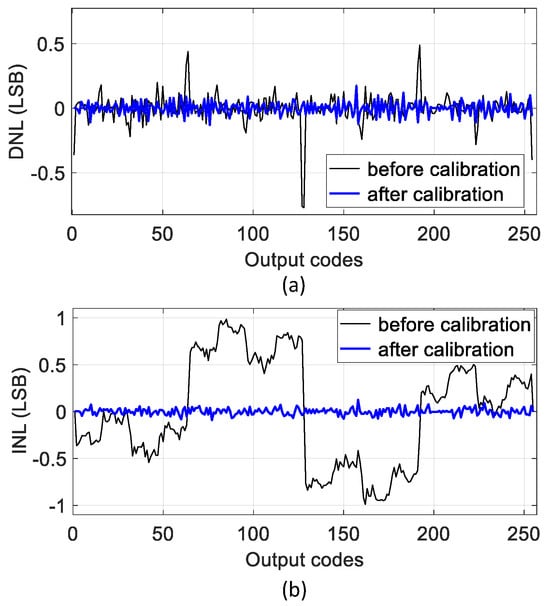
Figure 11.
(a) DNL and (b) INL plots measured before and after applying this work.
Table 4.
DNL and INL results acquired before and after applying this work.
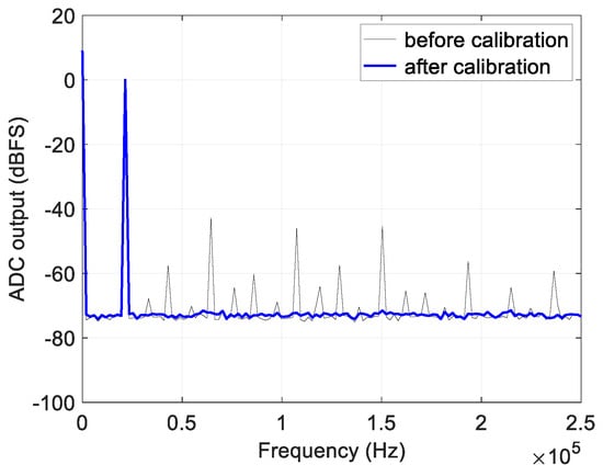
Figure 12.
Spectral responses obtained before and after applying this work.
Table 5.
Dynamic performances acquired before and after applying this work.
To evaluate the static performance of ADCs calibrated by this work, a conventional histogram-based differential nonlinearity (DNL) and integral nonlinearity (INL) method [22] was conducted by applying a ramp signal to both of a single CS SAR ADC (for before calibration) and a split ADC with the proposed calibration (for after calibration). The outputs of each ADC were then captured to obtain the code widths translated into the histogram results. Their DNL and INL results were acquired as shown in Figure 11, and Table 4 summarizes the results. Both DNL and INL results of before calibration were quite poor, compared to those of after calibration. In particular, because the mismatches of the MSB and the MSB capacitors heavily affect the overall performance of an ADC in general, a couple of high peaks can be observed around the MSB and the MSB codes in the DNL plot, e.g., a center code, and more. Accordingly, abrupt changes are observed in those output codes of the INL plot.
A conventional DSP-based test using the coherence sampling [22] was performed to accurately measure the dynamic performances of the ADC calibrated by the proposed scheme. A kHz single-tone sinusoidal signal was applied to both a single ADC (for before calibration) and a split ADC based on this work (for after calibration). The stimulus was set to dBFS in order to avoid any clipping of their output signal, as in conventional production testing. A total of samples were captured by each ADC at 1-MSPS. The spectral responses of each ADC are shown in Figure 12, and the dynamic performance parameters are summarized in Table 5. In addition, the harmonic coefficients up to the 10th order [23] were used to obtain the total harmonic distortion (THD) results. It is clear that SNR, THD, and signal-to-noise-and-distortion ratio (SINAD) were significantly enhanced by the proposed calibration scheme. Thus, this work can be practically used as a foreground self-calibration solution for SAR ADCs.
4.2. Comparison with Conventional Split ADC
As previously discussed in Section 2, the aim of this work is to overcome the issue of a conventional split SAR ADC [10], which exhibits low calibration accuracy if two ADC channels have similar mismatches to be similar outputs. To validate the performance of this work, an identical set of the capacitor mismatches from 4 to 8% was applied to the same bit level of capacitors in the two channels of a split ADC, so that both the ADC channels can exhibit similar errors, e.g., the same 8% of the capacitor mismatch on both and . Under this condition, each of the split ADCs [10] and this work completed their calibration processes. The results are shown in Table 6. All the performances were significantly improved by this work. In addition, the performance of this work was evaluated, even in the case that both ADC channels showed different errors, and the results are shown in Table 7. It was validated that SNR, THD, and SINAD of a split ADC calibrated by this work were compatible with those of a conventional split ADC [10], if both the ADCs have different errors.
Table 6.
Calibration performance comparison between a conventional split ADC and this work, in the case of two channels showing similar errors.
Table 7.
Calibration performance comparison between a conventional split ADC and this work, in the case of two channels showing different errors.
4.3. Nonidealities for Calibration
The effects of nonideality can be considered to analyze the calibration performance of the proposed work in practical situations. This section evaluates the performance of this work by different levels of capacitor mismatch, and by the number of the conversions.
4.3.1. Levels of Capacitor Mismatch
As discussed previously, the dynamic performances of SAR ADCs are limited by the capacitor mismatch, and different levels of the mismatch can be introduced by the variations of the practical manufacturing process. Because the mismatch on the MSB capacitance seriously affects the CDAC performance, the SNR, THD, and SINAD of an ADC calibrated by the proposed work were analyzed by increasing the mismatches on the MSB capacitors up to 13% in the simulation. As the mismatch increased, each of the SNR, THD, and SINAD almost exponentially diminished before applying this work, while those obtained after applying the proposed work were overall consistent, as shown in Figure 13. Because of capacitive variation present in the variable capacitors, the performances by the proposed work exhibited small variations.
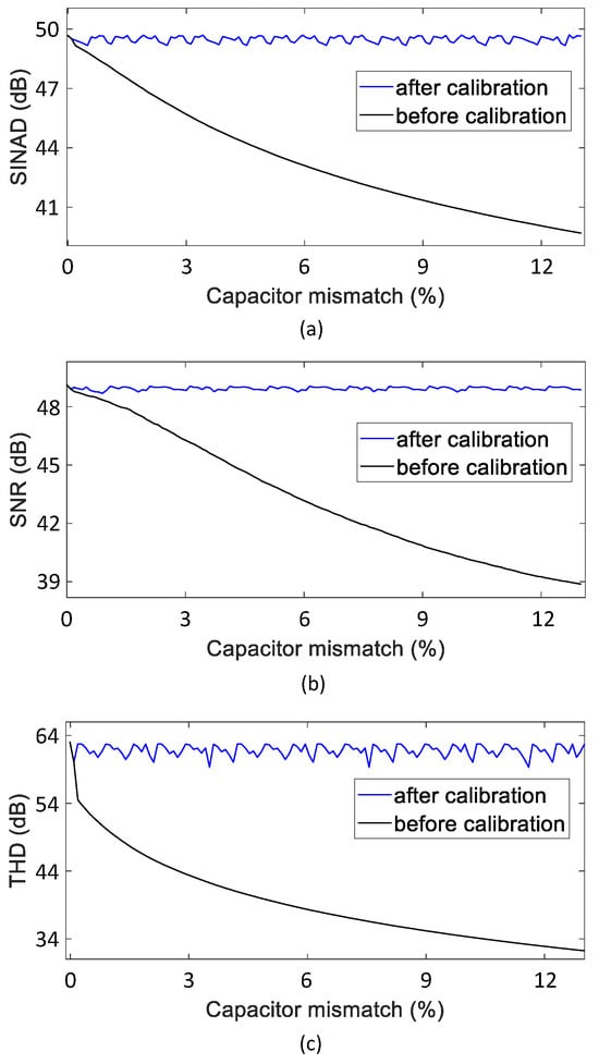
Figure 13.
(a) SINAD, (b) SNR, and (c) THD as a function of capacitor mismatch on MSB capacitor.
4.3.2. Number of Conversions
The linear search process is performed to update each capacitor under calibration by monitoring the outputs of comp1 for this work, as discussed in Section 3. Figure 14 shows how the SNR and THD of a split ADC were improved, as the capacitors were calibrated from the LSB to the MSB capacitors in the calibration. Overall, as the conversion went on, SNR and THD were enhanced. The total number of conversions was 2364. In particular, because the proposed calibration is processed from the LSB to the MSB capacitor, both of SNR and THD rose steeply from the conversion index 1861, at which the proposed calibration for the MSB-1 capacitor was completed.
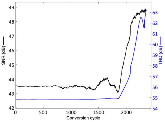
Figure 14.
Performances as a function of conversions.
5. Conclusions and Future Work
This paper proposed a promising foreground self-calibration scheme that improves the linearity of the SAR ADCs by significantly alleviating the capacitor mismatches efficiently using the split ADC architecture along with variable capacitors. In this work, two CS-SAR ADC channels of the split ADC have their CDACs whose binary-weighted capacitors are implemented using variable capacitors. In the normal operation mode, their digital outputs are averaged to be the final ADC output. For the calibration mode, every single binary-weighted capacitor of a split ADC is calibrated one at a time. For instance, of ADC1 can be updated to be closest to the sum of of ADC1 and of ADC2 by comparing those two capacitances using comp1 based on the reconfiguration. The comparison process can be iterated by updating with the linear search, till is in agreement with the sum of two of . Finally, all the capacitors can be calibrated in this way to have the binary-weighted relation. The simulation results based on the proposed work with an 8-bit split SAR ADC model verified that the proposed scheme can be practically used, by showing that THD and SINAD were enhanced by dB and dB, respectively. Therefore, this work efficiently overcomes the limitation of the calibration accuracy of the conventional split SAR ADC, in the case that the similar capacitor mismatches are present in both ADC channels. Our future efforts will incorporate the hardware measurements with a fabricated chip (i.e., a 12-bit SAR ADC integrating the calibration circuits with 11 layers in 28 nm CMOS) to verify the performances of this work more practically, which can be affected by the nonideal components. Our extended work will be reported with the hardware measurement results mentioned above.
Author Contributions
Conceptualization, J.P. and B.K.; methodology, J.P. and B.K.; data curation, J.P. and J.L.; simulation J.P. and J.L.; writing and original draft preparation, J.P. and B.K.; review and editing, J.A.A.; supervision, B.K. All authors have read and agreed to the published version of the manuscript.
Funding
This research was supported in part by Basic Science Research Program through the National Research Foundation of Korea (NRF) funded by the Ministry of Education (No. 2016R1D1A1B020 13884). This research was also supported in part by Korea Institute for Advancement of Technology (KIAT) grant funded by the Korea Government (MOTIE) (P0012451, The Competency Development Program for Industry Specialist). This research was also supported in part by the MOTIE (Ministry of Trade, Industry and Energy) (1415180306) and KSRC (Korea Semiconductor Research Consortium) (20019164) support program for the development of the future semiconductor device, and the research fund of Hanyang University (HY-2017-N).
Data Availability Statement
Data available on request due to privacy.
Acknowledgments
The EDA tool was supported by the IC Design Education Center (IDEC), Korea.
Conflicts of Interest
The authors declare no conflicts of interest.
References
- Kilani, D.; Mohammad, B.; Alhawari, M.; Saleh, H.; Ismail, M. Power Management for Wearable Electronic Devices; Springer: Berlin/Heidelberg, Germany, 2020. [Google Scholar]
- Hermann, B. Enhancing Battery Life and Audio Performance in Mobile Devices; Maxim Integrated Corp.: San Jose, CA, USA, 2018. [Google Scholar]
- Pasricha, S.; Ayoub, R.; Kishinevsky, M.; Mandal, S.K.; Ogras, U.Y. A Survey on Energy Management for Mobile and IoT Devices. IEEE Des. Test 2020, 37, 7–24. [Google Scholar] [CrossRef]
- O’Driscoll, S.; Shenoy, K.V.; Meng, T.H. Adaptive Resolution ADC Array for An Implantable Neural Sensor. IEEE Trans. Biomed. Circuits Syst. 2011, 5, 120–130. [Google Scholar] [CrossRef][Green Version]
- Maxim. Understanding SAR ADCs: Their Architecture and Comparison with Other ADCs. In Tutorials 1080; Maxim Integrated Corp.: San Jose, CA, USA, 2001. [Google Scholar]
- Mueller, J.H.; Strache, S.; Busch, L.; Wunderlich, R.; Heinen, S. The Impact of Noise and Mismatch on SAR ADCs and a Calibratable Capacitance Array Based Approach for High Resolutions. Int. J. Electron. Telecommun. 2013, 59, 161–167. [Google Scholar] [CrossRef]
- Chang, A.H.T. Low-Power High-Performance Sar ADC with Redundancy and Digital Background Calibration. Ph.D. Thesis, Massachusetts Institute of Technology, Cambridge, MA, USA, 2013. [Google Scholar]
- Youn, E.; Jang, Y. 12-bit 20M-S/s SAR ADC Using C-R DAC and Capacitor Calibration. In Proceedings of the International SoC Design Conference, Daegu, Republic of Korea, 12–15 November 2018; pp. 1–2. [Google Scholar]
- Salib, A.; Flanagan, M.F.; Cardiff, B. A Generic Foreground Calibration Algorithm for ADCs with Nonlinear Impairments. In Proceedings of the International Symposium on Circuits and Systems (ISCAS), Florence, Italy, 27–30 May 2018; pp. 1–4. [Google Scholar]
- McNeill, J.; Coln, M.; Larivee, B. “Split ADC” Architecture for Deterministic Digital Background Calibration of A 16-bit 1-MS/s ADC. IEEE J. Solid-State Circuits 2005, 40, 2437–2445. [Google Scholar] [CrossRef]
- Pena-Ramos, J.C.; Verhelst, M. Split-Delta Background Calibration for SAR ADCs. IEEE Trans. Circuits Syst. II Express Briefs 2017, 64, 221–225. [Google Scholar] [CrossRef]
- Bagheri, M.; Schembari, F.; Pourmousavian, N.; Zare-Hoseini, H.; Hasko, D.; Staszewski, R.B. A Mismatch Calibration Technique for SAR ADCs Based on Deterministic Self-Calibration and Stochastic Quantization. IEEE Trans. Circuits Syst. I Regul. Pap. 2020, 67, 2883–2896. [Google Scholar] [CrossRef]
- McNeill, J.A.; Chan, K.Y.; Coln, M.C.W.; David, C.L.; Brenneman, C. All-Digital Background Calibration of a Successive Approximation ADC Using the ”Split ADC" Architecture. IEEE Trans. Circuits Syst. I Regul. Pap. 2011, 58, 2355–2365. [Google Scholar] [CrossRef]
- Rabuske, T.; Fernandes, J. A 12-Bit Sar ADC with Background Self-Calibration Based on A MOSCAP-DAC with Dynamic Body-Biasing. In Proceedings of the International Symposium on Circuits and Systems (ISCAS), Montreal, QC, Canada, 22–25 May 2016; pp. 1482–1485. [Google Scholar]
- Craninckx, J.; van der Plas, G. A 65fJ/conversion-step 0-to-50MS/s 0-to-0.7mW 9b charge-sharing SAR ADC in 90nm digital CMOS. In Proceedings of the International Solid-State Circuits Conference (ISSCC), San Francisco, CA, USA, 11–15 February 2007; pp. 246–600. [Google Scholar]
- Rabuske, T.; Fernandes, J. Charge-Sharing SAR ADCs for Low-Voltage Low-Power Applications; Springer: Berlin/Heidelberg, Germany, 2017. [Google Scholar]
- EDN. ADC SNR Effects Due to Parasitics, Mismatch, and Noise. 2015. Available online: https://www.edn.com/adc-snr-effects-due-to-parasitics-mismatch-and-noise (accessed on 1 February 2024).
- Kester, W. Which ADC Architecture Is Right for Your Application? ADI Analog Dialogue 2005. Available online: https://www.analog.com/en/resources/analog-dialogue/articles/the-right-adc-architecture.html (accessed on 1 February 2024).
- Zhu, X.; Chen, Y.; Tsukamoto, S.; Kuroda, T. A 9-bit 100MS/s tri-level charge redistribution SAR ADC with asymmetric CDAC array. In Proceedings of the Technical Program of 2012 VLSI Design, Automation and Test, Hsinchu, Taiwan, 23–25 April 2012; pp. 1–4. [Google Scholar]
- Yoshioka, K.E.A. A 20ch TDC/ADC hybrid SoC for 240X96-pixel 10%-reflection > 0.125%-precision 200m-range imaging LiDAR with smart accumulation technique. In Proceedings of the International Solid-State Circuits Conference (ISSCC), San Francisco, CA, USA, 11–15 February 2018; pp. 92–94. [Google Scholar]
- Rabuske, T.; Fernandes, J. A SAR ADC with a MOSCAP-DAC. IEEE J. Solid-State Circuits 2016, 51, 1410–1422. [Google Scholar] [CrossRef]
- Burns, M.; Roberts, G.W. An Introduction to Mixed-Signal IC Test and Measurement; Oxford Univeristy Press: New York, NY, USA, 2001. [Google Scholar]
- IEEE Std 1241-2010; Standard for Terminology and Test Methods for Analog-to-Digital Converters. IEEE: New York, NY, USA, 2011.


Disclaimer/Publisher’s Note: The statements, opinions and data contained in all publications are solely those of the individual author(s) and contributor(s) and not of MDPI and/or the editor(s). MDPI and/or the editor(s) disclaim responsibility for any injury to people or property resulting from any ideas, methods, instructions or products referred to in the content. |
© 2024 by the authors. Licensee MDPI, Basel, Switzerland. This article is an open access article distributed under the terms and conditions of the Creative Commons Attribution (CC BY) license (https://creativecommons.org/licenses/by/4.0/).