Abstract
The ambipolar conduction property of graphene field-effect transistors (GFETs) and the inherent square-like dependence of the drain current on the gate voltage, enable the development of single-device architectures for analog nonlinear radiofrequency (RF) circuits. The use of GFETs in novel RF component topologies allows leveraging graphene’s attractive thermal and mechanical properties to improve the miniaturization and weight reduction of electronic components. These features are specifically appealing for integrated sensing, modulation, and transmission systems. However, given the innovative nature of emerging graphene-based technology, a complete performance analysis of any novel electronic component is essential for customizing the operating conditions accordingly. This paper presents a comprehensive circuital analysis of a GFET-based frequency doubler, exploiting a compact model for GFET circuit simulation to assess the device’s performance parameters, including power conversion gain bandwidth and saturation. The performed analysis proposes to support the design of GFET-based harmonic transponders, offering integrated sensing and signal manipulation capabilities.
1. Introduction
Frequency multiplication is a common operation performed by nonlinear electronic circuits for a wide plethora of applications. Shifting the frequency of a reference signal is generally easier than generating a signal at an arbitrary frequency, and allows relaxing the complexity of other parts of the electronics for the signal manipulation, allowing the design of more performing circuits under less demanding requirements. The frequency up conversion therefore enables the development of electronic circuits capable of enhancing either data transmission capacity and rate, or spatial resolution, miniaturization, power consumption, based on the considered application. In general, frequency multipliers are relevant for any improvement related to the increase of the system’s operating frequency. Hence, research in novel devices and architectures for frequency multiplication is powered by the interest in opening new possibilities for applications in the sub-THz and THz frequency range [1].
The key application of electronic circuits performing frequency multiplication has historically been that of signal modulation and mixing for wireless communication systems. However, frequency multipliers are also a basic component of test and measurement equipment, such as spectrum analyzers, and medical imaging equipment, such as magnetic resonance and ultrasound devices.
Traditional Silicon-based frequency multiplier circuits include diode-based multipliers (varistor or varactor type), known for wideband and low-noise operation, and active transistor-based multipliers, with higher conversion gain but increased noise. In these two cases, the generation of higher harmonics is obtained either by clipping the output waveform or by exploiting the nonlinearity of the input-output relation. Concerning nonlinear analog circuits for high-frequency RF applications, graphene has shown great potential among the emerging technologies [2]. The peculiar capability of tuning the polarity of charge carriers across the channel of a graphene field-effect transistor (GFET) by simply acting on the gate bias inspires the development of single-device ambipolar circuits that are usually made of several transistors, with the consequent area, mass, and power saving, which are crucial for several critical applications [3]. Circuits that typically exploit the ambipolar conduction and the nonlinear relation between the drain voltage and the gate voltage of GFETs are mixers, phase shifters, frequency multipliers.
The first experimental demonstration of a GFET-based frequency doubler dates back to 2009 [4], when a 10 kHz sine waveform was multiplied by a single back-gated GFET obtaining >90% RF power delivered to the second harmonic. Shortly after, an improved GFET with a top-gate design allowed better performance providing frequency multiplication from 100 kHz to 200 kHz [5], and then from 700 MHz to 1.4 GHz, achieving a spectral purity >90% [6] against the ~35% obtained from traditional unipolar field-effect devices. Following, the progress in the RF-GFET transistor fabrication allowed achieving the first above-cut-off 3-GHz frequency doubler [7], and the first single-transistor frequency doubler operating in the Ku-band, up to 16 GHz [8]. From that moment, inspired by the impressive results obtained for the frequency doublers, GFETs were proposed also for the design of frequency triplers [9] and quadruplers [10] by exploiting a W-shaped drain current-gate voltage transfer curve, achieved by using two GFETs in series and a double-gate GFET configuration, respectively. Overall, the GFET-based frequency multipliers have outperformed other transistor technologies [11]. However, technological limitations are still hindering the widespread diffusion of graphene-based electronic devices, due to the issues related to graphene deposition and transfer process and non-negligible sensitivity to manufacturing-related uncertainties [12]. These issues hold graphene-based components from achieving the high-frequency performance of state-of-the-art traditional silicon electronics and III-V compound semiconductor technology. Both technologies can deliver gain up to frequencies above 100 GHz, making them readily applicable to cutting-edge high-frequency RF wireless communications. Nevertheless, the interest towards graphene electronic devices lies in their versatility, allowing multiple applications to be integrated into a single component, rather than on achieving top-level performance.
Besides the interesting opportunities in RF electronics, GFETs have gained great attention mostly as high-sensitivity chemical sensors and biosensors [13,14,15]. Thanks to the successful demonstration of single-molecule high-sensitivity sensing property, and being the simplest device capable of delivering high-purity frequency multiplication (especially at double-frequency harmonic component), the GFET was considered for the realization of nanomaterial-based harmonic transponders [16,17]. In this application, the GFET acts as a chemically-sensitive frequency multiplier: the chemical gating effect causes a shift of the transistor’s Dirac point, thus modulating the second-harmonic output signal and affecting the nonlinear conversion gain. Based on the fact that graphene can also be employed for energy harvesting applications and for tunable high-frequency antennas, it is possible to envisage all-graphene systems for combined sensing, modulation, and transmission, with the added value of being light-weight, small-footprint, low-power, in line with the ongoing Internet of Things and forthcoming Internet of Everything scenario. This envisaged application takes advantage of the unique characteristics of GFETs, offering the potential to integrate the functionality of sensing and modulation within a single component. Due to the frequency limitation and the fabrication-related performance impairment, at the present stage of technological implementations, graphene technology can be explored to develop integrated systems working below the sub-THz frequency range. The advantage related to the shift towards this novel technology remains in the development of lightweight, small, thermally-efficient, power-saving components. On the other hand, as nanotechnology is still in the first stages, the absence of established design rules poses a significant challenge for designers seeking to define optimal operating conditions and selection criteria during the system parameter setup. To address this challenge, this work proposes an original analysis of the performance of a GFET-based frequency doubler model, providing choice criteria for making informed decisions during the design of operating conditions of GFET-based signal modulators. Building on our previous activity [3,12,18] and exploiting a GFET Verilog-A model of proven reliability, the proposed work explores the application of a recently presented high-performing GFET [19] to the frequency doubling operation by carrying out circuit simulations. The analysis is approached by comprehensively computing relevant figures of merit under varying conditions, such as different bias points and operating frequencies. In this way, the proposed study targets the definition of criteria not yet available in the literature for the design of the intrinsic GFET operating conditions. Therefore, it supports the simulation-based design of novel components bypassing the need for expensive prototypes and time-consuming measurements.
In this paper, the operational principle of a single-device frequency doubler based on an intrinsic (i.e., without any external component) graphene field-effect transistor device is described in Section 2, discussing the relevance of the bias point for the frequency multiplication. In Section 3, the simulated GFET device is described, and the model validity is verified by comparing the simulation results with available measurement data. The frequency doubler’s performance in the frequency domain and its dependence on the input power level is explored in Section 4, by evaluating relevant figures of merit such as the power conversion gain and the output power delivered at doubled frequency. The presented results are discussed in Section 5, drawing some considerations on the application of GFETs in combined sensing and modulation applications. Finally, the conclusions are reported in Section 6.
2. Operational Principle of a Single-Device GFET-Based Frequency Doubler
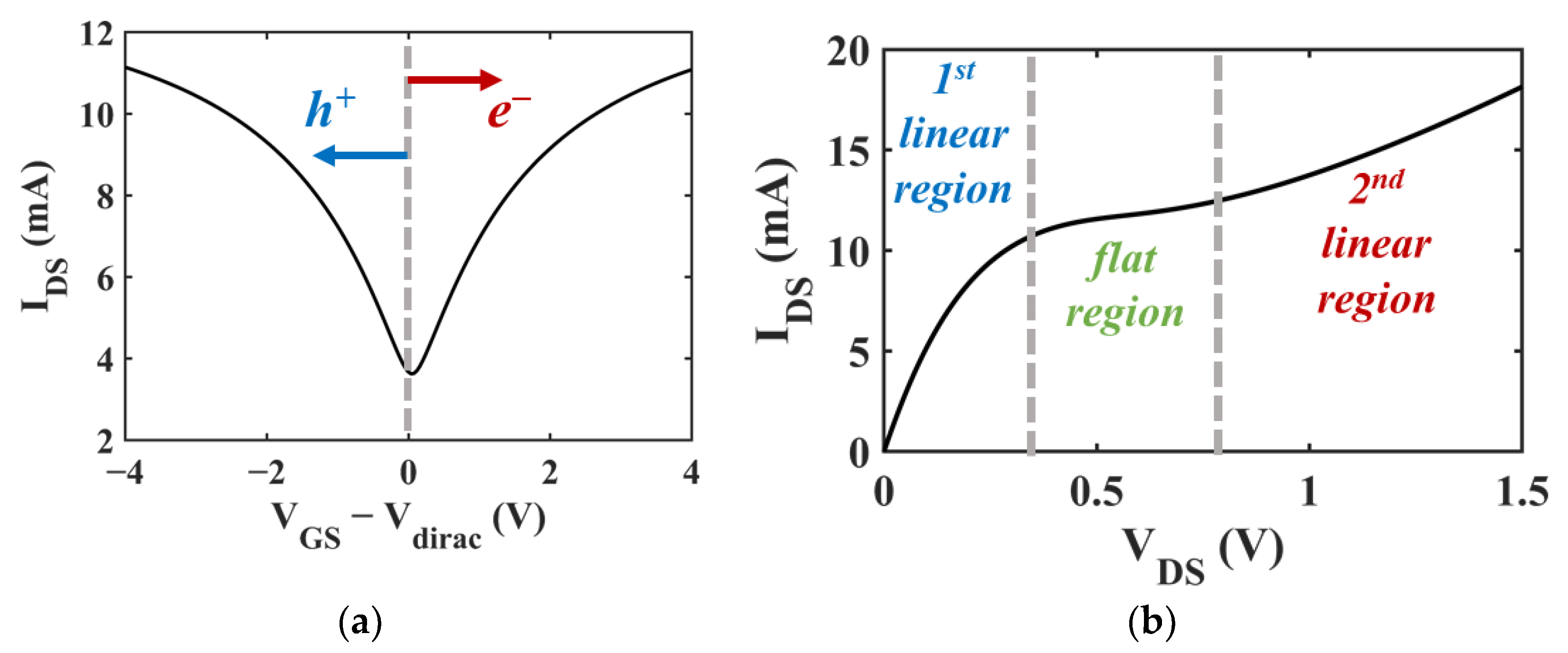
The ambipolar conduction of charge carriers across the graphene channel is a consequence of the V-shaped transfer curve of GFETs, which enables changing the polarity of the current, ID, by varying the gate-source voltage, VGS. The polarity of the drain-source current (IDS) switches from p-type to n-type when the gate-source bias VGS crosses the minimum conduction point (Dirac point), generally referred to as the Dirac voltage, Vdirac. Figure 1a reports the IDS-VGS transfer curve of a typical GFET simulated by a compact model for DC operation. In Figure 1a, the transfer curve is symmetrical because the model adopted for the circuit simulation assumes that, as in [20], the mobility of both holes and electrons is the same, and the saturation velocity is independent on the carrier density. Under these assumptions, the value of Vdirac is roughly given by Vdirac = VG0 + (VD + VS)/2 [21], where VG0 is the gate voltage offset due to charges trapped in the graphene channel, and VD and VS are the voltage values at the drain and source terminal, respectively.

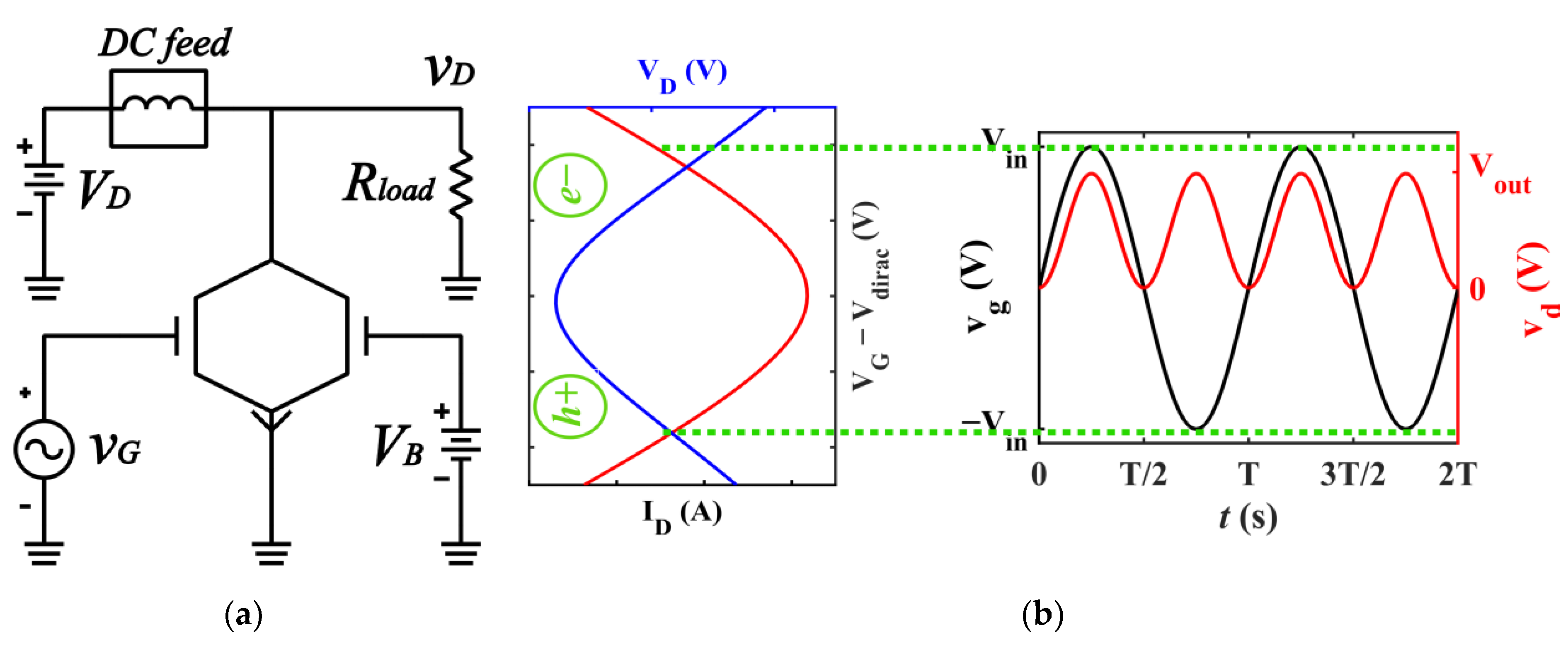
Figure 1.
(a) Simulated transfer curve of a generic GFET. The left branch before the minimum conductivity point (VGS = Vdirac) corresponds to a p-type charge transport; the right branch corresponds to an n-type charge transport. Operating the GFET around the Vdirac allows doubling the frequency of the gate signal at the device drain terminal. (b) Simulated static I/O curve of a generic GFET. The static characteristic of this device shows a flat region in the VDS range corresponding to the minimum charge density point entering the channel, determining the charge polarity inversion in the channel. The first linear region of the curve is related to hole conduction, and the second to electron conduction.
The static gate and drain bias point (VGS, VDS) is fundamental for the correct operation of the frequency doubler: it is important that, at the chosen operating point, the small-signal variation of the drain current depends on the square of the gate voltage while being linearly dependent upon the drain voltage [22]. When the transistor is biased at the Dirac point and a drain voltage is applied, both types of carriers are injected in the channel and recombine. This condition is represented in Figure 1b by the region in proximity of VDS = 0.5 V. For this reason, even by increasing the VDS, the IDS does not increase, and the current curve shows the typical inflection point related to the carrier polarity inversion [23,24]. If biased in this flat region, in which the odd symmetry property is lost, odd harmonics of the input signal can appear in the output waveform, impairing the output voltage spectral purity and reducing the power transfer to the harmonic of interest [22], that, in the case of the frequency doubler, is the first even harmonic component.
The GFET frequency doubler circuit configuration is shown in Figure 2a and the operational principle at the basis of the frequency doubling operation is explained in Figure 2b. In this common-source configuration, the source voltage is VS = 0, and therefore VGS = VG. When the gate is biased at the minimum conduction point VG = VG0 + (VD + VS)/2, and an alternating signal at frequency fin, vin = Vin sin(2πfint), is applied to the gate so that vG = Vdirac + vin, the conduction is hole-based for one half of the period T = 1/fin, and electron-based for the other half period. This concept is described in Figure 2b, where the red curve representing the drain current ID has a minimum in VG − Vdirac = 0 and the left and right branches of ID are related to holes (h+) and electron (e−) current, respectively. When the ac component of the gate voltage vg oscillates between +Vin and −Vin, as indicated by the green dotted lines in Figure 2b, the operating point shifts alternatively from the hole-based to the electron-based branch of ID, and, due to the square-law dependence of the drain voltage on the gate voltage (see the blue curve in Figure 2b), the signal vD = VD + vd at the drain terminal oscillates at twice the input frequency, 2fin (vd ∝ sin2 (2πf0t)). The load is Rload = 50 Ω, i.e., no output impedance matching network is applied to maximize the power transfer, and therefore the circuit analysis of the schematic in Figure 2a describes only the intrinsic device behaviour.
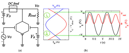
Figure 2.
(a) Schematic of the GFET-based frequency doubler biased by the top gate (vG = Vdirac + vin), drain (VD), and back-gate (VB) voltage sources. The drain bias is provided through a DC feed (to decouple RF and DC components). (b) Operational principle of the GFET frequency doubler: the drain current (ID) and the drain voltage exhibit a quadratic dependency on the gate bias voltage. The output signal at the drain terminal (vd), completes one full oscillation cycle during half a period T of the input signal (vg).
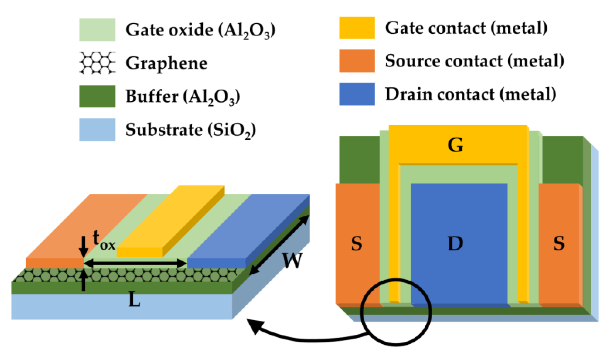
3. The Simulated GFET Device
The circuit simulation of the GFET-based frequency doubler was performed by using the RF design commercial software suite Advanced Design System−ADS® (Keysight Technologies, Inc., Santa Rosa, CA, USA) and a GFET compact model [25]. The adopted model was presented in [26] and validated in [27]. The model reproduced successfully the nonlinear behaviour of GFET-based ambipolar components for RF applications [28,29,30], proving to be a valuable tool for the purpose of predicting the GFET frequency doubler’s performance. The device model considered in our simulations is the top-gated graphene FET described in [19]. Employing an Al2O3 substrate (relative dielectric permittivity εox = 7.5), with higher optical phonon energy compared to traditional SiO2 substrates, the device exhibited enhanced high-frequency performance. This improvement was achieved thanks to the reduced impact on charge carrier saturation velocity of impurities injected into the graphene channel from the substrate. The geometrical parameters and the graphene electronic properties of the simulated top-gate GFET device were taken from [19], which reports mobility up to μ = 2000 cm2 V−1 s−1 and saturation velocity up to vsat = 2 × 107 cm s−1 for a transistor with channel length L = 0.5 μm and width W = 2 × 15 μm. The gate voltage offset VG0 was determined from VG0 = Vdirac − (VD + VS)/2 with Vdirac, VD, VS taken from the drain resistance curve shown in [19]. The surface potential inhomogeneity Δ was fixed considering a fluctuation of ±50 mV [31], corresponding to an energy variation of 0.1 eV. A sketch of the considered device is shown in Figure 3. The complete set of the model input parameters used in the simulations and their description are reported in Table 1.
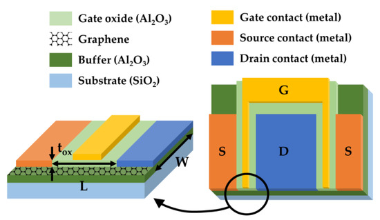
Figure 3.
Sketch of the simulated GFET device described in [19]. On the left, an expanded view of the GFET gate region, corresponding to the circled area on the schematic view of the entire device, shown on the right.

Table 1.
GFET model input parameters.
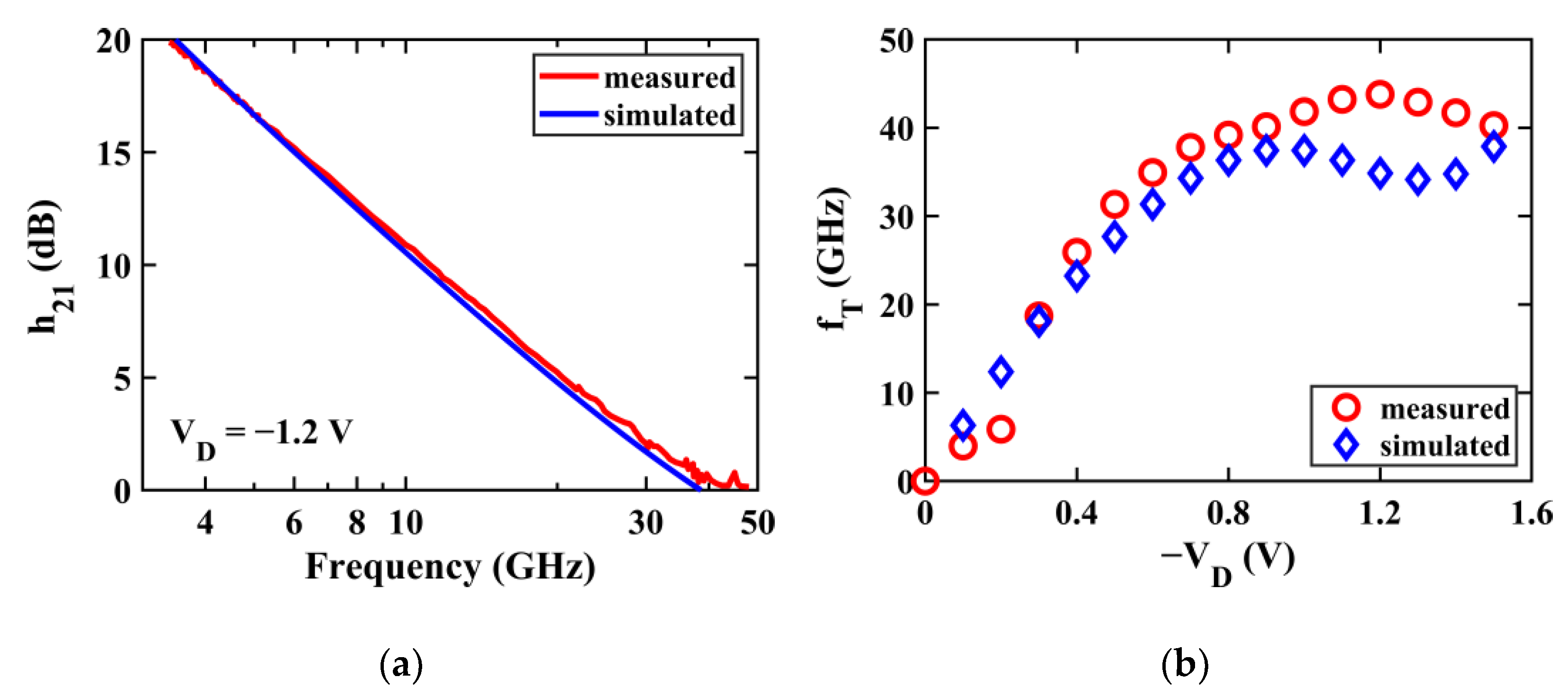
Due to the lack of experimental data concerning the use of the considered GFET in frequency doubling operation, the model performance was compared to the available data reported in [19]. The comparison between the simulated and measured short-circuit current gain, h21, and its transition frequency, fT, computed for increasing values of the drain bias, VD, is shown in Figure 4a and Figure 4b, respectively. The simulations match the experiments quite well, however the model fails to catch the high-frequency behaviour in high-field condition, as can be noticed by the deviation of fT from the measured values when VD > 1 V. This issue is related to the emergence of phenomena linked to the high-field condition which is not accounted for by the GFET compact model. For instance, the effects related to carrier saturation velocity necessitate a more refined model. Moreover, a high drain field induces a non-negligible temperature increase, intensifying the scattering of charge carriers due to their increased interactions with lattice vibrations, impurities, and defects. Additionally, the increase in power consumption amplifies the self-heating of the device, further enhancing the temperature rise and its related effects. These circumstances ultimately lead to a significant impairment of channel mobility, with a consequent impact on the output current. The multifaceted nature of high field condition, therefore, demands more complex models to achieve accurate experimental fitting. To avoid this issue, the following simulations are performed at VD < 0.5 V, in low-field condition.
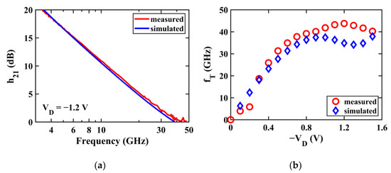
Figure 4.
Simulation-experiment comparison of the short-circuit current gain h21 (a) and its cut-off frequency fT (b) of the considered GFET. Measured data extracted from [19].
It is worth noting that, since the considered device was never characterized as frequency multiplier, the proposed work relies on the consistency of the simulation framework. However, because the adopted model underwent validation for the specific device under consideration (see Figure 4), and for the frequency doubling operation in the time domain [26], we infer that the model can be assumed to describe accurately the combination of this device in frequency doubling operation.
Moreover, the input and output impedance matching networks are intentionally excluded in the performed analysis. By investigating the intrinsic GFET behaviour in frequency doubling operation, the conditions where the device performs more effectively without any other external component are identified. In this way, by exploiting the device functionality at its best, the complexity of matching networks that must be later designed can be reduced, and the design constraints relaxed. This approach allows preserving the simplicity of the circuit, aiming at minimizing the number of components to safeguard footprint, weight, energy consumption, and cost. Furthermore, optimizing the operating conditions to enhance performance of the intrinsic device mitigates the impact of unavoidable parasitic elements (e.g., pad capacitance, contact resistance, interconnect parasitics), which typically impair overall circuit efficiency.
4. Performance of the GFET Frequency Doubler
4.1. Time-Domain Performance Analysis
The circuit shown in Figure 2a was implemented in ADS® and used to analyze the GFET-based frequency doubler performance in the time domain by simulating the schematic shown in Figure 5. The device was biased by setting VG = 2 V, VD = 0.1 V, and grounding the back gate (VB = 0 V). In this way, the GFET was biased at the Dirac point (see Table 1) and in low-field condition. A sinusoidal voltage vin = Vin sin(2πfint) with Vin = 0.3 V and fin = 0.2 MHz, 2 MHz, 20 MHz was provided to the gate terminal, and the output signal was taken across the load resistor RL.
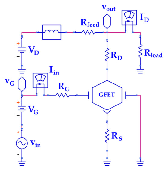
Figure 5.
Schematic of the frequency doubler circuit based on a GFET in common-source configuration. The extrinsic resistances RG, RD, RS are included to represent the contact resistance between graphene and metal, and set according to [19].
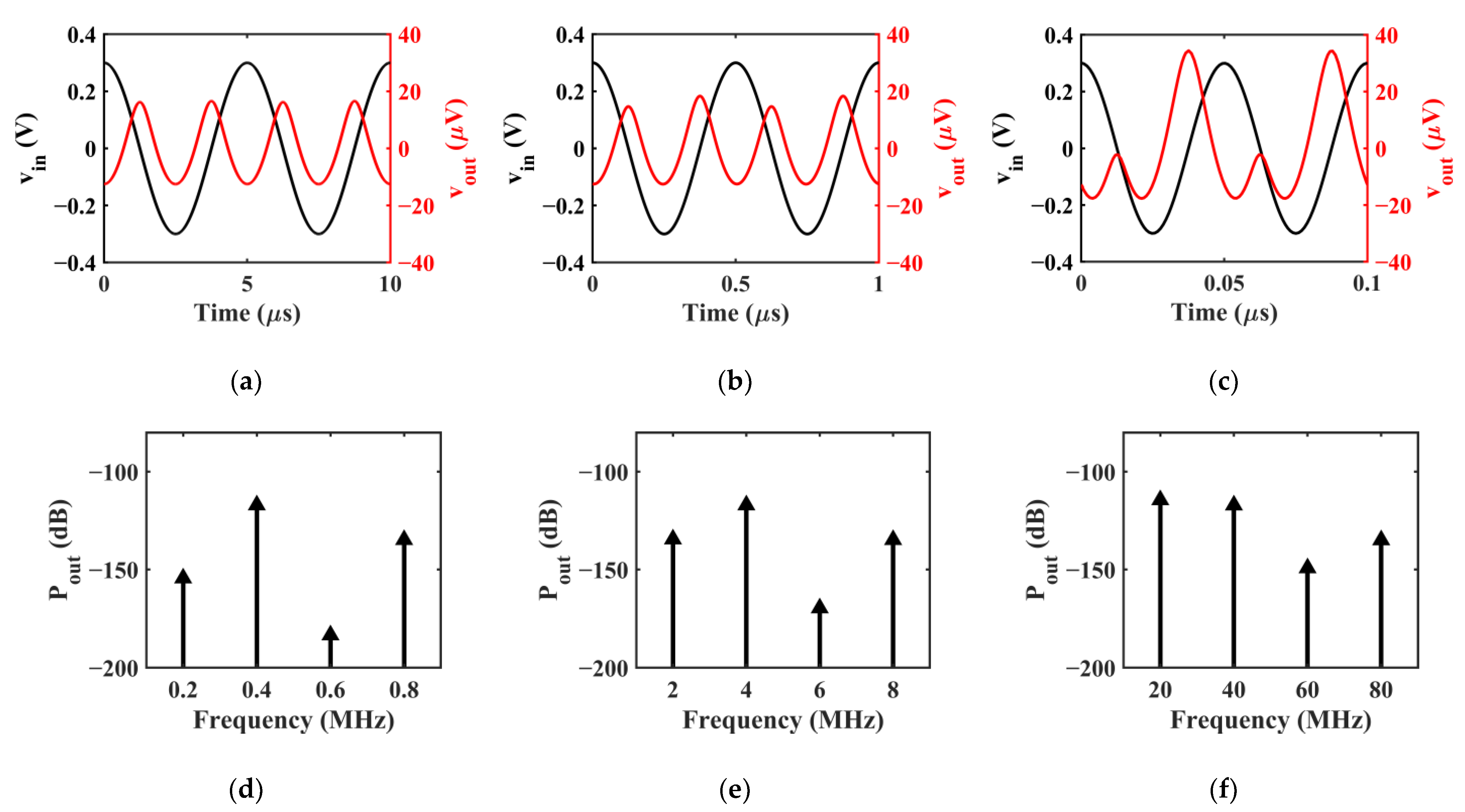
Figure 6 (left side) shows the ac component of the output waveform, vout(t), computed by increasing the fin over three decades. The double-frequency component is clearly dominant in the case of fin = 0.2 MHz, though the voltage gain is very weak due to the low transconductance of the device at the chosen bias point and to the absence of an impedance matching network. In Figure 6 (right side) is shown that, by raising the input signal frequency fin, the power delivered at the double frequency, Pout(2fin), remains approximately unchanged. On the other side, the output power at the fundamental frequency, Pout(fin), changes significantly. This is evident also in the time-domain curves (Figure 6a–c), where the fundamental frequency component becomes increasingly visible on the drain voltage, degrading the purity of the output waveform. At fin = 20 MHz, the fundamental tone amplitude prevails on the second harmonic amplitude, suggesting that the intrinsic device is scarcely efficient for the application to frequency doubling at that frequency.
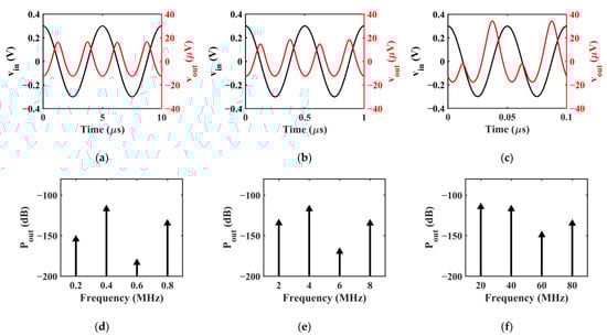
Figure 6.
(a–c) GFET frequency doubler input and output voltage, vin(t) and vout(t), and (d–f) output power, Pout, computed at (a,d) fin = 0.2 MHz, (b,e) fin = 2 MHz, (c,f) fin = 20 MHz.
During normal operation, the fundamental frequency component of the frequency doubler’s output signal is rejected by a high-pass filter, and input and output matching networks enable maximum power transfer to the component, by matching the input impedance, and to the harmonic of interest, by ensuring that the load impedance causes short-circuiting the other harmonics. However, in order to improve the efficiency of the circuit and allow relaxing the complexity of matching networks and filters, it is important to set the operating point where the RF power delivered at the frequency of interest is greater than the power diverted towards other harmonics for the intrinsic device. For this purpose, the power conversion gain CG, defined as the ratio between the output power at twice the input frequency and the input power, according to
and the output power ratio P21, defined as the ratio between the output power delivered at 2fin and the one at fin, as in
can be computed as figures of merit of the frequency doubler performance. The values of CG and P21 corresponding to the data shown in Figure 4, obtained by providing vin = Vin sin(2πfint) with Vin = 0.3 V, are listed in Table 2.
CG = Pout(2fin)/Pin(fin)
P21 = Pout(2fin)/Pout(fin)
Table 2.
CG and P21 at different fin.
4.2. Frequency-Domain Performance Analysis
Since the power ratio P21 is assumed as a figure of merit for the frequency doubler efficiency, its frequency-dependent behaviour is further investigated by performing a harmonic balance (HB) analysis. The HB analysis allows simulating the behaviour of nonlinear circuits excited by large-signal inputs in the frequency domain with good accuracy and low computational effort, because the nonlinear model remains formulated in the time domain but the solution is computed for a specified number of harmonics of the fundamental tone, under the hypothesis of steady-state operation and thus disregarding time transients.
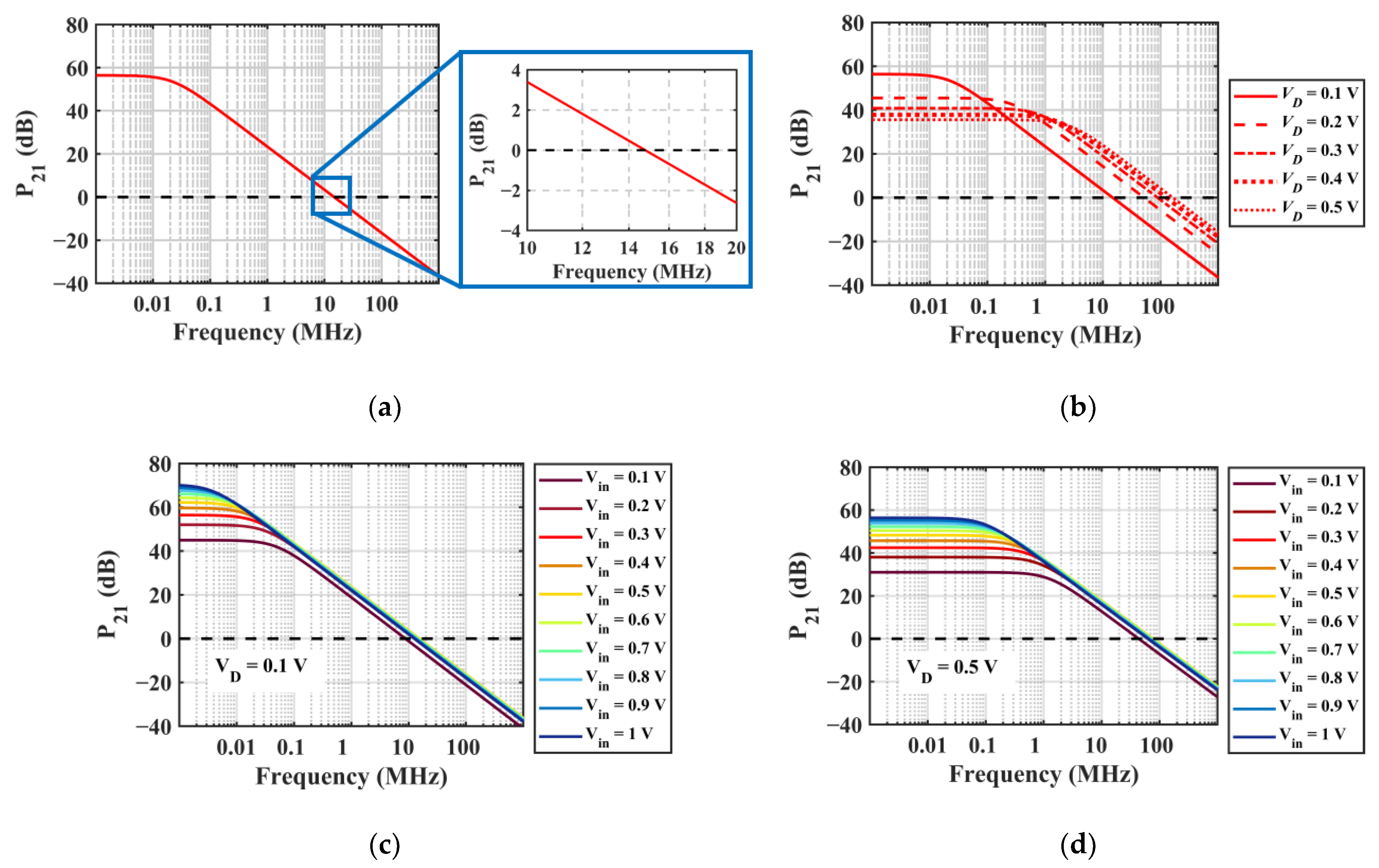
Figure 7a shows the P21 computed when the input signal is a sinusoidal voltage with amplitude Vin = 0.3 V and the frequency sweeps from fin = 1 kHz to fin = 1 GHz. In this way, it is possible to identify the frequency at which the harmonic component at double frequency drops below the fundamental tone, fC. The values of P21 computed by the transient analysis and reported in Table 2 match the results of the HB analysis. The P21 crosses the 0-dB line (i.e., the output power at doubled frequency falls below the output power at the fundamental tone) at the crossing frequency fC ≈ 15 MHz. Considering the current gain of the simulated device (see Figure 4), it is clear that fC is well below the transit frequency in the same static bias condition, fT = 6.3 GHz. Interestingly, these two frequencies are not directly correlated. On one hand, fT represents the maximum frequency at which the GFET can amplify the input current, inversely proportional to the input capacitance and directly proportional to the transconductance, a function of the bias point. On the other hand, the crossing frequency fC represents the highest frequency at which the GFET amplifies the input current while generating higher power at the first harmonic compared to the fundamental tone. The distribution of the output power across the fundamental tone, first-order, and higher-order harmonics depends on the transconductance at the minimum conduction point and at the specific frequency of each harmonic component. Additionally, it also depends on the amplitude of the nonlinear terms in the relationship between IDS and the gate voltage other than the assumed squared dependence. The complex nature of the output power is the reason why it is better computed numerically.
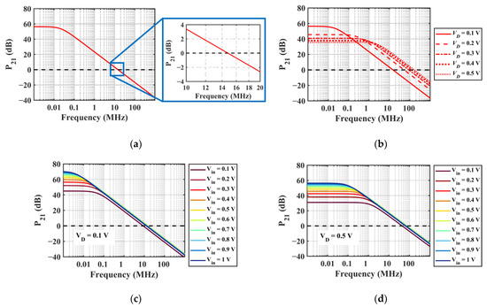
Figure 7.
Frequency dependence of P21 (a) at VD = 0.1 V, and (b) by increasing the drain bias. P21 computed by varying the input signal amplitude in the case of (c) VD = 0.1 V and (d) VD = 0.5 V.
As already assessed for fT and fMAX [18], the value of fC is also strictly related to the operating point, due to the influence of the bias condition on the transconductance and on the input power. It can be noticed, by observing Figure 7b, that the crossing frequency of P21 increases by increasing the drain bias voltage, VD. Thus, the frequency performance of the intrinsic GFET in frequency doubling operation depends on the amplification capabilities of the device, as determined by the fixed bias point. This explains that the small value of VD used in the simulations (VD = 0.1 V) is the reason for the low cut-off frequency fC observed. In addition to the dependence on the bias point, P21 also depends on the input signal amplitude, Vin. Figure 7c,d explore the dependence of P21 on Vin in two different drain bias conditions: VD = 0.1, in Figure 5c; VD = 0.5 V, in Figure 7d (greater values of VD were not considered due to the reduced model accuracy in high-field conditions). It can be seen that the crossing frequency fC is not very much affected by the variation of Vin, whereas the low-frequency value and the bandwidth of P21 change significantly. The P21 dependence on Vin is attributed to the impact of Vin on the input power, Pin, a factor that subsequently affects the output power at both fin and 2fin, and therefore their ratio P21. Moreover, because the frequency multiplication is based on the nonlinear dependence of operation of the drain voltage on the gate voltage (see Figure 2b), increasing Vin triggers nonlinear amplification of the output current and consequently affects the harmonic components of the output power. This altered distribution of energy across higher-order harmonic components reflects in changes of the ratio between Pout(2fin) and Pout(fin), leading to the P21 shown in Figure 7. Finally, harmonic distortion in large-signal operation also leads to conversion gain saturation, further affecting P21.
4.3. Power Conversion Performance Analysis
The efficiency of the GFET frequency doubler can be measured by observing its power conversion gain CG. For the intrinsic device, CG is strongly limited by the GFET input impedance mismatch with both source and load impedance, and can only be improved with tailored matching networks.
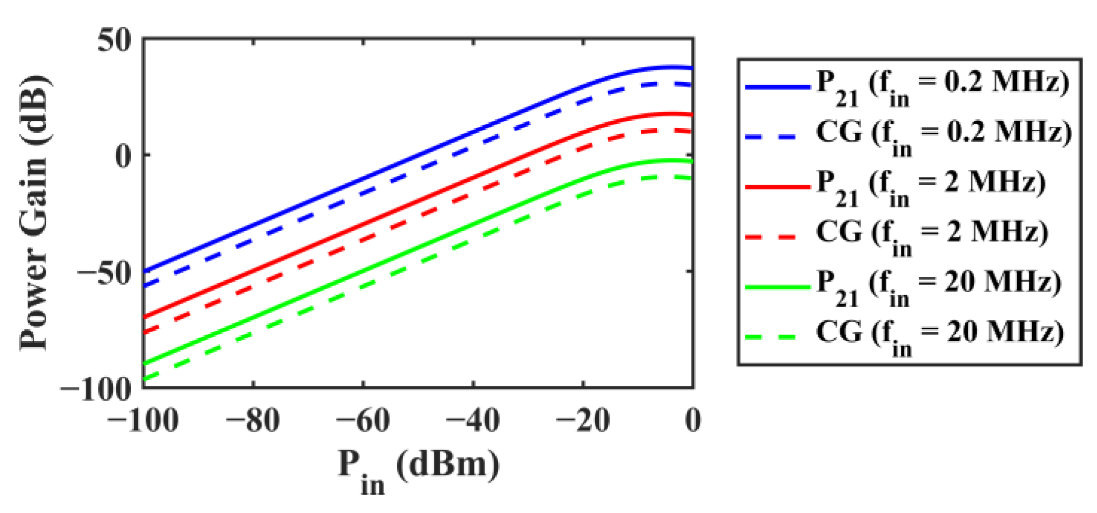
Due to the harmonic distortion introduced by the nonlinear behaviour of transistors in large-signal conditions, increasing the input power above a given threshold leads to saturation of the power conversion gain. It is therefore relevant to consider also the conversion gain saturation when designing the operating conditions of the frequency doubler. Figure 8 reports the simulated P21 and CG computed by harmonic balance analysis while varying the input power, Pin. The simulations were performed using VD = 0.1 V, VG = 2 V, and considering the input signal frequencies fin = 0.2 MHz, 2 MHz, 20 MHz. In accordance with the expectation, both P21 and CG increase with a +10 dB/dec slope. For the considered device, the saturation of the output power starts around Pin ~ −10 dBm (100 μW), and the curves reach the maximum value at Pin,sat. This value is reportedly affected also by the device contact resistance [7].
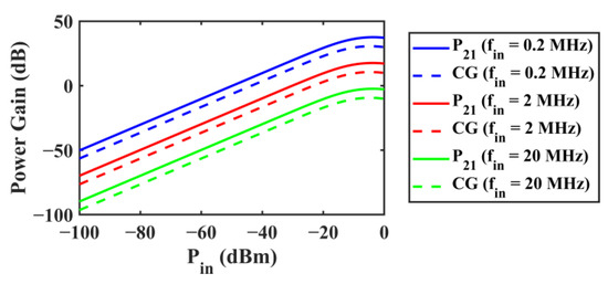
Figure 8.
Simulated power gain P21 and CG plotted against Pin for fin = 0.2 MHz, 2 MHz, 20 MHz. Saturation appears above Pin ~ −10 dBm.
5. Discussion
The proposed work supports the design of GFET-based frequency doublers for application to signal modulation systems in the MHz-range, such as harmonic transponders and integrated sensing and modulation systems. Based on the findings presented in Section 4, concerning the performance of a recent GFET device in frequency doubling operation, informed criteria for the selection of the optimal operating conditions can be obtained. In particular, the results of this study restrict the range of frequencies for selecting the operating frequency of the system to those in which the device demonstrates higher efficiency, and provides information that can guide the shaping the input signal interrogating the sensor.
Indeed, the design of nonlinear circuits for frequency multiplication starts with the optimization of the bias levels. To operate as frequency multiplier, the GFET must be biased at the Dirac point, posing a first constraint on the gate bias. Following the analysis reported in Figure 7b, it becomes evident that increasing the drain voltage is advantageous when the specific application demands a shift towards higher frequencies. This adjustment allows enhancing the rejection of the fundamental tone by design. Once the static operating condition is fixed, the input signal can be tailored.
Both the amplitude and frequency of the input signal can be set aiming at maximizing the device performance. To improve the power conversion efficiency of the intrinsic device, the most suitable operating frequency can be fixed based on the P21 bandwidth (see Figure 7b). It is important to bear in mind, during this phase, that increasing the frequency unavoidably worsens the power conversion gain, regardless of the input signal power level, as can be seen in Figure 6. After fixing the signal frequency, appropriate measures for output impedance matching can be implemented, so that undesired harmonic components can be effectively driven through low-impedance paths (ideally, short-circuited) and the power transfer from the input to the double-frequency harmonic component can be enhanced. Concerning the input signal level, Figure 7c,d show that higher amplitude of the input signal supports higher rejection of the fundamental tone, and improves the conversion gain through the greater input power, as proven by Figure 8. However, it is worth noting that high amplitude of the input signal may lead to greater harmonic distortion due to the nonlinear behaviour in large-signal operation of the GFET. Figure 8 shows that this may lead to saturation of the conversion gain. Therefore, the input signal amplitude should be set to achieve an input power level, based on the chosen operating frequency, that prevents saturation of the conversion gain.
Finally, the doubler should be cascaded with high-pass filters to remove the DC offset and enhance the rejection of the fundamental tone, and eventually with selective filters to relax the requirements on the impedance matching networks.
Although the operating conditions can be designed to maximize the efficiency of the GFET for its specific use as frequency doubler, it is worth discussing also the open issues related to the use of GFETs, and more broadly of graphene components, for the proposed application. Currently, the performance of GFETs in terms of amplification properties and maximum operating frequency still lags behind state-of-the-art components, mainly due to the poor conversion gain and impurity-related impairments. Moreover, shifting from traditional electronics to all-graphene electronics will require technological improvements in the manufacturing and transfer of graphene, to enhance the reliability and repeatability of graphene components. Nevertheless, simulation works suggest new possibilities and applications not affordable by traditional technology, inspiring the exploration of innovative solutions to overcome current technological limitations and drive graphene electronics towards its full potential.
6. Conclusions
This work investigated the performance of a single-device GFET-based frequency doubler by means of circuit simulations. The observed performance indicators include the ratio between the output power at double-frequency and that at fundamental frequency, and the power conversion gain at double frequency. The performed analysis offers guidelines for the design of operating conditions that maximize the device efficiency, thereby relaxing constraints on signal conditioning circuits and impedance matching networks. By providing the knowledge required to perform the tuning of the GFET frequency doubler design, the findings of this study can support the development of all-graphene sensing, modulation, and transmission systems. This study, combined with the envisioned future research directions, aims to contribute to the ongoing technological transition towards lightweight, small, thermally-efficient, power-saving carbon-based components for the pervasive Internet-of-Everything scenario. Future research will focus on the analysis of the frequency doubler’s robustness against fabrication-related uncertainties, addressing the concern about the process-induced non-uniformity of the device performance. Further, the development of criteria for designing input and output impedance matching network will be investigated, based on the latest advancements in graphene passive components. Finally, the GFET frequency doubler’s integration into highly-efficient and compact all-graphene systems will be explored.
Author Contributions
Conceptualization, M.L.M., P.L. and V.T.; methodology, M.L.M.; software, M.L.M.; validation, M.L.M., P.L. and V.T.; investigation, M.L.M.; resources, P.L.; data curation, M.L.M.; writing—original draft, M.L.M.; writing—review and editing, M.L.M. and V.T.; visualization, M.L.M.; supervision, P.L. and V.T.; project administration, P.L.; funding acquisition, P.L. All authors have read and agreed to the published version of the manuscript.
Funding
This work has received funding from the European Union’s Horizon 2020 research and innovation programme under Graphene Flagship grant agreement No 881603, and from the European Union’s NextGenerationEU programme through the Italian National Recovery and Resilience Plan (NRRP) programme under PRIN-PNRR-2022 UPWARDS CUP E53D23014490001.
Data Availability Statement
The original contributions presented in the study are included in the article, further inquiries can be directed to the corresponding author.
Acknowledgments
The authors acknowledge Francisco Pasadas Cantos for providing the Verilog-A compact model for the circuital analysis of the GFET.
Conflicts of Interest
The authors declare no conflicts of interest. The funders had no role in the design of the study; in the collection, analyses, or interpretation of data; in the writing of the manuscript; or in the decision to publish the results.
References
- La Mura, M.; Cassioli, D.; Shundalau, M.; Cianca, E.; Lamberti, P. Graphene Devices for Aerial Wireless Communications at THz. IOP Conf. Ser. Mater. Sci. Eng. 2024, in press.
- Wang, H.; Hsu, A.L.; Palacios, T. Graphene electronics for RF applications. IEEE Microw. Mag. 2012, 13, 114–125. [Google Scholar] [CrossRef]
- Lamberti, P.; la Mura, M.; Pasadas, F.; Jiménez, D.; Tucci, V. Tolerance analysis of a GFET transistor for aerospace and aeronautical application. IOP Conf. Ser. Mater. Sci. Eng. 2021, 1024, 012005. [Google Scholar] [CrossRef]
- Wang, H.; Nezich, D.; Kong, J.; Palacios, T. Graphene Frequency Multipliers. IEEE Electron Device Lett. 2009, 30, 547–549. [Google Scholar] [CrossRef]
- Wang, Z.; Zhang, Z.; Xu, H.; Ding, L.; Wang, S.; Peng, L.M. A high-performance top-gate graphene field-effect transistor based frequency doubler. Appl. Phys. Lett. 2010, 96, 173104. [Google Scholar] [CrossRef]
- Wang, H.; Hsu, A.; Kim, K.K.; Kong, J.; Palacios, T. Gigahertz ambipolar frequency multiplier based on CVD graphene. In Proceedings of the 2010 International Electron Devices Meeting, San Francisco, CA, USA, 6–8 December 2010; pp. 23.6.1–23.6.4. [Google Scholar]
- Ramón, M.E.; Parrish, K.N.; Chowdhury, S.F.; Magnuson, C.W.; Movva, H.C.P.; Ruoff, R.S.; Banerjee, S.K.; Akinwande, D. Three-Gigahertz Graphene Frequency Doubler on Quartz Operating Beyond the Transit Frequency. IEEE Trans. Nanotechnol. 2012, 11, 877–883. [Google Scholar] [CrossRef]
- Wang, H.; Hsu, A.; Mailly, B.; Kim, K.K.; Kong, J.; Palacios, T. Towards ubiquitous RF electronics based on graphene. In Proceedings of the IEEE MTT-S International Microwave Symposium Digest, Montreal, QC, Canada, 17–22 June 2012. [Google Scholar] [CrossRef]
- Chen, H.Y.; Appenzeller, J. Graphene-based frequency tripler. Nano Lett. 2012, 12, 2067–2070. [Google Scholar] [CrossRef]
- Cheng, C.; Huang, B.; Mao, X.; Zhang, Z.; Zhang, Z.; Geng, Z.; Xue, P.; Chen, H. A graphene based frequency quadrupler. Sci. Rep. 2017, 7, 46605. [Google Scholar] [CrossRef]
- Norhakim, N.; Hawari, H.F.; Burhanudin, Z.A. Assessing the Figures of Merit of Graphene-Based Radio Frequency Electronics: A Review of GFET in RF Technology. IEEE Access 2022, 10, 17030–17042. [Google Scholar] [CrossRef]
- La Mura, M.; Lamberti, P.; Tucci, V. Numerical Evaluation of the Effect of Geometric Tolerances on the High-Frequency Performance of Graphene Field-Effect Transistors. Nanomaterials 2021, 11, 3121. [Google Scholar] [CrossRef] [PubMed]
- Zhan, B.; Li, C.; Yang, J.; Jenkins, G.; Huang, W.; Dong, X. Graphene field-effect transistor and its application for electronic sensing. Small 2014, 10, 4042–4065. [Google Scholar] [CrossRef]
- Sreejith, S.; Ajayan, J.; Radhika, J.M.; Sivasankari, B.; Tayal, S.; Saravanan, M. A comprehensive review on graphene FET bio-sensors and their emerging application in DNA/RNA sensing & rapid Covid-19 detection. Meas. J. Int. Meas. Confed. 2023, 206, 112202. [Google Scholar]
- Krishnan, S.K.; Nataraj, N.; Meyyappan, M.; Pal, U. Graphene-Based Field-Effect Transistors in Biosensing and Neural Interfacing Applications: Recent Advances and Prospects. Anal. Chem. 2023, 95, 2590–2622. [Google Scholar] [CrossRef] [PubMed]
- Huang, H.; Sakhdari, M.; Hajizadegan, M.; Shahini, A.; Akinwande, D.; Chen, P.Y. Toward transparent and self-activated graphene harmonic transponder sensors. Appl. Phys. Lett. 2016, 108, 173503. [Google Scholar] [CrossRef]
- Hajizadegan, M.; Sakhdari, M.; Zhu, L.; Cui, Q.; Huang, H.; Cheng, M.M.C.; Hung, J.C.H.; Chen, P.Y. Graphene Sensing Modulator: Toward Low-Noise, Self-Powered Wireless Microsensors. IEEE Sens. J. 2017, 17, 7239–7247. [Google Scholar] [CrossRef]
- La Mura, M.; Lamberti, P.; Tucci, V. Simulation of Graphene-based Materials and Devices for Sub-Terahertz Applications. In Proceedings of the 2023 IEEE Nanotechnology Materials and Devices Conference, Paestum, Italy, 22–25 October 2023; pp. 901–905. [Google Scholar] [CrossRef]
- Asad, M.; Jeppson, K.O.; Vorobiev, A.; Bonmann, M.; Stake, J. Enhanced High-Frequency Performance of Top-Gated Graphene FETs Due to Substrate- Induced Improvements in Charge Carrier Saturation Velocity. IEEE Trans. Electron Devices 2021, 68, 899–902. [Google Scholar] [CrossRef]
- Han, S.J.; Reddy, D.; Carpenter, G.D.; Franklin, A.D.; Jenkins, K.A. Current saturation in submicrometer graphene transistors with thin gate dielectric: Experiment, simulation, and theory. ACS Nano 2012, 6, 5220–5226. [Google Scholar] [CrossRef]
- Pasadas, F.; Medina-Rull, A.; Feijoo, P.C.; Pacheco-Sanchez, A.; Marin, E.G.; Ruiz, F.G.; Rodriguez, N.; Godoy, A.; Jiménez, D. Unveiling the impact of the bias-dependent charge neutrality point on graphene based multi-transistor applications. Nano Express 2021, 2, 036001. [Google Scholar] [CrossRef]
- Parrish, K.N.; Akinwande, D. Even-odd symmetry and the conversion efficiency of ideal and practical graphene transistor frequency multipliers. Appl. Phys. Lett. 2011, 99, 223512. [Google Scholar] [CrossRef]
- Meric, I.; Han, M.Y.; Young, A.F.; Ozyilmaz, B.; Kim, P.; Shepard, K.L. Current saturation in zero-bandgap, top-gated graphene field-effect transistors. Nat. Nanotechnol. 2008, 3, 654–659. [Google Scholar] [CrossRef]
- Schwierz, F. Graphene transistors. Nat. Nanotechnol. 2010, 5, 487–496. [Google Scholar] [CrossRef]
- Pasadas, F.; Feijoo, P.C.; Mavredakis, N.; Pacheco-Sanchez, A.; Chaves, F.A.; Jiménez, D. Compact Modeling Technology for the Simulation of Integrated Circuits Based on Graphene Field-Effect Transistors. Adv. Mater. 2022, 34, 2201691. [Google Scholar] [CrossRef] [PubMed]
- Pasadas, F.; Jimenez, D. Large-Signal Model of Graphene Field-Effect Transistors—Part I: Compact Modeling of GFET Intrinsic Capacitances. IEEE Trans. Electron Devices 2016, 63, 2936–2941. [Google Scholar] [CrossRef]
- Pasadas, F.; Jiménez, D. Large-Signal Model of Graphene Field- Effect Transistors—Part II: Circuit Performance Benchmarking. IEEE Trans. Electron Devices 2016, 63, 2942–2947. [Google Scholar] [CrossRef]
- Pacheco-Sanchez, A.; Ramos-Silva, J.N.; Mavredakis, N.; Ramirez-Garcia, E.; Jimenez, D. Exploiting the ambipolarity in emerging transistors for high-frequency applications. In Proceedings of the 2022 37th Conference on Design of Circuits and Integrated Circuits, Pamplona, Spain, 16–18 November 2022; pp. 1–6. [Google Scholar] [CrossRef]
- Pasadas, F.; Medina-Rull, A.; Ruiz, F.G.; Ramos-Silva, J.N.; Pacheco-Sanchez, A.; Pardo, M.C.; Toral-Lopez, A.; Godoy, A.; Ramírez-García, E.; Jiménez, D.; et al. Exploiting Ambipolarity in Graphene Field-Effect Transistors for Novel Designs on High-Frequency Analog Electronics. Small 2023, 19, 2303595. [Google Scholar] [CrossRef] [PubMed]
- Toral-Lopez, A.; Marin, E.G.; Pasadas, F.; Ganeriwala, M.D.; Ruiz, F.G.; Jiménez, D.; Godoy, A. Reconfigurable frequency multipliers based on graphene field-effect transistors. Discov. Nano 2023, 18, 123. [Google Scholar] [CrossRef]
- Martin, J.; Akerman, N.; Ulbricht, G.; Lohmann, T.; Smet, J.H.; Von Klitzing, K.; Yacoby, A. Observation of electron–hole puddles in graphene using a scanning single-electron transistor. Nat. Phys. 2007, 4, 144–148. [Google Scholar] [CrossRef]

Disclaimer/Publisher’s Note: The statements, opinions and data contained in all publications are solely those of the individual author(s) and contributor(s) and not of MDPI and/or the editor(s). MDPI and/or the editor(s) disclaim responsibility for any injury to people or property resulting from any ideas, methods, instructions or products referred to in the content. |
© 2024 by the authors. Licensee MDPI, Basel, Switzerland. This article is an open access article distributed under the terms and conditions of the Creative Commons Attribution (CC BY) license (https://creativecommons.org/licenses/by/4.0/).