
Design of Lossless Negative Capacitance Multiplier Employing a Single Active Element


1
Department of Electrical—Electronics Engineering, İstanbul University-Cerrahpaşa, Avcılar, İstanbul 34320, Türkiye
2
Vocational School of Technical Sciences, İstanbul University-Cerrahpaşa, Büyükçekmece, İstanbul 34500, Türkiye
*
Author to whom correspondence should be addressed.
Electronics 2024, 13(6), 1163; https://doi.org/10.3390/electronics13061163
Submission received: 21 February 2024
/
Revised: 14 March 2024
/
Accepted: 15 March 2024
/
Published: 21 March 2024
Abstract
:In this paper, a new negative lossless grounded capacitance multiplier (GCM) circuit based on a Current Feedback Operational Amplifier (CFOA) is presented. The proposed circuit includes a single CFOA, four resistors, and a grounded capacitor. In order to reduce the power consumption, the internal structure of the CFOA is realized with dynamic threshold-voltage MOSFET (DTMOS) transistors. The effects of parasitic components on the operating frequency range of the proposed circuit are investigated. The simulation results were obtained with the SPICE program using 0.13 µm IBM CMOS technology parameters. The total power consumption of the circuit was 1.6 mW. The functionality of the circuit is provided by the capacitance cancellation circuit. PVT (Process, Voltage, Temperature) analyses were performed to verify the robustness of the proposed circuit. An experimental study is provided to verify the operability of the proposed negative lossless GCM using commercially available integrated circuits (ICs).
1. Introduction
High-value capacitors in IC technology require a large silicon area. To address this issue, capacitance multiplier (CM) circuits capable of multiplying capacitance have been proposed to obtain large capacitance from small capacitance values. Therefore, CM circuits play an essential role in obtaining high-value capacitances.
CM circuits can be classified as grounded [1,2,3,4,5,6,7,8] and floating [9,10,11,12,13,14,15,16,17,18] according to the type of the simulated capacitance, and positive [1,2,3,4,5,6,7] and negative [19,20,21,22,23,24,25,26,27,28] according to the value of the simulated capacitance.
A literature survey reveals that there are various CM circuits are reported using numerous versatile active building blocks (ABBs). However, upon careful examination of the circuit configurations published in the literature, they are considered to suffer from some of the limitations given below.
- The circuits implemented with two or more active and passive elements have higher power consumption and a larger area on the chip.
- They are practically not applicable with commercially available ICs.
- The multiplication factor is not electronically adjustable.
Four negative CFOA-based CM circuit topologies have been proposed by Lahiri and Gupta [19]. While the first two proposed circuits contain two CFOAs, the other circuits consist of a single CFOA. All circuits are designed using two resistors and a single capacitor. Additionally, the circuits do not require any critical component matching conditions. All of the circuits in SPICE have been tested using the AD844 macro model. A capacitance cancellation circuit and a quadratic oscillator circuit are given as application examples. The resistance-controlled negative capacitance multiplier circuit presented by Abuelma’atti and Dhar consists of two CFOAs, two floating resistors, and a floating capacitor [20]. The negative CM circuit proposed by Dogan and Yuce includes a single CFOA, three resistors, and a capacitor [21]. The circuit proposed by Al-Absi and Abuelma’atti includes one CFOA and two OTAs. It is configured as an OTA-negative resistor to achieve an adjustable negative impedance multiplier [22]. The resistor-free circuit presented by Stornelli et al. consists of an E-VCII- and a capacitor [23].
Many of the negative CMs available in the literature contain two or more ABBs [19,20,22,24,25,27,28]. There are also circuits that contain only one active device [19,21,23,26,29,30,31]. When designing negative CMs, excessive use of active and passive elements should be avoided as this will increase power consumption. Negative CMs presented by researchers have generally been realized through the use of three or more passive elements [19,20,21,24,25,28,30,31]. Negative CMs containing a single capacitor have also been proposed, but each of these circuits operates with two or more active components [22,27].
The aim of this work was to design a negative lossless GCM circuit using currently commercially available ICs, namely the AD844 [32]. The proposed circuit is designed with a single CFOA, four resistors and a grounded capacitor. The internal structure of the CFOA is built with DTMOS transistors to reduce power consumption. The total power consumption of the circuit is 1.6 mW. The non-ideal analysis for the proposed circuit has been investigated in detail. A capacitance cancellation circuit is presented as an application example. To verify the operability of the proposed circuit, it has been experimentally tested using commercially available ICs, namely AD844s.
2. The Proposed Circuit
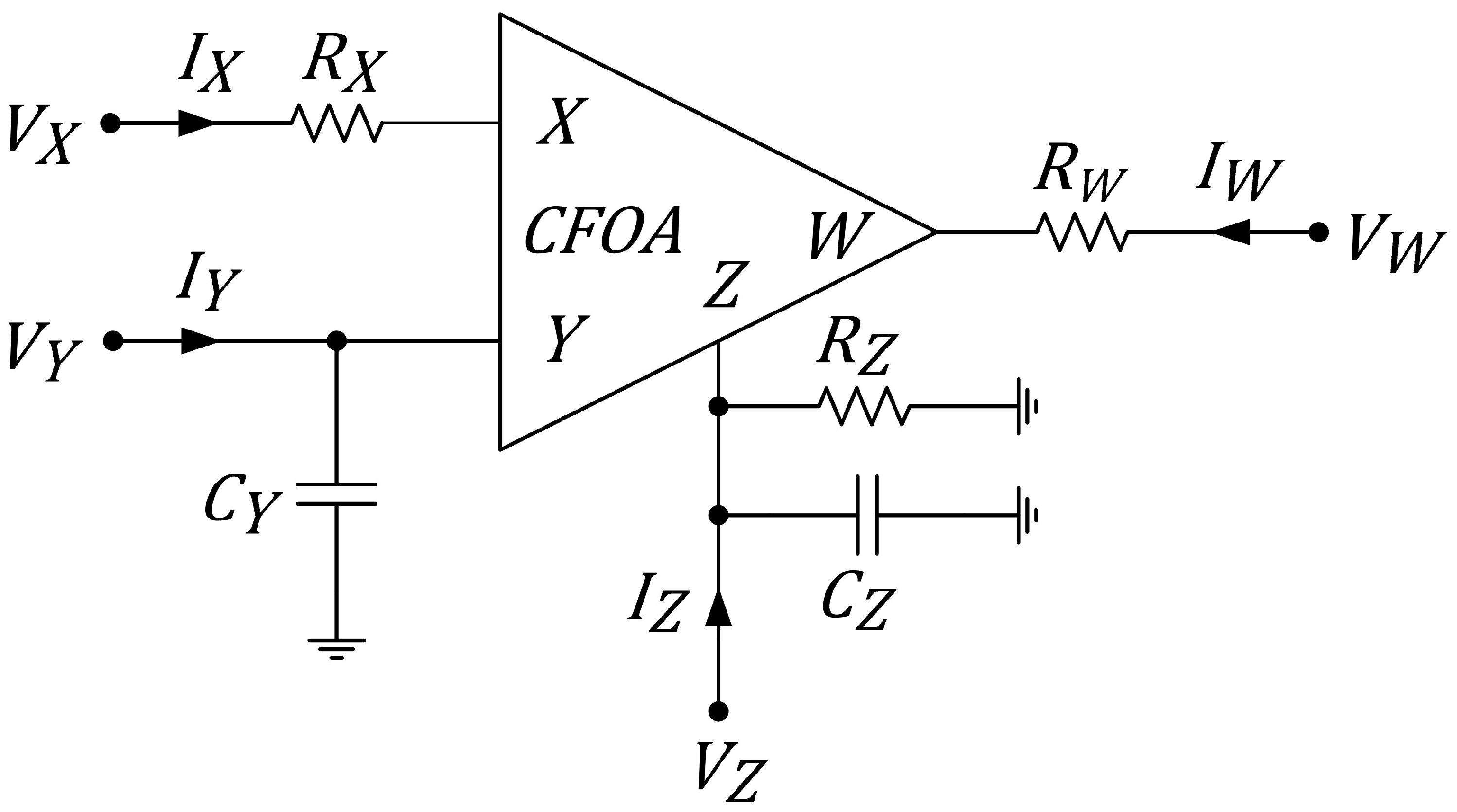
The terminal relations of CFOAs, whose circuit symbol and equivalent circuit are given in Figure 1 and Figure 2, respectively, can be represented in the following matrix equation:
where α(s) represents the current gain which is ideally equal to unity. Also, the β(s) and η(s) correspond to voltage gains and ideally both of them are equal to unity. Furthermore, α(s), β(s), and η(s) can be given by
Herein, represents the current-tracking error, ideally equal to zero, while and denote the voltage tracking errors, also ideally equal to zero. It is assumed that , , and are significantly smaller than one.
In addition, , , and denote corner frequencies of the relevant parameter. Furthermore, in an ideal case, Rin is infinity and the port relationships of the CFOA are expressed by the following equations: VX = VY, IY = 0, IZ = IX, and VW = VZ.
The proposed negative lossless GCM is depicted in Figure 3. Without passive element matching conditions, the input admittance (Yin) of the circuit is obtained as follows:
If R2 = R1 is selected for the circuit in Figure 3, the input admittance is simplified as follows. When this condition is met, the circuit can simulate negative lossless GCM. The equivalent capacitance (Ceq) and the multiplication factor (K) are given by
As can be seen from Equation (8), if one of the resistors R3 or R4 is replaced with an MOS-based voltage-controlled resistor, the multiplication factor becomes electronically controllable.
The sensitivity of the K with respect to the tuning resistors is given below.
3. Non-Ideal Analysis
The non-ideal equivalent circuit of a CFOA is shown in Figure 4. Here, RX, RZ, and RW indicate parasitic resistors. Also, CY and CZ demonstrate the parasitic capacitors. Ideally, these parasitic elements are RX = RW = CZ = CY = 0 and RZ = ꝏ. The terminal relations of the CFOA in non-ideal conditions are given in Equation (12).
Taking into account the effects of the non-ideal gains of the CFOA, the input admittance of the circuit is obtained as follows.
Considering the non-ideal gains of the CFOA, the equivalent circuit of the proposed circuit is given in Figure 5; the values of the equivalent components are given in Equations (14)–(16).
The sensitivity analysis is given below.
Under the specified condition where only the parasitic impedances of the X, Y, Z, and W terminals are considered, the input admittance is derived in the form presented in Equation (22).
In this context, ai and bi represent the real coefficients of the driving point admittance Yin(s).
In the ideal case, the input admittance of the capacitor is of the form Yin(s) = a1s/b0. To obtain a lossless capacitor, the terms other than a1s and b0 need to be small enough. In other terms, when s is substituted with jω, the following inequalities must be concurrently fulfilled to approximate the ideal capacitor admittance:
According to the inequalities given above, the operating frequency range of the proposed circuit is calculated approximately as follows.
4. Simulation Results
In order to reduce the power consumption of analog integrated circuits, operations with lower supply voltages can be provided by DTMOS technology [33,34,35,36,37]. To obtain a DTMOS transistor, the body and gate terminals of the MOSFET are short-circuited as shown in Figure 6. The DTMOS-based implementation of the CFOA, derived from the CCII+ presented in reference [38], is depicted in Figure 7.
The simulation results have been obtained utilizing the SPICE program, employing 0.13 µm IBM CMOS technology parameters. The power supply and bias voltage were chosen as VDD = −VSS = 0.6 V and VB = −0.2 V, respectively. The transistor dimensions are detailed in Table 1. The parasitic impedances and non-ideal gains of the CFOA are delineated in Table 2.
The functionality of the proposed negative GCM was examined under the following simulation conditions. Detailed simulation settings are included in Table 3.
- (i)
- Multiplication factor (K) is constant while C is variable;
- (ii)
- C is constant while K is variable.

Table 3.
Detailed simulation results and passive component settings.
| Case | Passive Components | K | Ceq (nF) | Frequency Response | |||||
|---|---|---|---|---|---|---|---|---|---|
| C (nF) | R1 (kΩ) | R2 (kΩ) | R3 (Ω) | R4 (kΩ) | Magnitude within 10% Error | Phase within 10° Error | |||
| 1 | 0.1 | 10 | 10 | 100 | 1 | −10 | −1 | 4 Hz to 80 MHz | 14 Hz to 53 MHz |
| 10 | 10 | 100 | 10 | −50.5 | −5.05 | 9 Hz to 35 MHz | 52 Hz to 47 MHz | ||
| 10 | 10 | 10 | 10 | −500.5 | 50.05 | 9 Hz to 32 MHz | 53 Hz to 11 MHz | ||
| 2 | 0.5 | 10 | 10 | 100 | 1 | −10 | −5 | 1 Hz to 52 MHz | 3 Hz to 30 MHz |
| 5 | −50 | 1 Hz to 20 MHz | 1 Hz to 15 MHz | ||||||
| 50 | −500 | 1 Hz to 4.5 MHz | 1 Hz to 4.5 MHz | ||||||
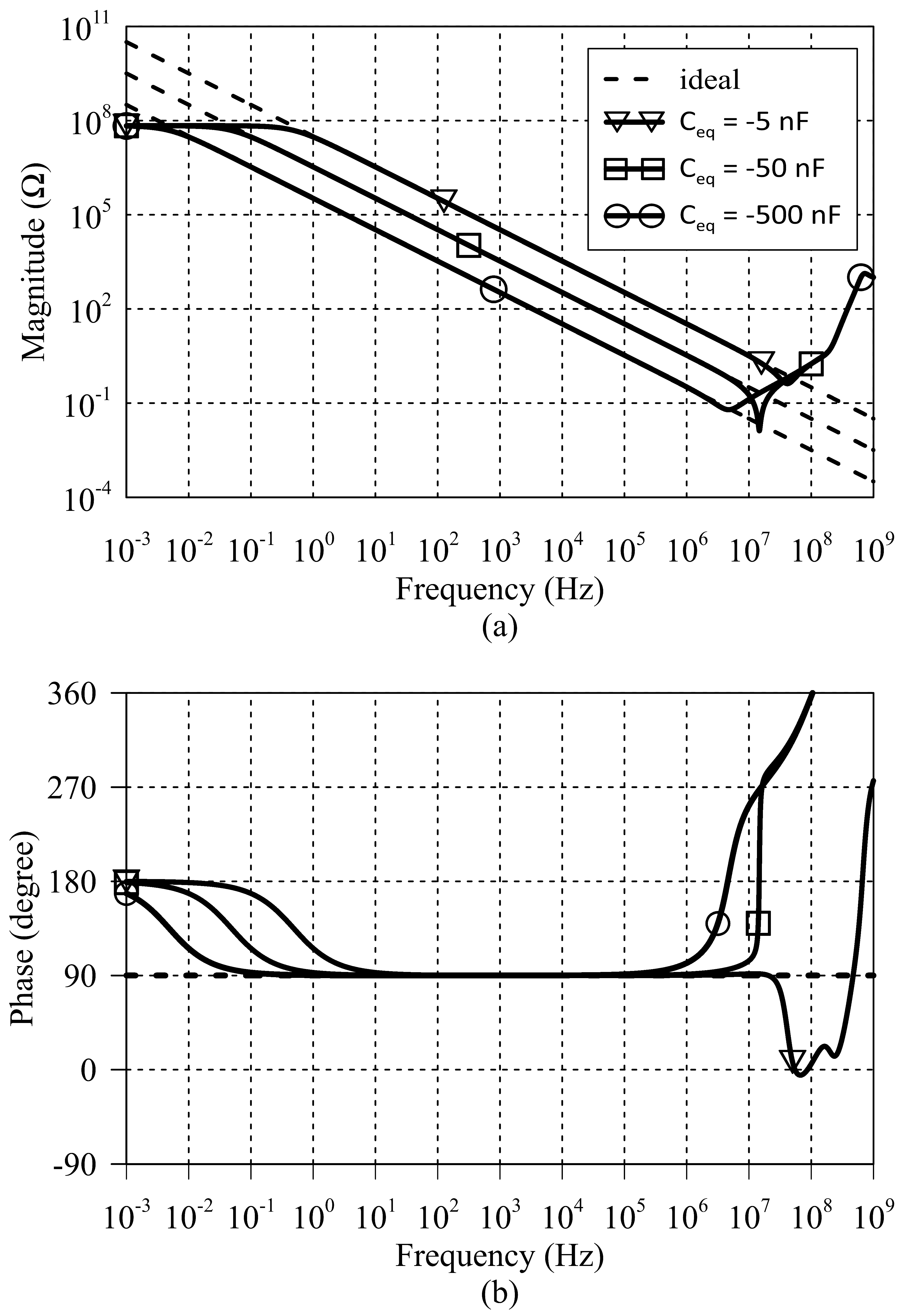
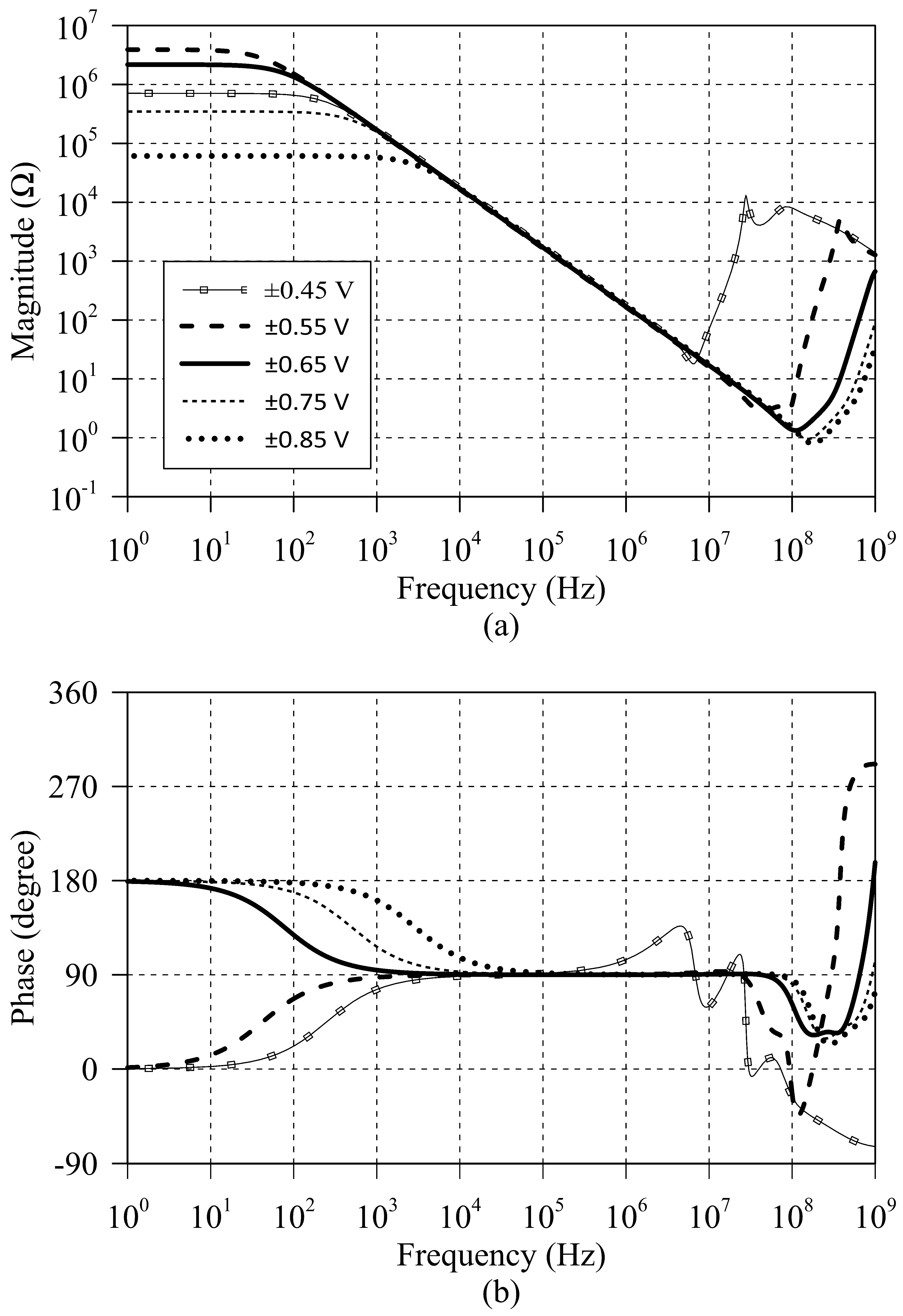
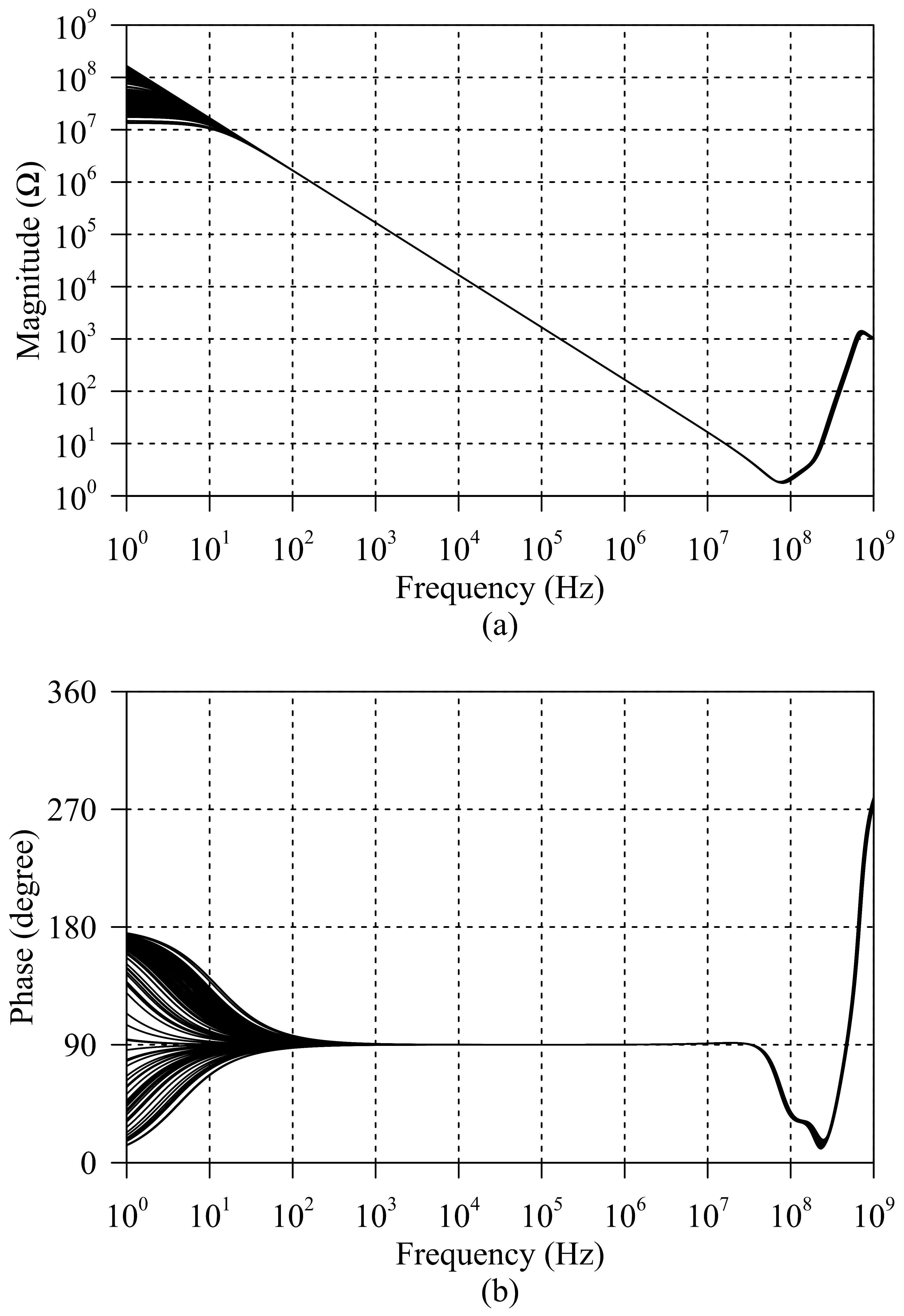
The frequency response of the input impedance of the proposed negative lossless GCM is given in Figure 8 for various multiplication factors (K). By selecting the passive elements as , , , , , and , the multiplication factors are set to , , and , resulting in Ceq = −1 nF, −5.05 nF, and −50.05 nF, respectively. In Figure 9, a comparison of the proposed negative GCM with the ideal capacitor for Ceq = 5, 50, and 500 nF is given by selecting K = 10, C = 0.5, 5, and 50 nF, respectively. The frequency responses of the proposed circuit to various supply voltages are shown in Figure 10. Monte Carlo (MC) simulations were conducted for 100 runs. The simulation results for a 10% change in the threshold voltages and gate oxide thicknesses of all MOS transistors and a 5% change in the width of all MOS transistors are shown in Figure 11 and Figure 12, respectively. A temperature analysis of the circuit is also depicted in Figure 13.
A table of comparisons of previously reported negative CM circuits using various ABBs can be seen in Table 4. The proposed circuit contains a single CFOA. Compared to other circuits implemented with a single active component, the number of passive elements is relatively high. However, to reduce power consumption, the internal structure of the CFOA is designed using the DTMOS technique. Power consumption can be reduced by using MOS-based resistors. The multiplication factor of the circuit can be adjusted up to 500. In addition, according to Figure 8, the operating frequency reaches 80 MHz. Considering its simplicity, operating frequency, and multiplication factor, it is clear that the proposed circuit is superior to the circuits in the literature.
5. Application Example
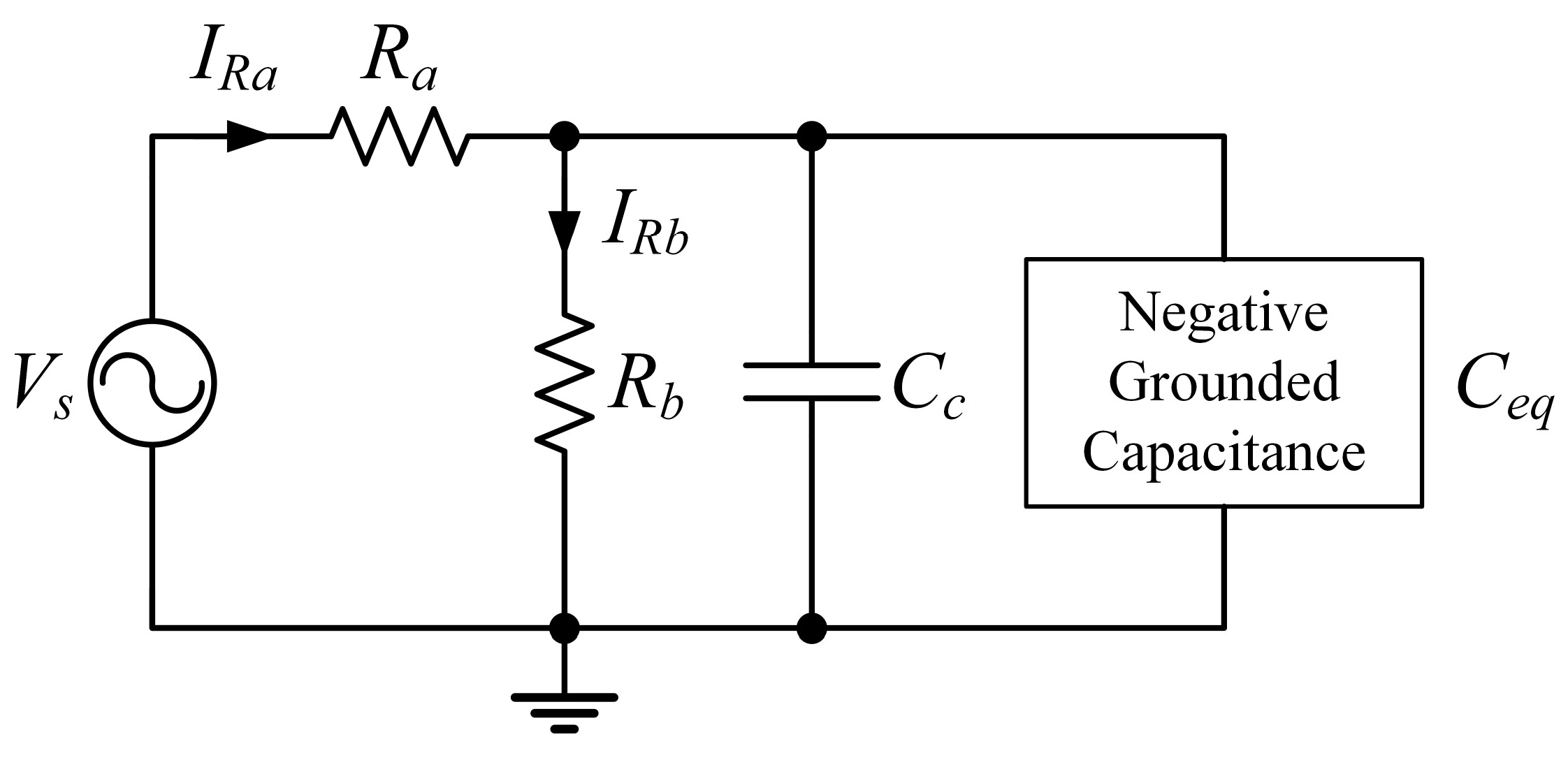
This section presents an application example to demonstrate the robustness and workability of the proposed GCM. The application example shown in Figure 14 is the capacitive cancellation circuit in which the parasitic capacitors in the output circuits are eliminated. Here, the negative capacitor (Ceq) is obtained with the proposed negative lossless GCM. The resistance currents and in the circuit are given below. If the condition is satisfied, and will be equal.
The simulation result was obtained by choosing and . The proposed negative GCM is designed to have in the circuit by choosing and . The frequency performance of the capacitance cancellation circuit, for the output current , is given in Figure 15. According to the results, the circuit is compatible with ideal results up to 10 MHz.
A sinusoidal waveform of 300 mV amplitude and 100 kHz frequency was applied to the input of the circuit. Waveforms of and currents are given in Figure 16. The current waveforms have the same amplitude and phase, indicating that the parasitic capacitance is eliminated in the proposed circuit.
6. Experimental Study
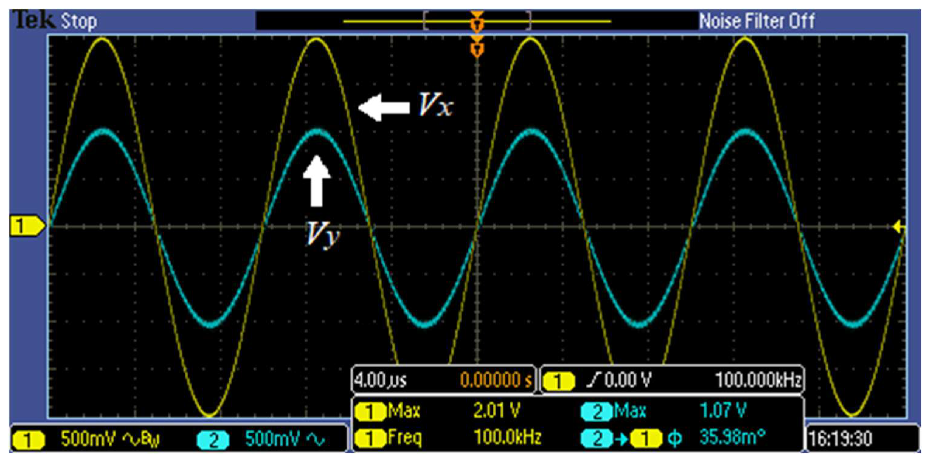
An experimental setup has been designed with the commercially available AD844 ICs to verify the operation of the proposed negative lossless GCM. The capacitance cancellation circuit is shown in Figure 17. Supply voltages of ±15 V were selected. The experimental results have been obtained out by selecting Ra = Rb = 1 kΩ and Cc = 1 nF. By choosing the passive components of the proposed GCM to eliminate the parasitic capacitor, Cc = 1 nF, R1 = 10 kΩ, R2 = 10 kΩ, R3 = 100 Ω, R4 = 1 kΩ and C = 100 pF, K = −10 and Ceq = −1 nF were obtained. A sinusoidal input voltage (Vx) with an amplitude of 2 V at frequencies of 1 kHz, 10 kHz and 100 kHz was applied to the input of the circuit. The input voltage (Vx) and the voltage waveforms of the compensated capacitor (Vy) are shown in Figure 18, Figure 19 and Figure 20. According to the test results, it can be seen that the voltages Vx and Vy are approximately in the same phase. The phase difference between the voltages was measured as 2.2° at most. As a result, the effect of the parasitic capacitor Cc is compensated for by the proposed GCM. Since the resistances Ra and Rb are chosen to be equal, the circuit works as a voltage divider and the voltage Vy is approximately half of the voltage Vx.
7. Conclusions
In this study, a new circuit configuration was introduced to realize the negative lossless GCM. The proposed circuit contains a single CFOA, four resistors, and a grounded capacitor. A detailed analysis of the circuit has been carried out. The factors affecting the frequency range have been investigated through mathematical analyses. In order to reduce the power consumption of the circuit, a CFOA was obtained by using DTMOS transistors. The simulation results were obtained with the SPICE program using 0.13 µm IBM CMOS technology parameters. The total power consumption of the circuit was 1.6 mW. The workability of the circuit has been shown by providing a capacitive cancellation circuit application and an experimental study.
Author Contributions
Conceptualization of this manuscript was by M.V.; the methodology by M.V., E.Ö. and F.K.; software verifications in SPICE by M.V.; validation by M.V., E.Ö. and F.K.; formal checking of the analysis by E.Ö. and F.K.; investigation by M.V.; resources by M.V., E.Ö. and F.K.; data curation by M.V.; writing—original draft preparation by M.V.; writing—review and editing by M.V., E.Ö. and F.K.; visualization by M.V.; supervision by E.Ö. and F.K.; project administration by M.V., E.Ö. and F.K. All authors have read and agreed to the published version of the manuscript.
Funding
This research received no external funding.
Data Availability Statement
The datasets generated during and/or analyzed during the current study are available from the corresponding author on reasonable request.
Conflicts of Interest
The authors declare no conflicts of interest.
References
- Ozenli, D.; Alaybeyoglu, E. An electronically tunable CMOS implementation of capacitance multiplier employing CCCDTA. AEU-Int. J. Electron. Commun. 2022, 155, 154359. [Google Scholar] [CrossRef]
- Dogan, M.; Yuce, E. A new CFOA based grounded capacitance multiplier. AEU-Int. J. Electron. Commun. 2020, 115, 153034. [Google Scholar] [CrossRef]
- Ozenli, D.; Alaybeyoglu, E.; Kuntman, H. A tunable lossy grounded capacitance multiplier circuit based on VDTA for the low frequency operations. Analog Integr. Circuits Signal Process. 2022, 113, 163–170. [Google Scholar] [CrossRef]
- Kumar, A.; Singh, D.; Nand, D. A Novel CFDITA-Based Design of Grounded Capacitance Multiplier and Its Transpose Structure. Circuits Syst. Signal Process. 2022, 41, 5319–5339. [Google Scholar] [CrossRef]
- Kumar, A.; Chaturvedi, B.; Jagga, S. New CMOS Compatible Realizations of Grounded/Floating L, C Multiplier and FDNC Simulators. Circuits Syst. Signal Process. 2022, 42, 1911–1939. [Google Scholar] [CrossRef]
- Yucehan, T.; Yuce, E. A New Grounded Capacitance Multiplier Using a Single ICFOA and a Grounded Capacitor. IEEE Trans. Circuits Syst. II Express Briefs 2022, 69, 729–733. [Google Scholar] [CrossRef]
- Tangsrirat, W.; Channumsin, O.; Pimpol, J. Electronically adjustable capacitance multiplier circuit with a single Voltage Differencing Gain Amplifier (VDGA). Inf. MIDEM 2019, 49, 211–217. [Google Scholar] [CrossRef]
- Özer, E.; Başak, M.E.; Kaçar, F. Realizations of lossy and lossless capacitance multiplier using CFOAs. AEU-Int. J. Electron. Commun. 2020, 127, 153444. [Google Scholar] [CrossRef]
- Khan, I.A.; Ahmed, M.T. Ota-based integrable voltage/current-controlled ideal c-multiplier. Electron. Lett. 1986, 22, 365–366. [Google Scholar] [CrossRef]
- Biolek, D.; Vavra, J.; Keskin, A.Ü. CDTA-based capacitance multipliers. Circuits Syst. Signal Process. 2019, 38, 1466–1481. [Google Scholar] [CrossRef]
- Lahiri, A. DO-CCII based generalised impedance convertor simulates floating inductance, capacitance multiplier and FDNR. Aust. J. Electr. Electron. Eng. 2010, 7, 15–20. [Google Scholar] [CrossRef]
- Minaei, S.; Yuce, E.; Cicekoglu, O. A versatile active circuit for realising floating inductance, capacitance, FDNR and admittance converter. Analog Integr. Circuits Signal Process. 2006, 47, 199–202. [Google Scholar] [CrossRef]
- Abuelma’Atti, M.T.; Tasadduq, N.A. Electronically tunable capacitance multiplier and frequency-dependent negative-resistance simulator using the current-controlled current conveyor. Microelectron. J. 1999, 30, 869–873. [Google Scholar] [CrossRef]
- Saad, R.A.; Soliman, A.M. On the systematic synthesis of CCII-based floating simulators. Int. J. Circuit Theory Appl. 2010, 38, 935–967. [Google Scholar] [CrossRef]
- Yuce, E. Floating inductance, FDNR and capacitance simulation circuit employing only grounded passive elements. Int. J. Electron. 2006, 93, 679–688. [Google Scholar] [CrossRef]
- Yuce, E. A novel floating simulation topology composed of only grounded passive components. Int. J. Electron. 2010, 97, 249–262. [Google Scholar] [CrossRef]
- Yuce, E.; Minaei, S. On the realization of simulated inductors with reduced parasitic impedance effects. Circuits Syst. Signal Process. 2009, 28, 451–465. [Google Scholar] [CrossRef]
- Yuce, E.; Minaei, S.; Cicekoglu, O. Resistorless floating immittance function simulators employing current controlled conveyors and a grounded capacitor. Electr. Eng. 2006, 88, 519–525. [Google Scholar] [CrossRef]
- Lahiri, A.; Gupta, M. Realizations of grounded negative capacitance using CFOAs. Circuits Syst. Signal Process. 2011, 30, 143–155. [Google Scholar] [CrossRef]
- Abuelma’atti, M.T.; Dhar, S.K. New CFOA-based floating immittance emulators. Int. J. Electron. 2016, 103, 1984–1997. [Google Scholar] [CrossRef]
- Dogan, M.; Yuce, E. Supplementary single active device based grounded immittance function simulators. AEU-Int. J. Electron. Commun. 2018, 94, 311–321. [Google Scholar] [CrossRef]
- Al-Absi, M.A.; Al-Khulaifi, A. A Novel Tunable Grounded Positive and Negative Impedance Multiplier. IEEE Trans. Circuits Syst. Express Briefs 2019, 66, 924–927. [Google Scholar] [CrossRef]
- Stornelli, V.; Safari, L.; Barile, G.; Ferri, G. A New Extremely Low Power Temperature Insensitive Electronically Tunable VCII-Based Grounded Capacitance Multiplier. IEEE Trans. Circuits Syst. II Express Briefs 2021, 68, 72–76. [Google Scholar] [CrossRef]
- Stornelli, V.; Safari, L.; Barile, G.; Ferri, G. A new VCII based grounded positive/negative capacitance multiplier. AEU-Int. J. Electron. Commun. 2021, 137, 153793. [Google Scholar] [CrossRef]
- Özer, E. Electronically tunable CFTA based positive and negative grounded capacitance multipliers. AEU-Int. J. Electron. Commun. 2021, 134, 153685. [Google Scholar] [CrossRef]
- Başak, M.E.; Özer, E. Electronically tunable grounded inductance simulators and capacitor multipliers realization by using single Current Follower Transconductance Amplifier (CFTA). Analog Integr. Circuits Signal Process. 2022, 112, 401–415. [Google Scholar] [CrossRef]
- Ferri, G.; Safari, L.; Barile, G.; Scarsella, M.; Stornelli, V. New Resistor-Less Electronically Controllable ±C Simulator Employing VCII, DVCC, and a Grounded Capacitor. Electronics 2022, 11, 286. [Google Scholar] [CrossRef]
- Bhaskar, D.R.; Mann, G.; Kumar, P. OTRA-based positive/negative grounded capacitance multiplier. Analog Integr. Circuits Signal Process. 2022, 111, 469–481. [Google Scholar] [CrossRef]
- Petrović, P.B. Single VDTA-based Lossless and Lossy Electronically Tunable Positive and Negative Grounded Capacitance Multipliers. Circuits Syst. Signal Process. 2022, 41, 6581–6614. [Google Scholar] [CrossRef]
- Shrivastava, M.; Kumar, P.; Bhaskar, D.R. Negative Capacitance Multiplier Configuration Using Single CFOA Employing Grounded Capacitor. In Proceedings of the 2022 International Conference on Electrical, Computer, Communications and Mechatronics Engineering (ICECCME), Maldives, 16–18 November 2022; pp. 1–4. [Google Scholar] [CrossRef]
- Raj, A.; Bhaskar, D.R.; Shrivastava, M.; Kumar, P. New negative-grounded capacitance multiplier circuits. Int. J. Circuit Theory Appl. 2023, 51, 1476–1491. [Google Scholar] [CrossRef]
- Analog Devices AD844 60 MHz, 2000 V/μs, Monolithic Op Amp with Quad Low Noise. 2017. Available online: https://www.analog.com/media/en/technical-documentation/data-sheets/ad844.pdf (accessed on 1 December 2023).
- Özer, E. A DTMOS based Four-Quadrant Analog Multiplier. Electrica 2020, 20, 207–217. [Google Scholar] [CrossRef]
- Başak, M.E.; Özer, E.; Kaçar, F.; Özenli, D. DTMOS Based High Bandwidth Four-Quadrant Analog Multiplier. Inf. Midem 2020, 50, 137–146. [Google Scholar] [CrossRef]
- Özer, E.; Başak, M.E.; Kaçar, F. A four-quadrant analog multiplier using DTMOS for low power applications. Int. J. Electron. 2022, 110, 753–767. [Google Scholar] [CrossRef]
- Yildirim, M. Design of low-voltage and low-power current-mode DTMOS transistor based full-wave/half-wave rectifier. Analog Integr. Circuits Signal Process. 2021, 106, 459–465. [Google Scholar] [CrossRef]
- Konal, M.; Kacar, F. DTMOS based low-voltage low-power all-pass filter. Analog Integr. Circuits Signal Process. 2021, 108, 173–179. [Google Scholar] [CrossRef]
- Hassanein, W.S.; Awad, I.A.; Soliman, A.M. New high accuracy CMOS current conveyors. AEU-Int. J. Electron. Commun. 2005, 59, 384–391. [Google Scholar] [CrossRef]
- Başak, M.E. Realization of DTMOS based CFTA and multiple input single output biquadratic filter application. AEU-Int. J. Electron. Commun. 2019, 106, 57–66. [Google Scholar] [CrossRef]
Figure 1.
Circuit symbol of the CFOA.

Figure 2.
Equivalent circuit of the CFOA.

Figure 3.
The proposed negative lossless grounded capacitance multiplier.

Figure 4.
Parasitic impedances of the CFOA.

Figure 5.
Equivalent circuit taking into account the non-ideal gains of the CFOA.

Figure 6.
DTMOS transistor and its circuit symbol [39].
Figure 6.
DTMOS transistor and its circuit symbol [39].

Figure 7.
Internal structure of the CFOA using DTMOS transistors [8].
Figure 7.
Internal structure of the CFOA using DTMOS transistors [8].

Figure 8.
Frequency response of the proposed negative lossless GCM and ideal capacitor for K = −10, −50.5, and −500.5 by selecting C = 100 pF; (a) magnitude and (b) phase responses.
Figure 8.
Frequency response of the proposed negative lossless GCM and ideal capacitor for K = −10, −50.5, and −500.5 by selecting C = 100 pF; (a) magnitude and (b) phase responses.

Figure 9.
Frequency response of the proposed negative lossless GCM and ideal capacitor for Ceq = −5, −50, and −500 nF by selecting K = 10, C1 = 0.5, 5, and 50 nF; (a) magnitude and (b) phase responses.
Figure 9.
Frequency response of the proposed negative lossless GCM and ideal capacitor for Ceq = −5, −50, and −500 nF by selecting K = 10, C1 = 0.5, 5, and 50 nF; (a) magnitude and (b) phase responses.

Figure 10.
Frequency responses of the proposed negative lossless GCM for various supply voltages; (a) magnitude and (b) phase responses.
Figure 10.
Frequency responses of the proposed negative lossless GCM for various supply voltages; (a) magnitude and (b) phase responses.

Figure 11.
Monte Carlo simulation results for 10% variation in the threshold voltages (VTH) and gate oxide thickness (tox) of all the MOS transistors; (a) magnitude and (b) phase responses.
Figure 11.
Monte Carlo simulation results for 10% variation in the threshold voltages (VTH) and gate oxide thickness (tox) of all the MOS transistors; (a) magnitude and (b) phase responses.

Figure 12.
Monte Carlo simulation results for 5% variation in width of all the MOS transistors; (a) magnitude and (b) phase responses.
Figure 12.
Monte Carlo simulation results for 5% variation in width of all the MOS transistors; (a) magnitude and (b) phase responses.

Figure 13.
Temperature analysis for the proposed negative lossless GCM; (a) magnitude and (b) phase responses.
Figure 13.
Temperature analysis for the proposed negative lossless GCM; (a) magnitude and (b) phase responses.


Figure 15.
Frequency performance of the capacitance cancellation circuit.

Figure 16.
The current waveforms of and for the circuit in Figure 14.
Figure 16.
The current waveforms of and for the circuit in Figure 14.

Figure 17.
Experimental setup.

Figure 18.
Vx and Vy voltage waveforms at f = 1 kHz.

Figure 19.
Vx and Vy voltage waveforms at f = 10 kHz.

Figure 20.
Vx and Vy voltage waveforms at f = 100 kHz.

Table 1.
The transistor dimensions.
| Transistors | W (μm)/L (μm) |
|---|---|
| M1–M13 | 130/0.65 |
| M14, M15, M20–M23, M25, M26, M28 | 13/0.65 |
| M24, M27 | 26/0.65 |
| M16–M19 | 15.6/0.26 |
Table 2.
Parasitic impedances and non-ideal gains of the CFOA.
| Parasitic Impedances | Values |
|---|---|
| RX | 0.637 Ω |
| RW | 0.637 Ω |
| RZ | 20.04 kΩ |
| CZ | 66 fF |
| CY | 8.23 fF |
| α | 0.999972 |
| β | 1.000009 |
| η | 1.000009 |
Table 4.
Comparison of negative CM circuit.
| References | # and Type of ABB | # of Resistors | # of Capacitors | Electronic Tuning | Multiplication n Factor | Matching Condition | Technology | Operation Frequency | Power Dissipation | ||
|---|---|---|---|---|---|---|---|---|---|---|---|
| F | G | F | G | ||||||||
| [19] in Figure 2 | 2 CFOA | 0 | 2 | 0 | 1 | No | 0.5 | No | 0.35 µm | NA | NA |
| [19] in Figure 3 | 2 CFOA | 0 | 2 | 0 | 1 | No | 0.5 | No | 0.35 µm | NA | NA |
| [19] in Figure 4 | 1 CFOA | 1 | 1 | 1 | 0 | No | 0.5 | No | 0.35 µm | 1 kHz to 5 MHz | NA |
| [19] in Figure 5 | 1 CFOA | 2 | 0 | 0 | 1 | No | 0.5 | No | 0.35 µm | NA | NA |
| [20] in Figure 1d | 2 CFOA | 2 | 0 | 1 | 0 | No | NA | No | AD844 | NA | NA |
| [21] in Figure 8 | 1 CFOA | 1 | 2 | 0 | 1 | No | NA | Yes | 0.13 µm | NA | NA |
| [22] in Figure 11 | 1 CFOA, 2 OTA | 0 | 0 | 0 | 1 | Yes | NA | No | AD844, LM13700N | 2 Hz to 7 MHz | NA |
| [23] in Figure 1b | 1 EVCII− | 0 | 0 | 1 | 0 | Yes | 100 | No | 0.18 µm | 80 Hz to 40 kHz | 67 nW |
| [24] in Figure 4 | 2 VCII+ | 1 | 1 | 1 | 0 | No | 50 | No | 0.35 µm | 10 MHz | 1.5 mW |
| [25] in Figure 6 | 2 CFTA | 0 | 2 | 1 | 0 | Yes | 20.3 | No | 0.13 µm | 10 kHz to 100 MHz | NA |
| [25] in Figure 7 | 2 CFTA | 0 | 2 | 1 | 0 | Yes | 20.3 | No | 0.13 µm | 10 kHz to 100 MHz | NA |
| [26] in Figure 7 | 1 CFTA | 0 | 1 | 1 | 0 | Yes | 10 | No | 0.18 µm | 280 Hz to 4.15 MHz | NA |
| [27] in Figure 2 | 1 VCII ±, 1 E-DVCC | 0 | 0 | 0 | 1 | Yes | 25.4 | No | 0.18 µm | 10 kHz to 1 MHz | 3.184 mW |
| [28] in Figure 2 | 1 OTRA, 1 VF | 3 | 0 | 1 | 0 | Yes | 99 | Yes | 0.18 µm | 100 Hz to 1 MHz | NA |
| [29] in Figure 1 | 1 VDTA | 0 | 1 | 1 | 0 | Yes | 20 | No | 0.18 μm | 100 Hz to 100 MHz | 0.89 mW |
| [30] in Figure 1 | 1 CFOA | 3 | 0 | 1 | 0 | No | 26 | No | AD844 | 1 kHz to 100 kHz | NA |
| [31] in Figure 2a | 1 CFOA | 2 | 0 | 0 | 1 | No | 2001 | No | AD844 | 4 kHz to 1 MHz | NA |
| [31] in Figure 2b | 1 CFOA | 2 | 0 | 0 | 1 | Yes | 201 | No | AD844 | 4 kHz to 1 MHz | NA |
| [31] in Figure 2c | 1 CFOA | 2 | 0 | 0 | 1 | No | 400 | No | AD844 | 4 kHz to 1 MHz | NA |
| Proposed | 1 CFOA | 2 | 2 | 0 | 1 | Yes | 500.5 | Yes | 0.13 µm | 8 Hz to 80 MHz | 1.6 mW |
Abbreviations: ABB: active building block; CFOA: current feedback operational amplifier; CFTA: current follower transconductance amplifier; E-DVCC: electronically tunable differential voltage current conveyor; F: floating; G: grounded; NA: not available; OTA: operational transconductance amplifier; VCII: second generation voltage conveyor; VF: voltage follower.
Disclaimer/Publisher’s Note: The statements, opinions and data contained in all publications are solely those of the individual author(s) and contributor(s) and not of MDPI and/or the editor(s). MDPI and/or the editor(s) disclaim responsibility for any injury to people or property resulting from any ideas, methods, instructions or products referred to in the content. |
© 2024 by the authors. Licensee MDPI, Basel, Switzerland. This article is an open access article distributed under the terms and conditions of the Creative Commons Attribution (CC BY) license (https://creativecommons.org/licenses/by/4.0/).
Share and Cite
MDPI and ACS Style
Vahbeh, M.; Özer, E.; Kaçar, F. Design of Lossless Negative Capacitance Multiplier Employing a Single Active Element. Electronics 2024, 13, 1163. https://doi.org/10.3390/electronics13061163
AMA Style
Vahbeh M, Özer E, Kaçar F. Design of Lossless Negative Capacitance Multiplier Employing a Single Active Element. Electronics. 2024; 13(6):1163. https://doi.org/10.3390/electronics13061163
Chicago/Turabian StyleVahbeh, Mutasem, Emre Özer, and Fırat Kaçar. 2024. "Design of Lossless Negative Capacitance Multiplier Employing a Single Active Element" Electronics 13, no. 6: 1163. https://doi.org/10.3390/electronics13061163
Note that from the first issue of 2016, this journal uses article numbers instead of page numbers. See further details here.