Article

A Two-Stage Sub-Threshold Voltage Reference Generator Using Body Bias Curvature Compensation for Improved Temperature Coefficient

1
Department of Electrical Engineering, Sensors and Interfaces Research Group, University of Isfahan, Isfahan 8174673441, Iran
2
Department of Electronics and Telecommunications (DET), Politecnico di Torino, 10129 Torino, Italy
*
Authors to whom correspondence should be addressed.
Electronics 2024, 13(7), 1390; https://doi.org/10.3390/electronics13071390
Submission received: 4 March 2024 / Revised: 1 April 2024 / Accepted: 2 April 2024 / Published: 7 April 2024

Abstract

:
Leakage diodes cause deviations in the thermal drift of ultra-low-power two-transistor (2T) reference circuits, resulting in either convex or concave output voltages against temperature, depending on the reference transistor types (n-type/p-type). This paper investigates the combined application of the convexity and concavity properties exhibited by the output voltage of complementary 2T references, one n-type and one p-type. By exploiting the body bias effect, this approach mitigates variations in the output reference voltage caused by temperature fluctuations. Software optimization is also used to obtain the required aspect ratios after formulating the required criteria for drain-induced barrier lowering (DIBL) elimination in the first stage. The performance of the proposed reference is evaluated by post-layout Monte Carlo simulations. In the range of 0 °C to 100 °C, the output reference voltage has an average temperature coefficient (TC) of 26.7 ppm/°C without any temperature trim. The output reference voltage is 195.5 mV with a standard deviation of 13.6 mV. The line sensitivity (LS) is 17.1 ppm/V in the supply voltage range of 0.5 V to 2.1 V at 25 °C. At 25 °C and 0.5 V, the power consumption is 28.8 pW, increasing to a maximum of 1.3 nW at 100 °C and 2.1 V.

1. Introduction

For proper operation, an accurate voltage or current reference [1] is needed in most electronic systems. In particular, it is a fundamental block of amplifiers [2], analog-to-digital converters (ADCs) [3], and regulators [4], among others. A voltage or current reference should be independent of temperature and supply voltage and should be robust against variations in the fabrication process. Moreover, since reference circuits are always on, their power consumption is particularly critical in the Internet of Things (IoT) sensor nodes, wearables, and medical implants. Ultra-low-power (ULP) references in mainstream CMOS technology have been actively investigated in recent years, lowering the power budget down to a few hundred femtowatts [5,6].
In ULP references, resistors are problematic because they occupy more silicon areas at low currents. Large resistors can be replaced by the transistor gate leakage current [7] or by MOSFET-only topologies. In such ULP CMOS voltage references (CVRs), however, the output is typically related to the transistors’ threshold [8,9,10,11,12], which can be significantly affected by process variations. In order to enhance the robustness of CVRs to process variations, proportional to the faster-skewed process (PTFP) and complementary to the faster-skewed process (CTFP), circuits have been combined as part of the hybrid architecture presented in [13]. However, the minimum supply voltage and its TC are not very competitive. In [14], body biasing is exploited to design a reference less sensitive to the threshold voltage variations. However, it requires a minimum supply of 1.2 V and has a TC ranging from 48 ppm/°C to 124 ppm/°C. Body biasing has also been used to adjust the output voltage at the expense of large power consumption and TC [15].
In this context, lowering the TC is one of the main challenges of ULP CVRs operating in the subthreshold region. In [16], it is shown that the pMOS diode’s leakage current can be used to enhance the temperature behavior of the output reference voltage in ultra-low-power CVRs.
Adjusting the curvature of the reference voltage-to-temperature characteristic is a prevalent method employed in Bandgap Voltage References (BGRs) to enhance TC performance. For instance, in [17], the adjusted-temperature-curvature (ATC) compensation circuit is used to lower the TC down to 1.67 ppm/°C. However, the minimum supply voltage of 1.3 V and power consumption of 36.4 µW are incompatible with the ULP design target.
Various techniques to improve the LS have been presented in the literature regarding the sensitivity to supply voltage changes. Using a quasi-cascode current mirror, the authors of [18] reduced the LS of [19] from 0.44%/V to 0.065%/V. This improvement was made possible at the cost of raising the supply voltage and power consumption from 0.45 V and 2.6 nW to 0.7 V and 25.9 nW, respectively.
The introduction of a two-stage circuit is another way to enhance LS [11]. In such references, the supply voltage primarily affects the reference voltage via the DIBL effect. To counteract the DIBL effect, a current proportional to the supply voltage is subtracted from the bias current of the output reference voltage branch [12]. This approach improves the LS from 1100 ppm/V to 190 ppm/V. By combining a two-stage structure with a DIBL compensator, the voltage reference circuit presented in [20] achieves an LS of 143.8 ppm/V. The LS and TC corrections are carried out in the structure’s first and second stages, respectively. However, the curvature of the output voltage versus temperature characteristics in [20] cannot be altered because all transistors in the second stage are nMOS.
This paper presents a new TC correction circuit as the second stage in [20]. In detail, 2T voltage references of the p-type and the n-type are combined in this structure to reduce the temperature changes in the output reference voltage. In the output voltage-to-temperature characteristics of a 2T n-type voltage reference, a leakage current drawn by reverse-biased diodes at the output node produces a concave curve. In contrast, the leakage current sourced by reverse-biased diodes produces a convex characteristic in the 2T p-type voltage reference [16]. In the proposed reference, the two opposite behaviors of concavity and convexity of the n-type and p-type references are compensated by biasing the body of the load transistor in a 2T p-type reference with the output voltage of an n-type reference. Moreover, the LS is also improved by optimizing the DIBL effect removal in the first stage.
In the rest of this paper, the two-stage structure of [20] will be reviewed, and a more accurate expression for the DIBL compensation approach will be introduced in Section 2. Section 3 presents the proposed voltage reference, while the optimization of its TC by the new technique is given in Section 4. Section 5 reports the results from post-layout simulations of the proposed voltage reference circuit, and finally, some concluding results are drawn in Section 6.

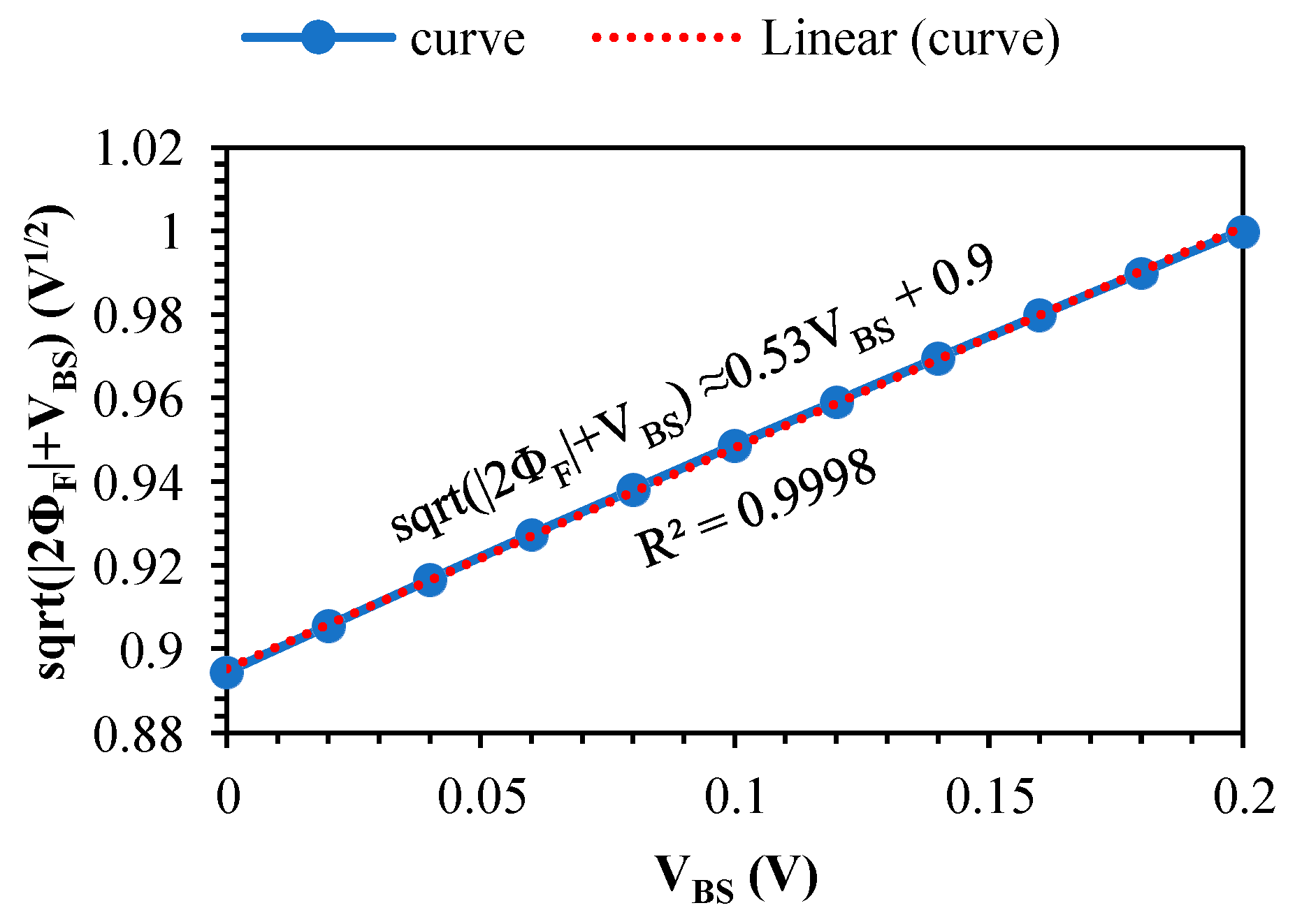
2. Dibl Effect Compensation

This section begins with a summary of the DIBL effect compensation and LS improvement technique presented in [20], followed by a proposed approach for optimizing DIBL effect compensation. Figure 1 shows the two-stage structure with a DIBL effect compensator introduced in [20]. In the first stage, a DIBL effect compensator is used to reduce the LS, while for the second stage, a temperature compensator is used to correct the thermal drift of the output voltage. All transistors in the first stage are nMOS, and their bodies are connected to the ground. M1, M3, and M4 are thick oxide transistors, while M2 and M5 are thin oxide transistors. The LS corrector increases the minimum supply voltage slightly (by approximately 150 mV) in exchange for a substantial reduction in the LS. The stable output voltage of the first stage makes the TC almost constant over the entire supply voltage range. The circuit operates in the subthreshold region in which the drain current can be expressed as [21]:
I D = μ C d W L V T 2 e x p | V G S | V T H n V T 1 e x p | V D S | V T
where µ, Cd, W, and L are the mobility of electrons or holes (depending on the transistor type), depletion capacitor, width, and length of the transistor, respectively. VGS, VDS, VTH, and VT are the gate-source, drain-source, threshold, and thermal voltage, respectively. Increasing the drain-source voltage beyond 150 mV allows the last term to be ignored, although the drain-source voltage dependence remains through the DIBL effect, which influences the threshold voltage.
The effect of temperature in the first stage on the output reference voltage is approximated as follows [20]:
V R E F V R E G T = c o n s t a n t × V R E G T / V R E F = L S 2 × T C 1 × V R E G a v g 0
where VREF refers to the reference output voltage, while VREG represents the output voltage of the first stage. T denotes the absolute temperature, and TC1 and LS2 are the temperature coefficient of the first stage and line sensitivity of the second stage, respectively. As a result, the first stage output voltage changes with temperature have a negligible impact on the total TC. In this design, the gate of M2 is connected to the output node to produce a current proportional to the changes in VO with respect to the supply voltage, to be sunk from the VO node itself through M1 and M3, aiming to reduce the supply sensitivity of VREG.
This paper investigates the output voltage of the first stage in more detail and fewer simplifications than [20] to cancel DIBL’s effect better. ID3 and ID5 can be obtained as described in [20]. Therefore, ID4 = ID5ID3 can be expressed as follows:
V R E G = V T H 4 + n H V T ln K R 2 exp V T H 5 n L V T K R 1 N R 1 K R 3 exp n L V T H 1 n H V T H 2 n H + n L V T H 3 + n H V R E G n H n H + n L V T
where
K R 1 = C d , L W / L 2 / C d , H W / L 1
K R 2 = C d , L ( W / L ) 5 / C d , H ( W / L ) 4
K R 3 = ( W / L ) 3 / ( W / L ) 4
N R 1 = 1 + N R 1 and N R = n H / n L . The subscript “H” denotes thick oxide transistors, whereas the subscript “L” represents thin oxide transistors. The DIBL effect’s impact on the threshold voltage can be expressed as follows:
V T H = V T H , 0 λ D V D S
where λD is the DIBL factor and VTH,0 is the threshold voltage at |VDS| = 0. Assuming the main supply voltage changes are applied to drain-source voltages of M2 and M5, the following expression can be derived by substituting (5) in (3):
V R E G = V T H 4 + n H V T ln ( K R 2 ( exp V T H 5,0 n L V T exp λ D 5 V D S 5 n L V T K R 1 N R 1 K R 3 exp λ D 2 V D S 2 n H + n L V T × exp n L V T H 1 n H V T H 2,0 n H + n L V T H 3 + n H V R E G n H n H + n L V T ) )
To compensate for DIBL’s effect, the expression in the logarithm argument should be independent of the drain-source voltages of M2 and M5. In the circuit design, transistor dimensions are chosen so that VDS2 ≈ VDS5 ≈ VDS. Also, VREG is assumed to be constant. In Figure 2, the simulation results show that the VREG and VX mean values are 348.7 mV and 349.3 mV, respectively. With these criteria, the following expression is obtained by differentiating the argument of the logarithm in (6) with respect to VDS and setting it equal to zero.
A K R 2 λ D 5 n L V T exp λ D 5 V D S n L V T = B K R 1 N R 1 K R 3 λ D 2 ( n L + n H ) V T exp n L λ D 2 V D S n H + n L V T
where A = exp V T H 5 , 0 / n L V T and B = exp n L V T H 1 n H V T H 2 , 0 n H + n L V T H 3 + n H V R E G n H n H + n L V T . Thus, to perform DIBL compensation, the following conditions should be met:
λ D 5 = N R 1 λ D 2
B N R 1 K R 1 N R 1 K R 3 λ D 2 = A K R 2 λ D 5
The appropriate length of transistors M2 and M5 (which affect λD2 and λD5) have to be chosen to satisfy Equation (8) in order to mitigate the DIBL effect. Then, (9) can be satisfied by KR1, KR2, and KR3. The minimum length for M2 is chosen to obtain the minimum suitable length of M5. Figure 3 shows the dependence of LS on L5 and W3 for L2 = 0.18 µm. The average of 100 Monte Carlo runs is used for each point. The shown dot has the lowest LS values in this figure. Based on the analysis, the values of L5 = 0.45 µm and W3 = 3.7 µm are chosen for the design.

3. Proposed Voltage Reference Generator

The proposed voltage reference generator aims to enhance the overall thermal drift of parasitic diode leakage currents. It achieves this by combining the opposite voltage versus temperature of 2T n-type and p-type voltage reference generators presented in Section 3.1. In Section 3.2, a comprehensive explanation of the methodology employed to integrate the temperature behaviors of the aforementioned structures, along with their corresponding mathematical expressions, is provided.

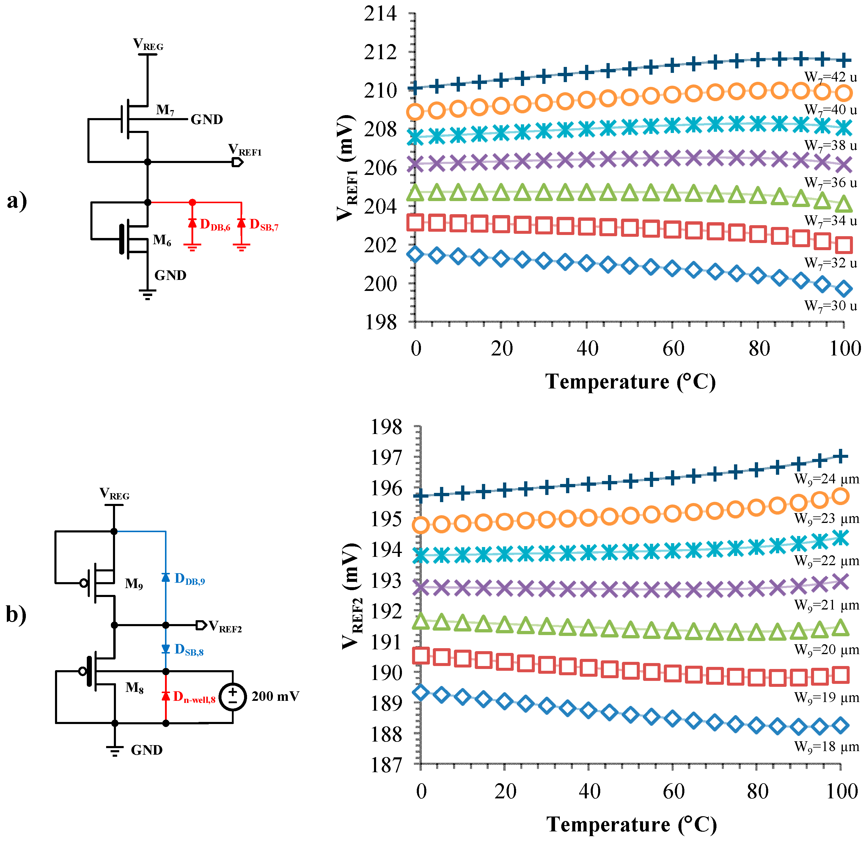
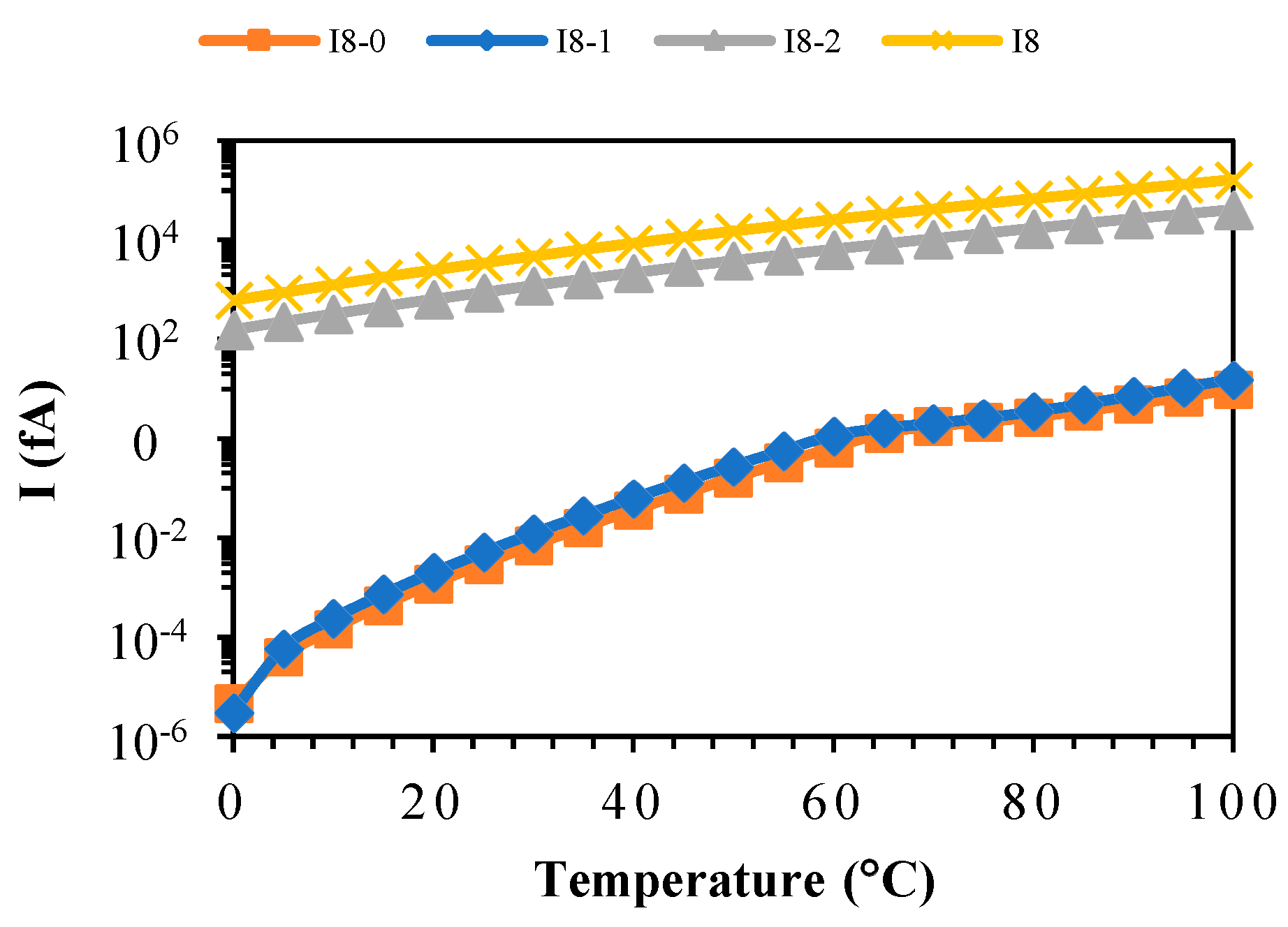
3.1. Effects of Parasitic Diodes Leakage Current in 2T n-Type and p-Type Voltage Reference Generators

Figure 4a,b illustrate the 2T n-type and p-type reference circuits, respectively. In the 2T n-type reference circuit, the output node contains two parasitic diodes, the reversed biased drain-body of M6, and the source-body of M7. Both diodes draw current from the output node and are shown in red. The reverse saturation currents drawn from the output node result in a concave reference voltage versus temperature curve for the 2T n-type reference (with the substrate connected to the ground) [16]. This behavior is illustrated in Figure 4a, which shows the simulated temperature dependence of the output voltage for different widths of the current source transistor. The length of both transistors is 2 µm, and the load transistor’s width is 20 µm.
In the 2T p-type reference, the presence of a reverse-biased junction diode between the drain-body of M9 results in the injection of a leakage current to the output node. The body terminal of M8 is biased with a 200 mV DC voltage, which resembles the approximate voltage that is to be provided by a preceding stage in the proposed design. Since the applied body potential is higher than the output voltage of this stage, the source-body diode of M8 will also inject a leakage current into the output node. The effect of the M8 n-well diode is considered as a parasitic load on the preceding stage (the preceding stage is explained in the proposed design of the following subsection), which supplies the body bias of M8. The n-well parasitic diode of M9 is located between VREG and GND and has a negligible impact on the output voltage temperature-dependent behavior; however, the leakage current of this diode will affect the power dissipation. The pull-up parasitic diodes that inject the leakage current into the output node are highlighted in blue. These parasitic diodes inject reverse saturation currents to the output node, resulting in a convex output voltage versus temperature characteristic [16], as shown in Figure 4b for different M9 transistor widths. Other dimensions are considered similar to the 2T n-type voltage reference.

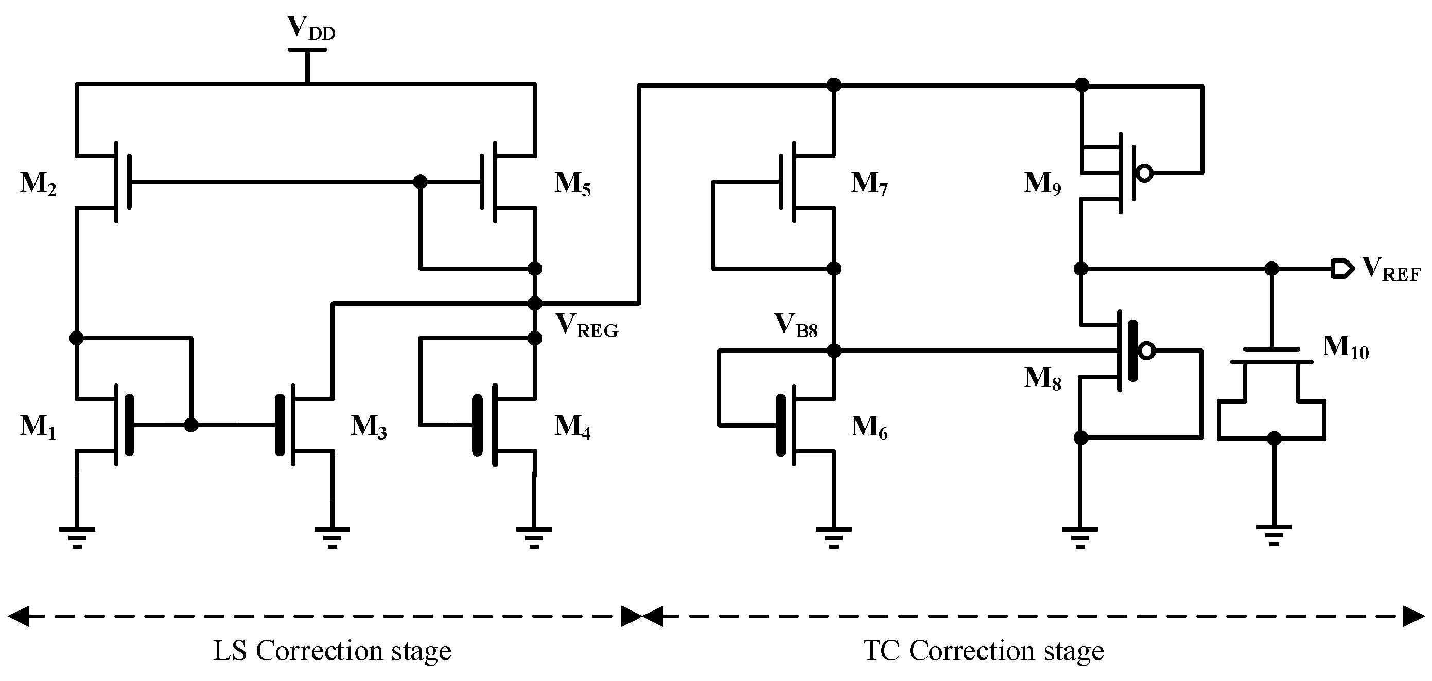
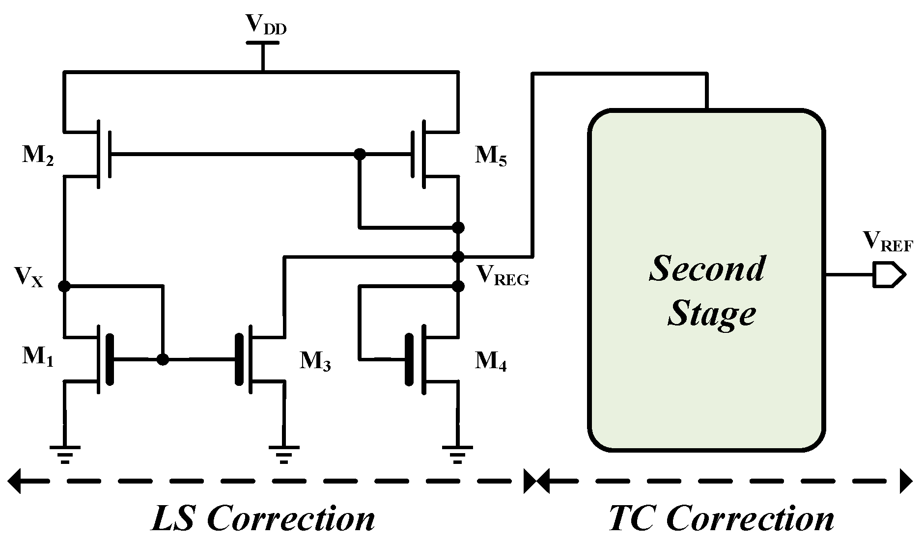
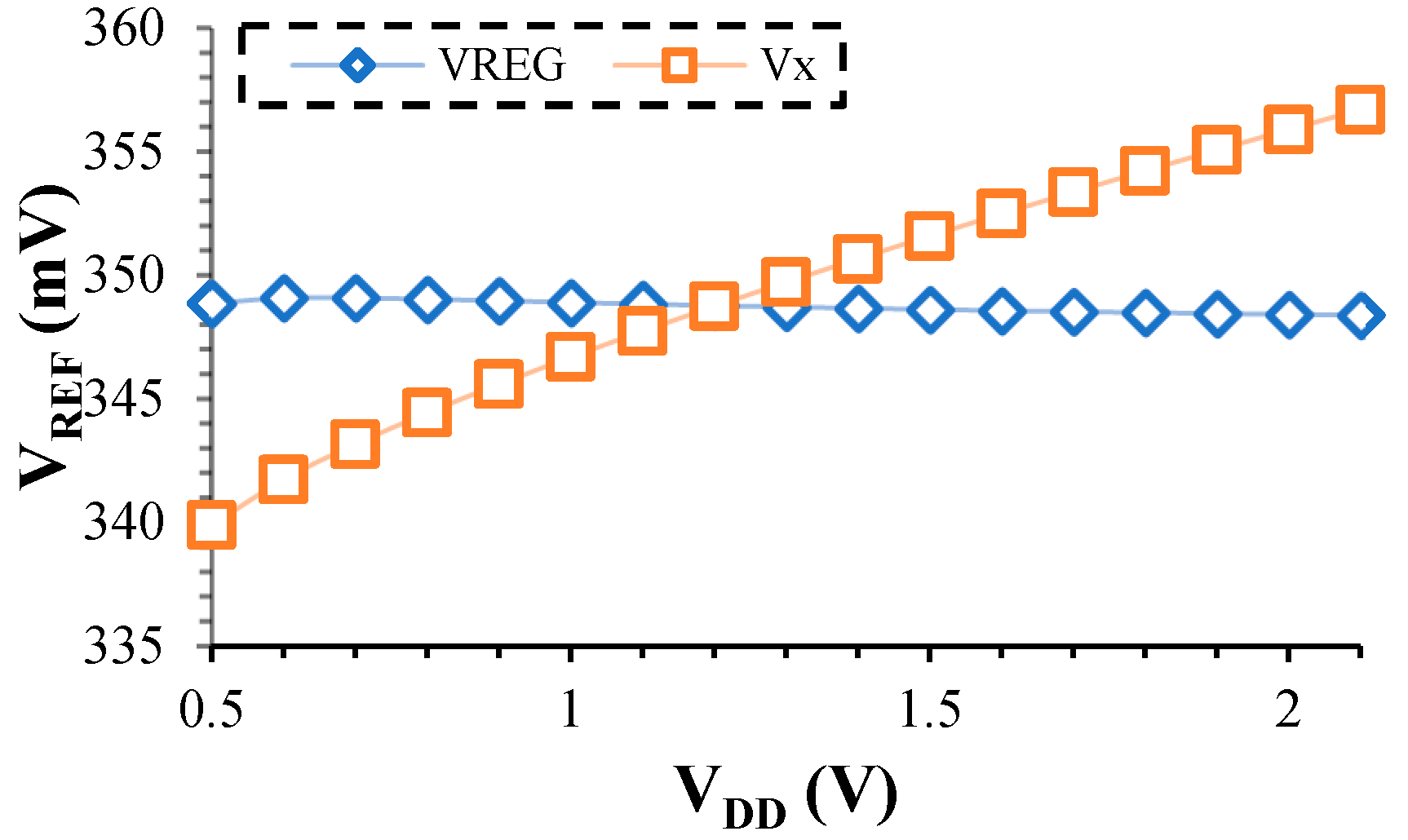
3.2. Proposed Circuit
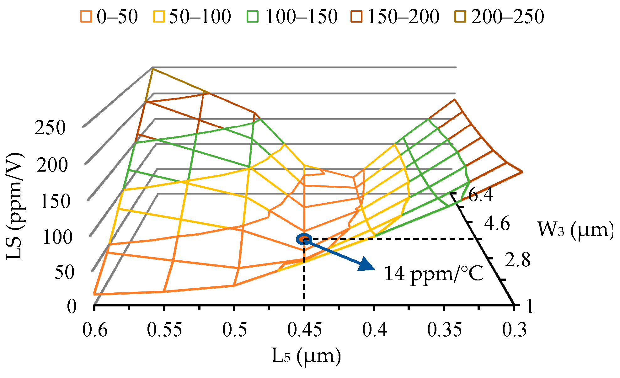
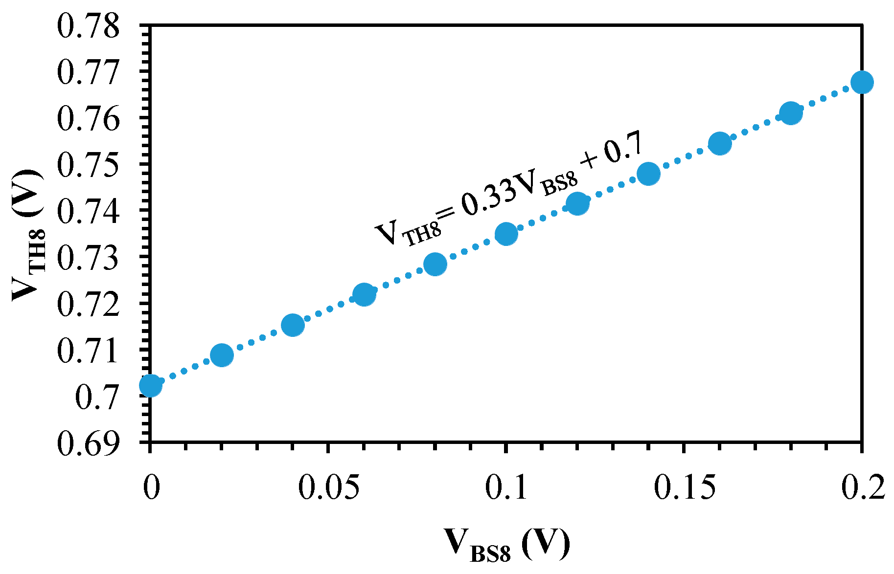
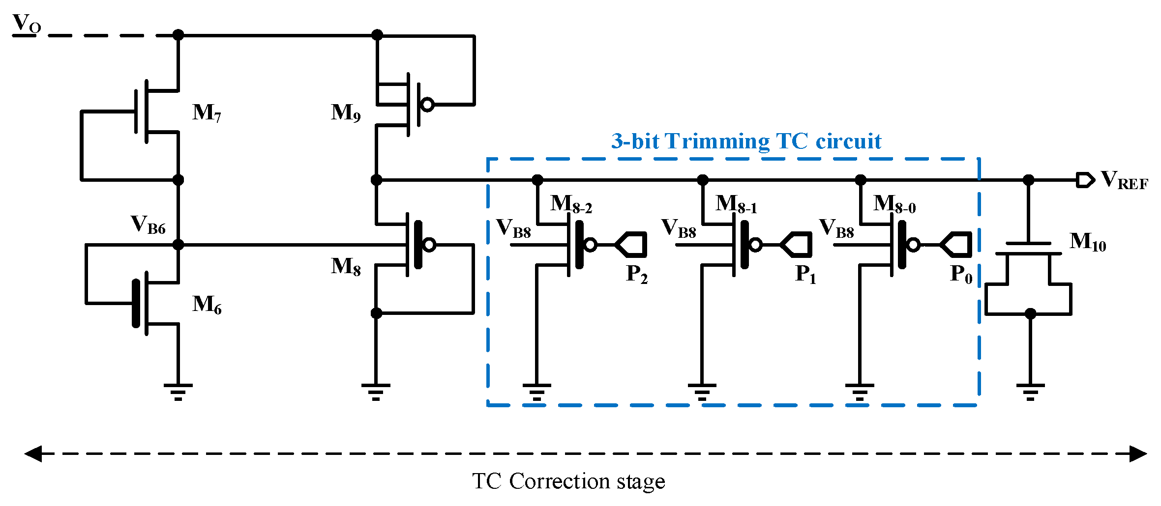
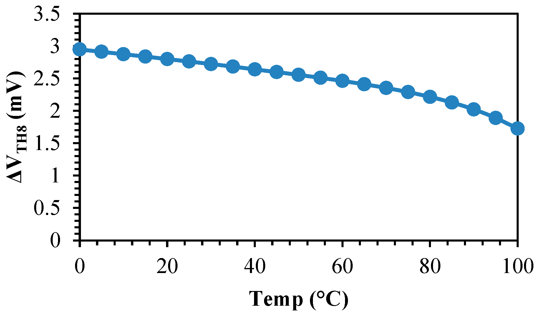
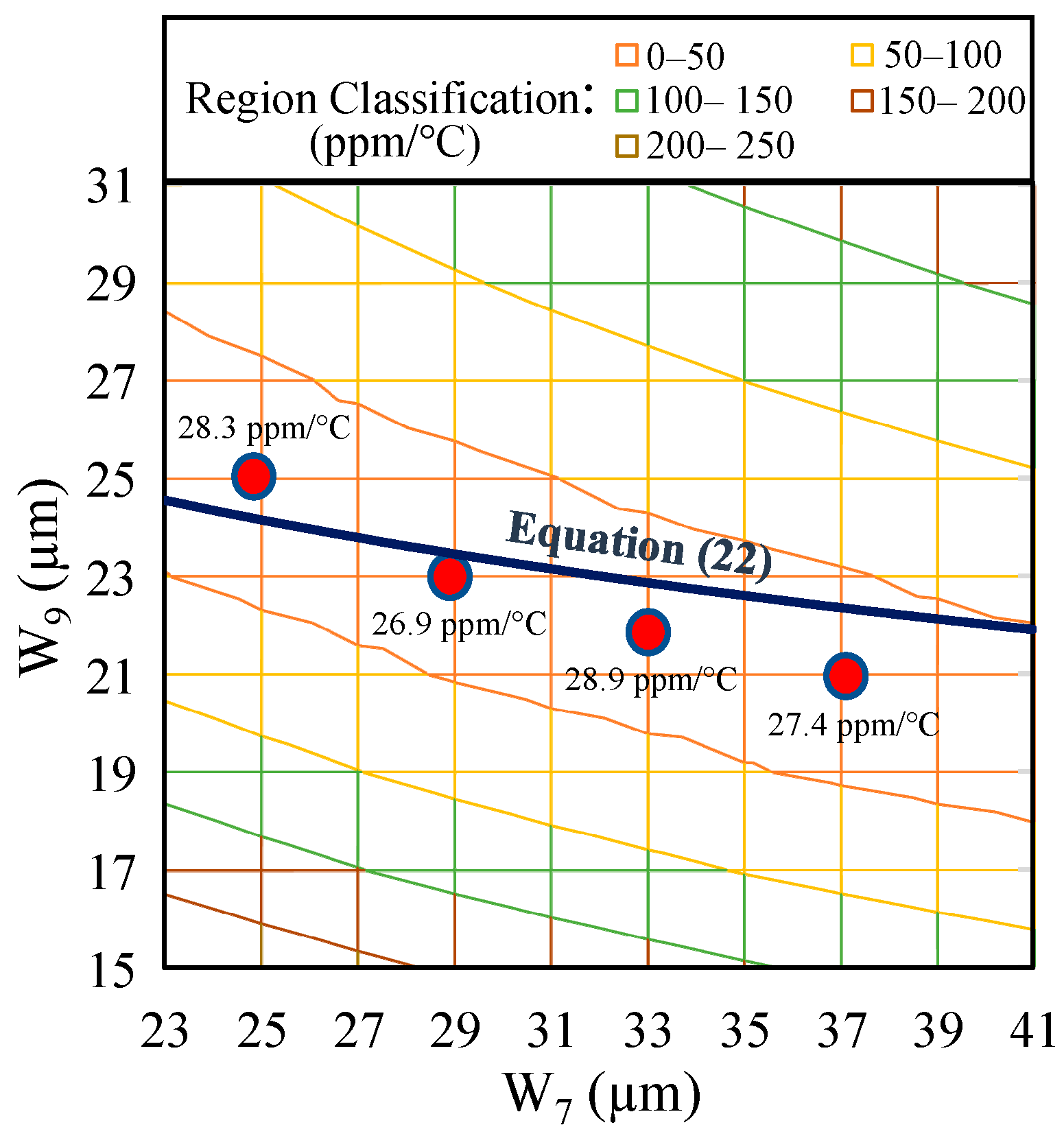
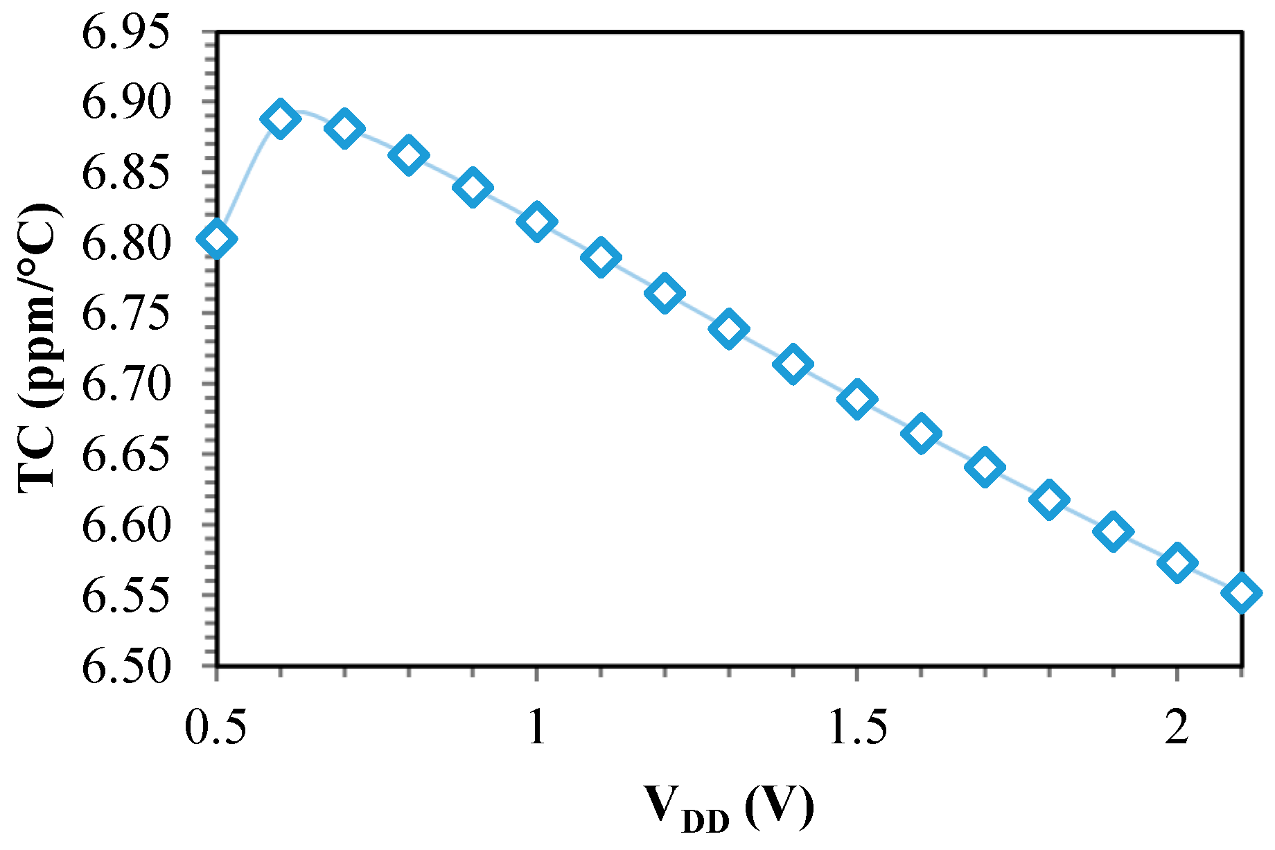
The proposed voltage reference takes advantage of the opposite concavity in the voltage versus temperature behavior of 2T n-type and p-type CVRs to achieve curvature compensation. For this purpose, the output voltage of a 2T n-type reference is used to modulate the bulk voltage of the main 2T p-type reference, as demanded, to correct the curvature of its thermal drift.
In detail, considering the dependence of the threshold voltage of a pMOS transistor on its body voltage, the following is presented:
V T H = V T H , 0 + γ 2 Φ F + V B S 2 Φ F
in which ΦF is the Fermi potential, VBS is the bulk-source voltage, and VTH,0 refers to the threshold voltage without body effect. For simplicity, 2 Φ F + V B S in (10) is linearized according to (11) as follows:
2 Φ F + V B S = C 1 V B S + C 2
|VBS| in this design is considered around 0 to 200 mV and 2ΦF ≈ 0.8 V. According to Figure 5, the C1 and C2 coefficients are approximately 0.53 and 0.9, respectively. By placing (11) into (10), C 3 = γ C 1 = 0.35 and γ C 2 2 Φ F 0 . With these coefficients, the threshold voltage is expressed by the following equation.
V T H = V T H , 0 + C 3 V B S
Equation (12) reveals that the body voltage scaled by the C3 coefficient is added to the threshold voltage. Figure 6 illustrates the variation in VTH8 versus VBS8. The slope of the variation is approximately near the predicted value of C3. Since the body of M8 is biased by a 2T n-type circuit in the proposed reference, a concave-in-temperature contribution is added to its threshold voltage. Figure 7 illustrates the difference in the threshold voltage of M8 between the zero-body-bias state and the state biased with the output voltage of the 2T n-type reference.
Imposing the equality of the drain currents of M8 and M9 and based on Equation (1), the reference voltage can be expressed as
V R E F = V T H 8 N R | V T H 9 | + n H V T ln A 1 + ln W / L 9 W / L 8
where A 1 = μ p 9 C d 9 μ p 8 C d 8 . Considering the dependence of the body terminal of M8, VBS8 = VB8VREF and also using (12) in (13), (14) is obtained.
V R E F = n H V T ln A 1 + ln W / L 9 W / L 8 1 + C 3 + V T H 8.0 N R V T H 9.0 + C 3 V B 8 1 + C 3
The value of C3 shows that VB8 will add up to the reference voltage by a factor of 0.26. By using the output voltage of 2T n-type as VB8, convexity and concavity can be adjusted to cancel each other, thus reducing the reference voltage changes. Therefore, the proposed circuit for reducing the temperature curve of the 2T p-type is shown in Figure 8.
It is possible to simplify (14) to (15).
V R E F = V R E F , 2 T P + C 3 V R E F , 2 T N 1 + C 3
VREF,2T_P and VREF,2T_N are 2T p-type and n-type reference voltages, respectively. The output reference voltage changes for VREF,2T_P and VREF,2T_N in temperature compensated form, the reference voltage obtained in (15) (through substituting VREF,2T_N and VREF,2T_P into (15)), and the reference voltage versus temperature changes are simulated in Figure 9. The mean values of VREF obtained from (15), VREF,2T_P, VREF,2T_N, and output VREF are 192.5 mV, 188.8 mV, 207.1 mV, and 195.3 mV, respectively. Assuming ID6 = ID7 and similarly to (13), VB8 is obtained as follows:
V B 8 = V T H 6 N R V T H 7 + n H V T ln A 2 + ln W / L 7 W / L 6
where A 2 = μ n 7 C d 7 μ n 6 C d 6 . Since the substrate is grounded, M7 is affected by the body effect. By substituting (12) into (16), VB8 can be expressed as follows:
V B 8 = V T H 6 , 0 N R V T H 7 , 0 + C 3 V S B 7 + n H V T ln A 2 + ln W / L 7 W / L 6
According to Figure 8 and connecting the substrate to the ground, VSB7 = VB8. Therefore, (17) can be simplified to (18).
V B 8 = n H V T ln A 2 + ln W / L 7 W / L 6 + V T H 6,0 N R V T H 7,0 1 + N R C 3
Using (18) in (14) results in the following equation:
V R E F = n H V T ln A 1 A 2 C 4 + n H V T ln W / L 9 W / L 8 · W / L 7 W / L 6 C 4 1 + C 3 + V T H 8 , 0 + C 4 V T H 6 , 0 N R V T H 9 , 0 + C 4 V T H 7 , 0 1 + C 3
where C 4 = C 3 / 1 + N R C 3 0.196 . In the first-order approximation, parameters VTH, VT, and μ are considered dependent on temperature. The threshold voltage is a complex function of temperature, which can be expressed by [22]
V T H = V T H T 0 + α T T 0 + β T T 0 2 + γ T T 0 3 +
The parameters α, β, and γ represent the first-, second-, and third-order coefficients, respectively, that describe the temperature dependence of the threshold voltage. Although this relationship is nonlinear, it can be approximated with a linear function. Additionally, using concave and convex curves for the output voltages of 2T n-type and p-type devices can help mitigate the effects of second-order nonlinearities. T0 is the reference temperature. The temperature dependence of mobility can be expressed by (21) as follows [23]:
μ T = μ T 0 T T 0 M
M is the temperature exponent of carrier mobility, which is usually 1.5. Since a ratio of the same type of mobilities is used, the thermal drift of the mobility in (19) is canceled. By substituting V T = k B T / q and using a linear function of (20) in (19), the appropriate aspect ratio is obtained to compensate for temperature dependences as follows:
W / L 9 W / L 8 · W / L 7 W / L 6 C 4 = 1 A 1 A 2 C 4 exp q n H k B α 8 + C 4 α 6 N R α 9 + C 4 α 7
By choosing suitable transistor dimensions to achieve complete temperature compensation of voltage reference and by inserting (22) into (19), a temperature-compensated expression for the output reference voltage can be obtained as follows:
V R E F = V T H + α · T 0 1 + C 3
where
V T H = V T H 8 , 0 ( T 0 ) + C 4 V T H 6 , 0 ( T 0 ) N R ( V T H 9 , 0 ( T 0 ) + C 4 V T H 7 , 0 ( T 0 )
α = N R ( α 9 + C 4 α 7 ) ( α 8 + C 4 α 6 )

4. TC Optimization

In Equation (22), the aspect ratio for temperature compensation is evaluated. The aspect ratio on the left side of the equation becomes 1.26 using the typical corner technology parameters in (22). This aspect ratio is shifted with the change in the technology parameters in various corners. Therefore, Monte Carlo analysis optimization would be more appropriate than just one corner optimization to reduce the average TC [16].
Flicker noise and short channel effects are reduced as transistor length increases [24]. To make a compromise between the occupied chip area and second-order effects, the second-stage transistor lengths are chosen at 2 µm. Figure 10 shows the Monte Carlo analysis used on the schematic to find an optimal aspect ratio for temperature compensation.
For temperature compensation, transistor widths of M6–M9 are important since the second stage is responsible for temperature correction of the output voltage. For this purpose, by selecting W6 = W8 = 20 µm, W7 and W9 are swept to find the suitable design solution. The dots represent the values of TC, as determined by post-layout Monte Carlo analysis, in the range with the lowest TC. It is noteworthy that Equation (22) reasonably estimates the optimal dimension ratio, validating the derived equations. Because of the different parameters in different corners and simplified equations, there is a slight difference between optimal dimensions based on Monte Carlo and (22). As can be seen, the optimal TC lies in W7 = 29 µm and W9 = 23 µm, which results in a TC of 26.9 ppm/°C. The dimensions of all the proposed voltage reference transistors are reported in Table 1.

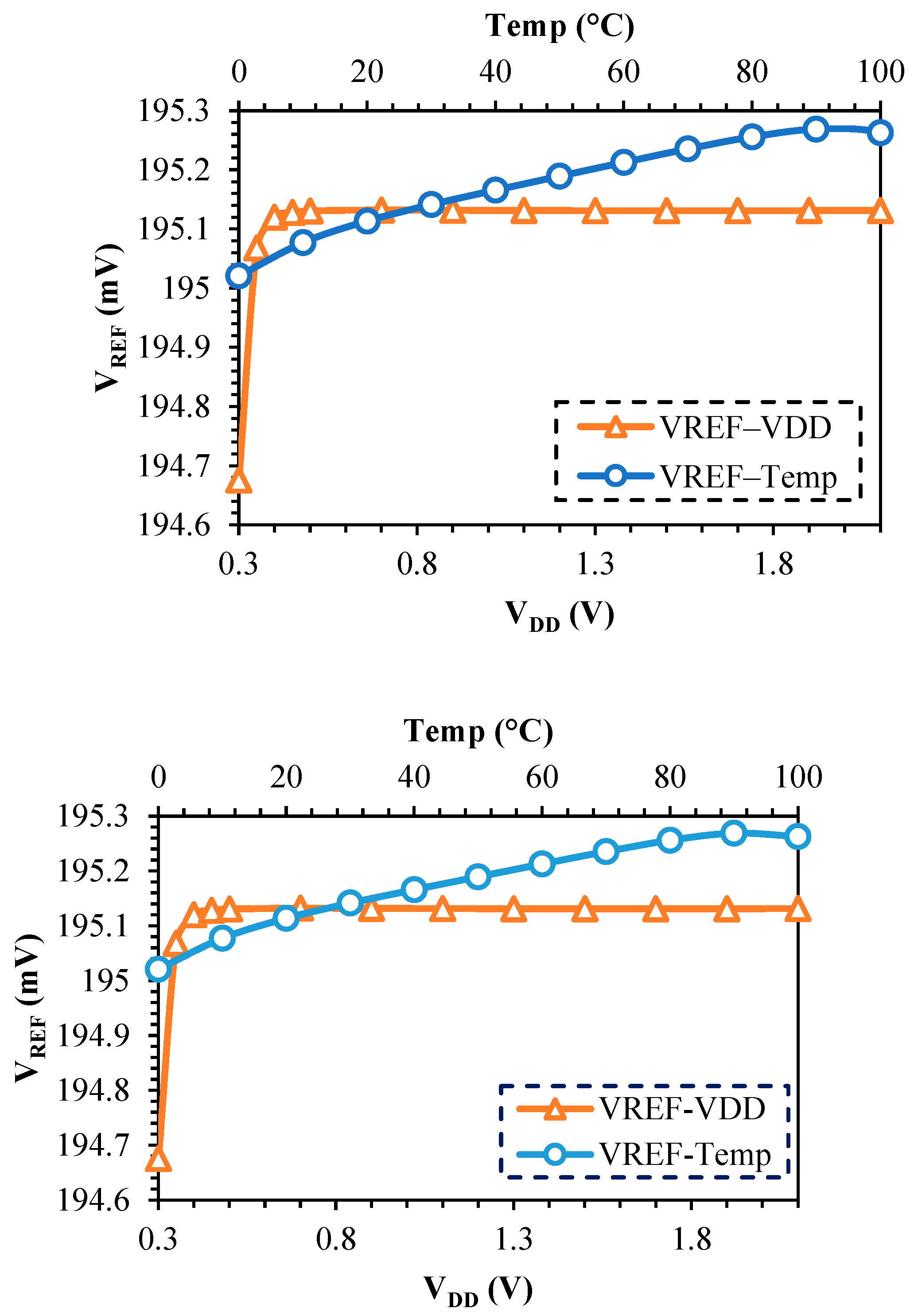
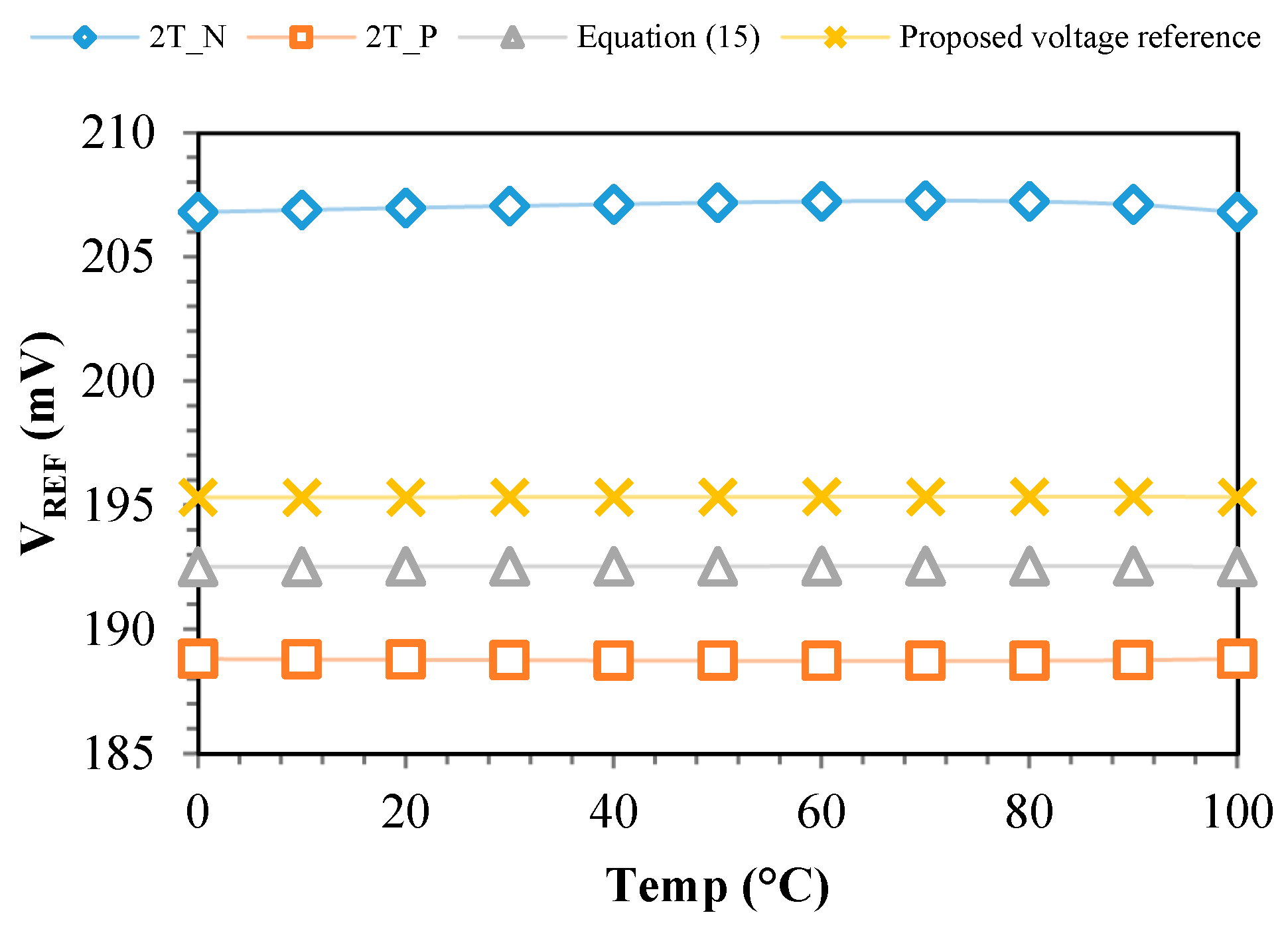
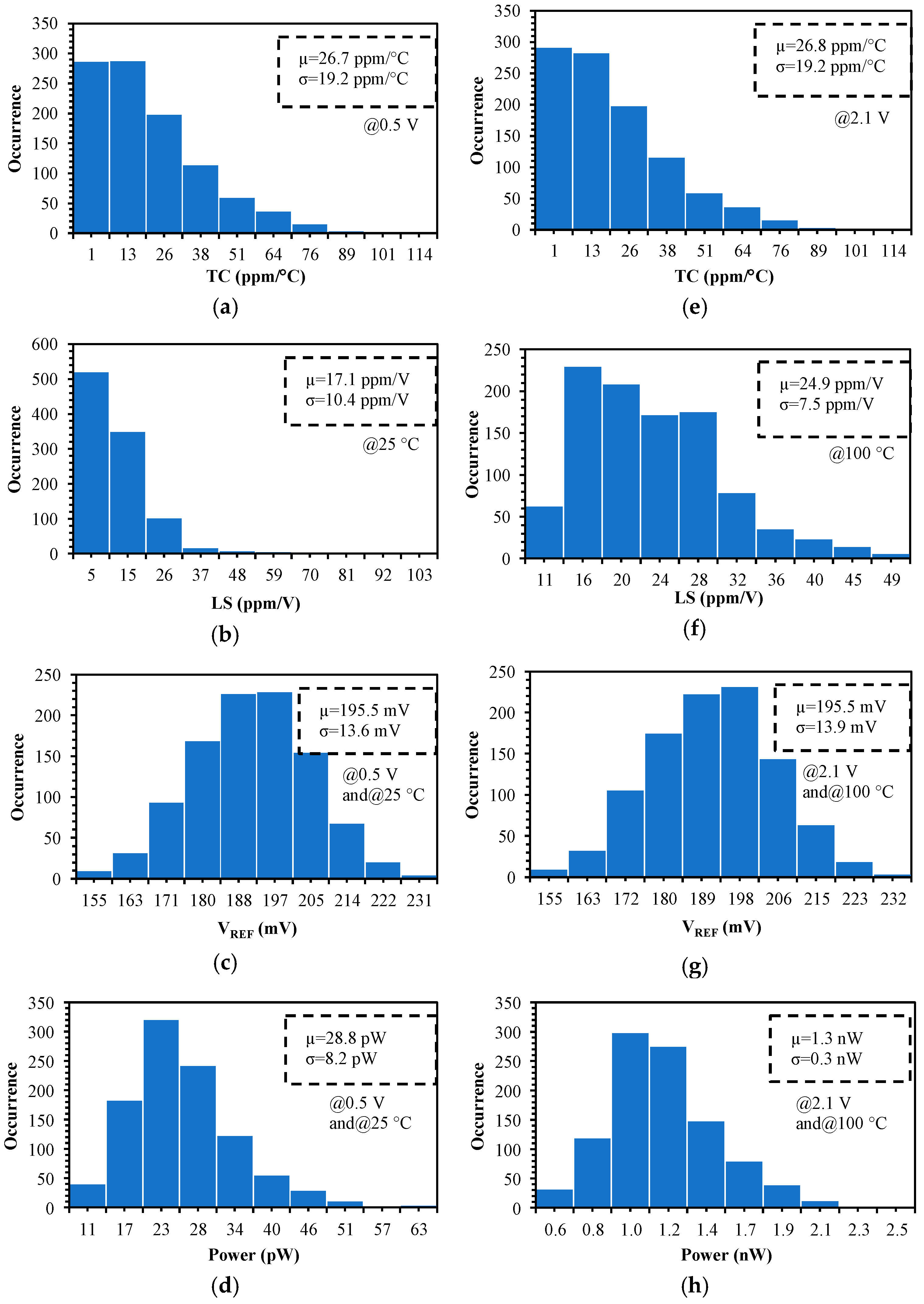
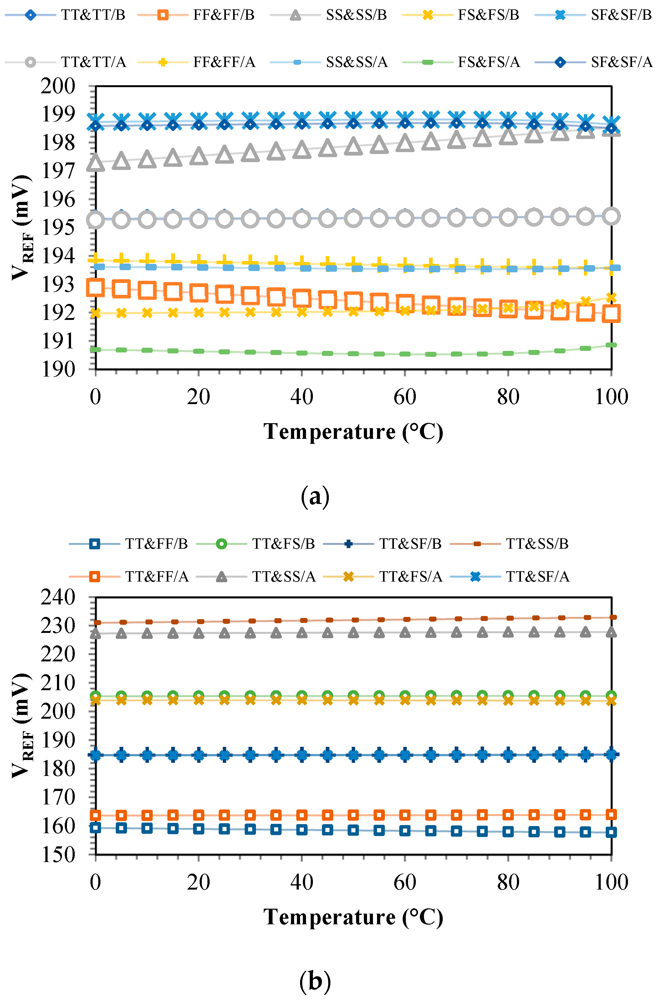
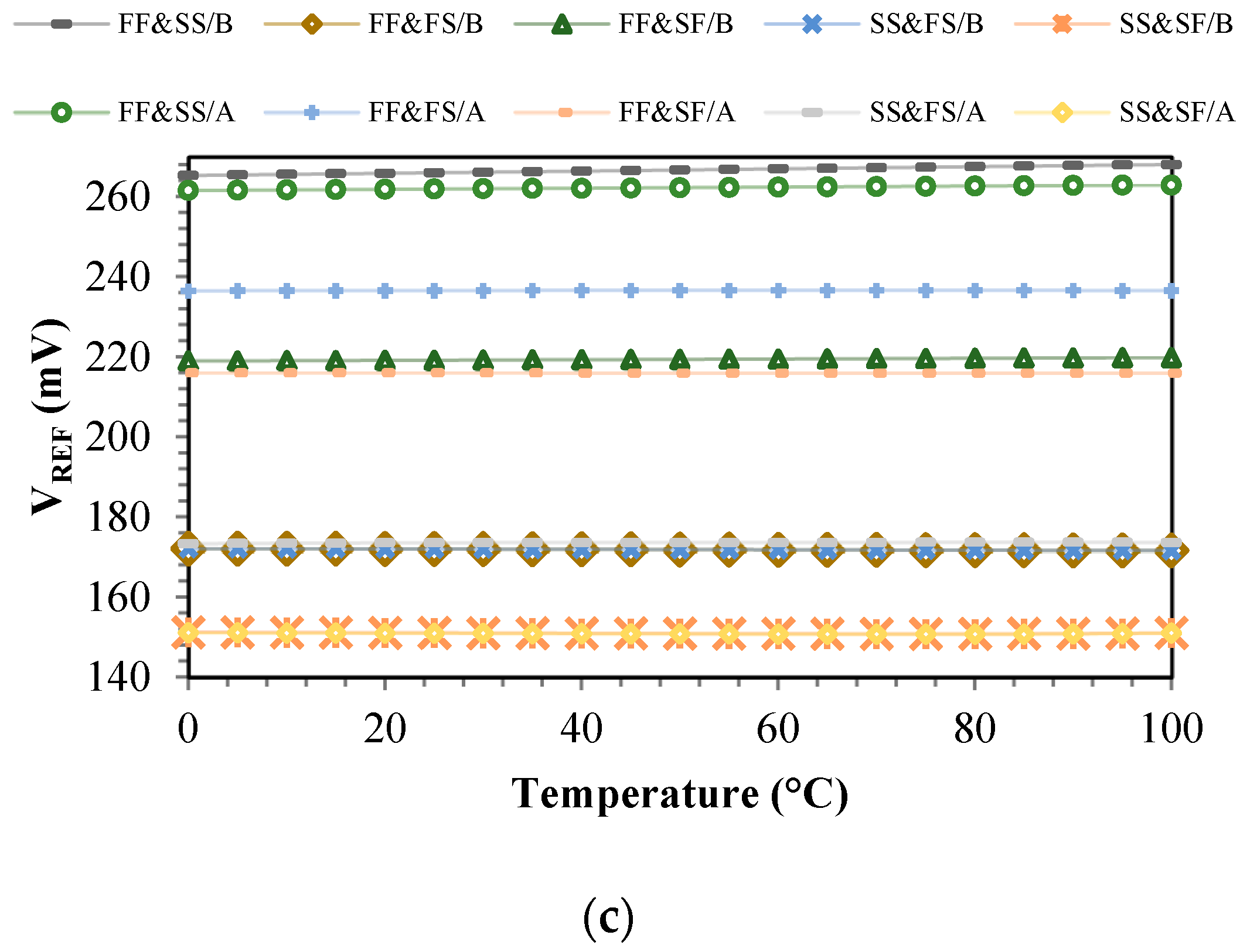
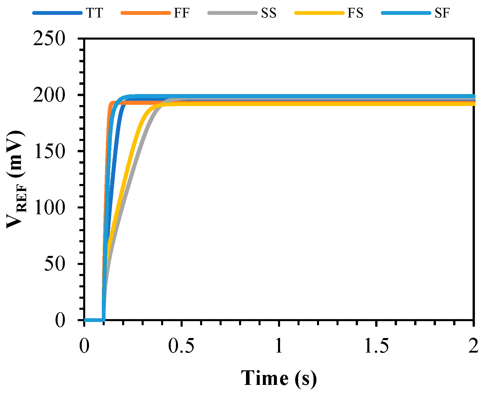
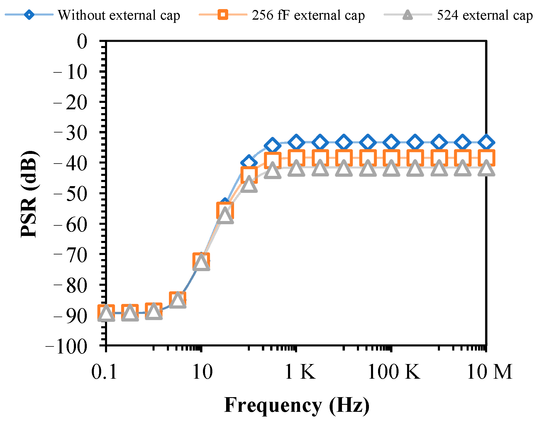
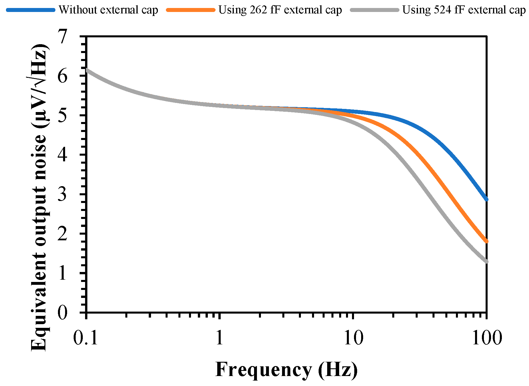
5. Simulation Results

The proposed two-stage voltage reference has been tested in 0.18 μm CMOS technology. Figure 11 depicts the proposed design layout, which occupies an area of 2358.8 µm2. This section presents the performance of the proposed reference obtained from post-layout simulations.
Figure 12 shows the variations in the output reference voltage against the temperature and supply voltage in the typical corner. The LS in the 0.5 V to 2.1 V supply voltage range at 25 °C is equal to 13.6 ppm/V, and the TC in the 0 °C to 100 °C temperature range at 0.5 V supply voltage is equal to 6.8 ppm/°C. In Figure 13, the TC changes with respect to the supply voltage are shown. The TC changes only 0.35 ppm/°C, with a variation in the supply voltage from 0.5 V to 2.1 V.
Monte Carlo analysis is used to investigate the effect of process and mismatch variations on TC, LS, power consumption, and the output reference voltage, as shown in Figure 14. In Figure 14a–d, the TC is reported in the temperature range from 0 °C to 100 °C at 0.5 V supply voltage, and the LS is simulated in the 0.5 V to 2.1 V supply voltage range at 25 °C. Power consumption and VREF are also shown at 0.5 V and 25 °C.
In Figure 14e–h, the maximum supply voltage and temperature scenarios are investigated. The results of the Monte Carlo analysis are summarized in Table 2. The bias current of the circuit branches and the resulting power consumption have been reduced to 28.8 pW at room temperature through the connection of the gate to the source of the transistors that act as current sources, namely transistors M5, M7, and M9. In addition to low power consumption, the proposed voltage reference has both low LS and TC of 17.1 ppm/V and 26.7 ppm/°C, respectively. As the supply voltage rises, the TC maintains a near-constant value, and there is a slight change in the LS as the temperature increases. When either the supply voltage or operating temperature increases, the power consumption will rise due to the temperature- and voltage-dependent bias current.
The use of a trimming network can significantly reduce the variations in the reference voltage by modifying the aspect ratio of M8. In [10], a suitable scenario for trimming the TC is proposed by removing the extra switches and eliminating variable parasitic diodes. When trimming transistors need to be in the off-state, using a sufficient negative voltage for source-gate transistors minimizes the effects on the output voltage behavior.
To examine the effect of a 3-bit TC trim circuit from [10] in reducing TC, a simple scenario is shown in Figure 15.
As the trim transistors apply a constant parasitic diode load to the output node independent of their state, this constant load can be compensated with the other parasitic diodes at the output. Given that the output voltage is approximately 0.2 V, the minimum source-gate voltage of the trim transistors while in the off-state is approximately −0.3 V. The currents I8, I8-0, I8-1, and I8-2 in the TT corner are illustrated in Figure 16 when M8-0 and M8-1 are in the off-state.
Notably, the currents flowing through the switched-off transistors are significantly lower than that of the voltage reference generator transistors. Consequently, the impact of these switched-off transistors on the output voltage can be neglected.
The TCs in the different corners are examined before and after the trim in Figure 17. Before trimming, the TC for TT&TT (first corners for thin oxide and second for thick oxide transistors), FF&FF, SS&SS, FS&FS, and SF&SF is 5.48 ppm/°C, 47.28 ppm/°C, 62.25 ppm/°C, 28.28 ppm/°C, and 8.82 ppm/°C, respectively. After trimming, they become 6.78 ppm/°C, 13.68 ppm/°C, 4.2 ppm/°C, 17.16 ppm/°C, and 9.43 ppm/°C, respectively. The average TC in these five corners before the trim is 30.42 ppm/°C, while after the trim, it becomes 10.25 ppm/°C. Furthermore, in other corners, such as FF&SF, as well as TT&SS, the trim circuit reduces the TC from 39.5 ppm/°C and 80.5 ppm/°C to 4.5 ppm/°C and 22.8 ppm/°C, respectively. Increasing the number of trim bits can further improve the TC of the circuit, but this comes at the cost of increasing the complexity and occupied area.
The startup times exhibiting the worst performance across various corners with 0.5 V supply voltage and at 0 °C are illustrated in Figure 18. The power supply is turned on at 100 ms. The startup time associated with SS has the highest value, at 341.4 ms.
Voltage references are used in analog and digital hybrid systems, so it is necessary to determine their sensitivity to fluctuations in the supply voltage. The M10 transistor is used as a 262 fF capacitor at the output node. At minimum supply voltage and room temperature (25 °C), the PSR from 0.1 Hz to 10 MHz is shown in Figure 19 without an external decoupling capacitor, double the output node capacitance (using an external 262 fF capacitor), and triple the output node capacitance (using an external 524fF capacitance). The PSR near-DC frequencies are very low due to the efficient LS compensation. The minimum PSR is −89.3 dB at 0.1 Hz in all cases, and at high frequencies, it increases due to the leakage capacitors of the transistors and, finally, without external decoupling, remains constant at about −33.3 dB capacitor and, by using the external 262 fF and 524 fF decoupling capacitor, it becomes −38.4 dB and −41.6 dB, respectively.
Figure 20 depicts the output noise within the frequency range of 0.1 Hz to 100 Hz, maintaining identical conditions to the PSR. The integrated noise from 0.1 Hz to 10 Hz without additional load capacitors, using the 262 fF external decoupling capacitor and 524 fF, respectively, generates 16.3 µV, 16.2 µV, and 16 µV. In the 0.1 Hz to 100 Hz range, it becomes 41.8 µV, 34.8 µV, and 30.3 µV, respectively. The output noise and PSR can decrease more if the load capacitor increases.
A comparison of the proposed voltage reference with all-MOSFET ultra-low-power designs is provided in Table 3. The proposed circuit has the best LS compared to the other voltage references. The LS of [20] is improved in the proposed voltage reference by a more accurate optimization to compensate for the DIBL effect. The proposed structure provides a TC of 26.7 ppm/°C without a TC trim circuit. After trimming, which needs more manufacturing and testing costs as well as more silicon area, [9,10,12] provide a more suitable TC. For [10] to operate correctly, a supply voltage of 0.8 V must be provided, and the power consumption associated with [9,12] exceeds that of the proposed design. The following FoM is used in Table 3 [10] to compare the voltage references with a number.
F o M = T m a x T m i n 2 T C × L S × P o w e r × 10 23   ° C · V W
It is evident from Table 3 that in trimless designs, the proposed technique shows the highest figure of merit (FoM), whereas when the trim is employed, the optimal FoM corresponds to that of reference [10]. The proposed structure improves both LS and TC while consuming just 28.8 pW.

6. Conclusions

This paper presents an all-MOSFET voltage reference in 0.18 µm CMOS. Combining 2T n-type and p-type voltage references alleviates the curvature changes in the output reference voltage versus temperature, and an optimized design has been adopted to compensate the DIBL effect in the first stage. The circuit performance is estimated by post-layout Monte Carlo simulations over 1000 runs. The average TC is 26.7 ppm/°C from 0 °C to 100 °C. On average, the LS is decreased to 17.1 ppm/V for supply voltages from 0.5 V to 2.1 V, confirming optimized DIBL effect compensation. Last but not least, the mean power consumption is 28.8 pW, which makes it suitable for ultra-low-power applications in energy-autonomous IoT sensor nodes, wearable devices, and medical implants.

Author Contributions

Writing—original draft, M.A.; Writing—review & editing, M.H. and P.C. All authors have read and agreed to the published version of the manuscript.

Funding

This research received no external funding.

Data Availability Statement

Data are contained within the article.

Conflicts of Interest

The authors declare no conflicts of interest.

References

  1. Palumbo, G. Voltage references: From diodes to precision high-order bandgap circuits [Book Review]. IEEE Circuits Devices Mag. 2002, 18, 45. [Google Scholar] [CrossRef]
  2. Akbari, M.; Hussein, S.M.; Hashim, Y.; Tang, K.-T. An enhanced input differential pair for low-voltage bulk-driven amplifiers. IEEE Trans. Very Large Scale Integr. (VLSI) Syst. 2021, 29, 1601–1611. [Google Scholar] [CrossRef]
  3. Mahmoudi, A.; Torkzadeh, P.; Dousti, M. A 6-bit 1.5-GS/s SAR ADC with smart speculative two-tap embedded DFE in 130-nm CMOS for wireline receiver applications. IEEE Trans. Very Large Scale Integr. (VLSI) Syst. 2021, 29, 871–882. [Google Scholar] [CrossRef]
  4. Chowdary, G.; Aashish, T.; Chatterjee, S. A 99% Current Efficient Three-Transistor Regulator With Built-In 80 ppm/° C Reference, for 0–10 mA Loads. IEEE Solid-State Circuits Lett. 2018, 1, 26–29. [Google Scholar] [CrossRef]
  5. De Oliveira, A.C.; Cordova, D.; Klimach, H.; Bampi, S. A 0.12–0.4 V, versatile 3-transistor CMOS voltage reference for ultra-low power systems. IEEE Trans. Circuits Syst. I Regul. Pap. 2018, 65, 3790–3799. [Google Scholar] [CrossRef]
  6. Olivera, F.; da Silva, L.S.; Petraglia, A. A 120 mV Supply, Triode-Regulated Femto-Watt CMOS Voltage Reference Design. IEEE Trans. Circuits Syst. II Express Briefs 2020, 68, 587–591. [Google Scholar] [CrossRef]
  7. Zhuang, H.; Liu, X.; Wang, H. Voltage reference with linear-temperature-dependent power consumption. IEEE Trans. Very Large Scale Integr. (VLSI) Syst. 2020, 28, 1043–1049. [Google Scholar] [CrossRef]
  8. Seok, M.; Kim, G.; Blaauw, D.; Sylvester, D. A portable 2-transistor picowatt temperature-compensated voltage reference operating at 0.5 V. IEEE J. Solid-State Circuits 2012, 47, 2534–2545. [Google Scholar] [CrossRef]
  9. de Oliveira, A.C.; Cordova, D.; Klimach, H.; Bampi, S. Picowatt, 0.45–0.6 V self-biased subthreshold CMOS voltage reference. IEEE Trans. Circuits Syst. I Regul. Pap. 2017, 64, 3036–3046. [Google Scholar] [CrossRef]
  10. Azimi, M.; Habibi, M.; Crovetti, P. pMOS-only pW-power voltage reference with sub-10 ppm/°C trimmed temperature coefficient and sub-100 ppm/V line sensitivity. Int. J. Circuit Theory Appl. 2023, 51, 2638–2653. [Google Scholar] [CrossRef]
  11. Dastgerdi, M.A.; Habibi, M.; Dolatshahi, M. A novel two stage cross coupled architecture for low voltage low power voltage reference generator. Analog Integr. Circuits Signal Process. 2019, 99, 393–402. [Google Scholar] [CrossRef]
  12. Wang, Y.; Sun, Q.; Luo, H.; Wang, X.; Zhang, R.; Zhang, H. A 48 pW, 0.34 V, 0.019%/V line sensitivity self-biased subthreshold voltage reference with DIBL effect compensation. IEEE Trans. Circuits Syst. I Regul. Pap. 2019, 67, 611–621. [Google Scholar] [CrossRef]
  13. Ji, Y.; Lee, J.; Kim, B.; Park, H.-J.; Sim, J.-Y. A 192-pW Voltage Reference Generating Bandgap–Vth With Process and Temperature Dependence Compensation. IEEE J. Solid-State Circuits 2019, 54, 3281–3291. [Google Scholar] [CrossRef]
  14. Dong, Q.; Yang, K.; Blaauw, D.; Sylvester, D. A 114-pW PMOS-only, trim-free voltage reference with 0.26% within-wafer inaccuracy for nW systems. In Proceedings of the 2016 IEEE Symposium on VLSI Circuits (VLSI-Circuits), Honolulu, HI, USA, 15–17 June 2016; pp. 1–2. [Google Scholar]
  15. Bhattacharjee, I.; Chowdary, G. A 0.3 nW, 0.093%/V Line Sensitivity, Temperature Compensated Bulk-Programmable Voltage Reference for Wireless Sensor Nodes. IEEE Trans. Very Large Scale Integr. (VLSI) Syst. 2022, 30, 1281–1293. [Google Scholar] [CrossRef]
  16. Qiao, H.; Zhan, C.; Chen, Y. A− 40 °C to 140 °C Picowatt CMOS Voltage Reference With 0.25-V Power Supply. IEEE Trans. Circuits Syst. II Express Briefs 2021, 68, 3118–3122. [Google Scholar] [CrossRef]
  17. Chen, H.-M.; Lee, C.-C.; Jheng, S.-H.; Chen, W.-C.; Lee, B.-Y. A sub-1 ppm/° C precision bandgap reference with adjusted-temperature-curvature compensation. IEEE Trans. Circuits Syst. I Regul. Pap. 2017, 64, 1308–1317. [Google Scholar] [CrossRef]
  18. Magnelli, L.; Crupi, F.; Corsonello, P.; Iannaccone, G. A sub-1 V nanopower temperature-compensated sub-threshold CMOS voltage reference with 0.065%/V line sensitivity. Int. J. Circuit Theory Appl. 2015, 43, 421–426. [Google Scholar] [CrossRef]
  19. Magnelli, L.; Crupi, F.; Corsonello, P.; Pace, C.; Iannaccone, G. A 2.6 nW, 0.45 V temperature-compensated subthreshold CMOS voltage reference. IEEE J. Solid-State Circuits 2010, 46, 465–474. [Google Scholar] [CrossRef]
  20. Azimi, M.; Habibi, M.; Karimi-Alavijeh, H.R. A 0.4 V, 19 pW subthreshold voltage reference generator using separate line sensitivity and temperature coefficient correction stages. AEU-Int. J. Electron. Commun. 2021, 140, 153949. [Google Scholar] [CrossRef]
  21. Razavi, B. Design of Analog CMOS Integrated Circuits, 2nd ed. McGraw-Hill: New York, NY, USA, 2017.
  22. Aminzadeh, H. Subthreshold reference circuit with curvature compensation based on the channel length modulation of MOS devices. Int. J. Circuit Theory Appl. 2022, 50, 1082–1100. [Google Scholar] [CrossRef]
  23. Tsividis, Y. Operation and Modeling of the MOS Transistor; Oxford University Press: Oxford, UK, 1999. [Google Scholar]
  24. Haartman, M.V.; Östling, M.; Haartman, M.v.; Östling, M. 1/F Noise in Mosfets: Origins and modeling. In Low-Frequency Noise In Advanced Mos Devices; 2007; Springer: Berlin/Heidelberg, Germany; pp. 53–102. [Google Scholar]
  25. Fassio, L.; Lin, L.; De Rose, R.; Lanuzza, M.; Crupi, F.; Alioto, M. Trimming-less voltage reference for highly uncertain harvesting down to 0.25 V, 5.4 pW. IEEE J. Solid-State Circuits 2021, 56, 3134–3144. [Google Scholar] [CrossRef]
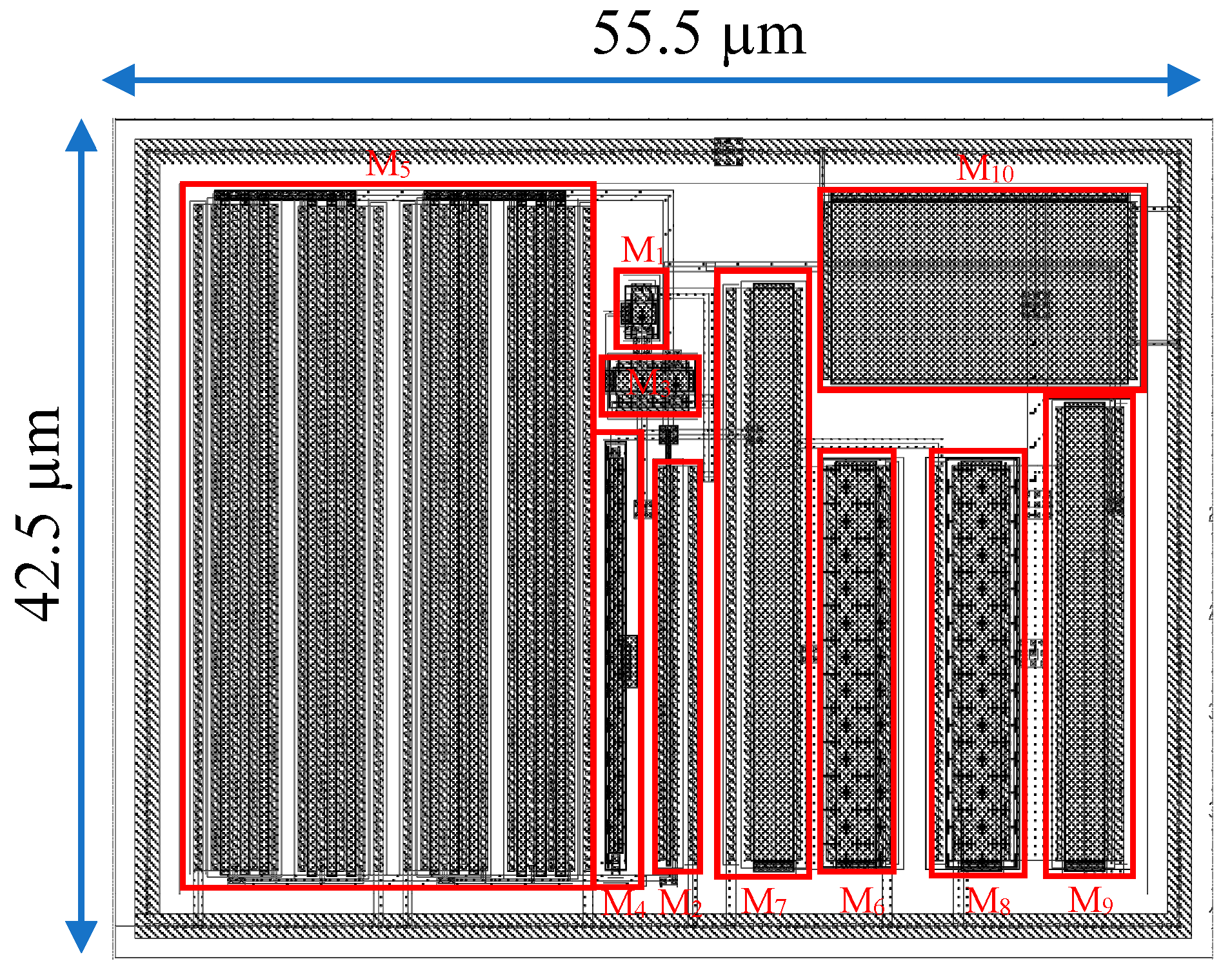
Figure 1. A two-stage circuit with DIBL effect compensation was proposed in [20].
Electronics 13 01390 g001
Figure 2. Simulation results of VREG and VX versus supply voltage.
Electronics 13 01390 g002
Figure 3. Adjusting L5 and W3 to satisfy Equations (8) and (9) using Monte Carlo analysis at each point on the graph.
Electronics 13 01390 g003
Figure 4. Simulation results of (a) 2T n-type reference output voltage versus temperature for different widths of M7; (b) 2T p-type reference output voltage versus temperature for different widths of M9.
Electronics 13 01390 g004
Figure 5. Linearization of 2 Φ F + V B S for VBS from 0 to 200 mV.
Electronics 13 01390 g005
Figure 6. Simulation of the threshold voltage of M8 with respect to VBS8.
Electronics 13 01390 g006
Figure 7. ΔVTH8 between two bias modes: with body bias through output voltage of a 2T n-type reference and with zero body bias.
Electronics 13 01390 g007
Figure 8. The complete architecture of the proposed voltage reference circuit.
Electronics 13 01390 g008
Figure 9. The compensated output reference voltage of 2T n-type and p-type, the predicted value through the sum of the output voltages of 2T n-type and p-type according to Equation (15), and the output reference voltage.
Electronics 13 01390 g009
Figure 10. TC Monte Carlo analysis with 100 runs for two parameters of W7 and W9 and temperature compensation prediction of (22).
Electronics 13 01390 g010
Figure 11. Proposed voltage reference layout.
Electronics 13 01390 g011
Figure 12. Variations in reference voltage against supply voltage from 0.3 V to 2.1 V and against temperature from 0 °C to 100 °C.
Electronics 13 01390 g012
Figure 13. TC changes versus supply voltage.
Electronics 13 01390 g013
Figure 14. Monte Carlo analysis with 1000 runs on process and mismatch of post-layout.
Electronics 13 01390 g014
Figure 15. TC correction stage using a 3-bit trimming TC circuit.
Electronics 13 01390 g015
Figure 16. Comparison of the current of the trim transistors in the off-state with the on-state and the current of the M8 transistor when the supply voltage is 0.5 V.
Electronics 13 01390 g016
Figure 17. Variations in reference output voltage versus temperature in different corners before and after trim. The figure legend lists the transistor corners with thin oxide first, followed by those with thick oxide, using keywords A for after trim and B for before trim. (a) Main corners, (b) TT for thin oxide with some other corners for thick oxides, and (c) FF and SS for thin oxide with some other corners for thick oxides.
Electronics 13 01390 g017aElectronics 13 01390 g017b
Figure 18. The startup time of the reference voltage at 0 °C and different corners when the minimum supply voltage (VDD = 0.5 V) is turned on at 0.1 s.
Electronics 13 01390 g018
Figure 19. PSR of the proposed design at 0.5 V supply voltage, 25 °C, and for frequencies from 0.1 Hz to 10 MHz.
Electronics 13 01390 g019
Figure 20. Output noise from 0.1 Hz to 100 Hz.
Electronics 13 01390 g020
Table 1. Summary of post-layout Monte Carlo analysis (1000 runs).
TransistorType Size
M1Thick oxide1 µm/1 µm
M2Thin oxide20 µm/0.18 µm
M3Thick oxide3.7 µm/1 µm
M4Thick oxide0.22 µm/20 µm
M5Thin oxide(101.1 µm/0.45 µm) × 4
M6Thick oxide20 µm/2 µm
M7Thin oxide29 µm/2 µm
M8Thick oxide20 µm/2 µm
M9Thin oxide23 µm/2 µm
M10Thin oxide9 µm/15 µm
Table 2. Summary of post-layout Monte Carlo analysis (1000 runs).
Parametersµσσ/µ
TC (ppm/°C) @0.5 V26.719.271.9%
@2.1 V26.819.271.6%
LS (ppm/V) @25 °C17.110.460.8%
@100 °C24.97.530.1%
VREF (mV) @0.5 V and 25 °C195.513.67%
@2.1 V and 100 °C195.513.97.1%
Power (pW) @0.5 V and 25 °C28.88.228.5%
@2.1 V and 100 °C130830523.3%
Table 3. Comparison of the proposed voltage reference with similar ones.
DesignThis Work *[6] *[12][20] *[16][8][25][9][10] *
Tech (µm)0.180.180.180.180.180.130.180.180.18
Min supply (V)0.50.120.60.40.250.50.250.60.8
LS (ppm/V)
µ17.12200 190143.830003301600110051.7
360 T 51.5 T
σ10.4-6017.3--500-10.8
10 T
Power (pW)28.80.254819.11132.2
29.5 T
5.466425.9
25.9 T
Temp range (°C)0–100−40–1200–1000–80−40–140−20–800–1200–120−20–80
TC (ppm/°C)
µ26.789.815239.273.56226549534.3
10.1 T- 29 T 11.6 T4.4 T
σ19.211.7192811.74145-26.5
1.5 T- 11 1.4 T7 T
PSR (dB)
@10 Hz−72 C−78 C−62.7 C−90.9-−50.5 C−70−45 C−41.2
@10 KHz−33.3 C−96 C−50.2 C−78-−58.5 C−83.5−55 C−25.6
VREF (mV)195.565.7147.9 T119.2118.117691.4457.1 T206 T
Area (µm2)2358.87033,200218392493002200170010,208
FoM (°C·V/W)
Before trim7.615.180.220.590.012.220.060.0012.18
After trim--1.08--0.32-0.0216.97
TT corner; T After trim; C using decoupling capacitor; * Monte Carlo simulation.
Disclaimer/Publisher’s Note: The statements, opinions and data contained in all publications are solely those of the individual author(s) and contributor(s) and not of MDPI and/or the editor(s). MDPI and/or the editor(s) disclaim responsibility for any injury to people or property resulting from any ideas, methods, instructions or products referred to in the content.

