Abstract
We conducted a comparative study on the characterization of Ga-polar and N-polar GaN metal–insulator–semiconductor (MIS) Schottky contact with a SiNx gate dielectric. The correlation between the surface morphology and the current–voltage (I–V) characteristics of the Ga- and N-polar GaN Schottky contact with and without SiNx was established. The insertion of SiNx helps in reducing the reverse leakage current for both structures, even though the leakage is still higher for N-polar GaN, consistent with the Schottky barrier height calculated using X-ray photoelectron spectroscopy. To optimize the electric property of the N-polar device, various substrate misorientation angles were adopted. Among the different misorientation angles of the sapphire substrate, the GaN MIS Schottky barrier diode grown on 1° sapphire shows the lowest reverse leakage current, the smoothest surface morphology, and the best crystalline quality compared to N-polar GaN grown on 0.2° and 2° sapphire substrates. Furthermore, the mechanism of the reverse leakage current of the MIS-type N-polar GaN Schottky contact was investigated by temperature-dependent I–V characterization. FP emissions are thought to be the dominant reverse conduction mechanism for the N-polar GaN MIS diode. This work provides a promising approach towards the optimization of N-polar electronic devices with low levels of leakage and a favorable ideality factor.
1. Introduction
Gallium nitride (GaN) has attracted a tremendous amount of attention in the past decade in applications including power switching and RF devices due to its wide bandgap, high electron saturation velocity, and large electric field breakdown [1,2]. Among various factors, high-quality Schottky contact is one of the most critical aspects in the evaluation of device performance [3,4,5]. However, due to the existence of very dense trap states at the metal–semiconductor (MS) interface, Schottky barrier height is significantly reduced due to the trap-assisted tunneling effect and Fermi level pinning, preventing us from understanding the interface’s properties and jeopardizing device performance [6]. To tackle above-mentioned issue, a variety of gate dielectrics, such as Al2O3 [7], SiNx [8], ZrO2 [9], and HfO2 [10], have been proposed, acting as an insulator layer at the MS interface. But most of them are fabricated on Ga-polar GaN thin films.
Due to the non-centrosymmetric crystal structure of wurtzite III-nitride, distinguishable gallium and nitrogen polarities with opposite, spontaneous, and piezoelectric polarizations have been revealed along the c-axis of GaN thin films [11,12]. In the pursuit of high-performance GaN electronic devices over the past decade, Ga-polar thin films have been widely utilized as a mature growth technology with a smoother surface morphology and better crystalline quality. Researchers have shown tremendous interest in the growth of N-polar devices due to their unique characteristics, including their low contact resistivity [13,14,15], opposite spontaneous polarization, and naturally forming back barrier in power electronic devices [16]. However, N-polar GaN Schottky contacts are strongly influenced by surface polarization charges and surface morphology [17,18]. Reddy et al. demonstrated that the Schottky barrier height of III-polar GaN is higher than that of a non-polar surface and even higher than that of a N-polar thin film via the accurate modeling of the valence band edge and a comparison with XPS data [19]. Khachariya et al. investigated the effect of different chemical treatments on the Schottky contact behaviors of N-polar GaN, revealing that the barrier height increases as the surface roughness increases [18]. The above results clearly indicate the importance of the modulation of surface morphology and surface states toward N-polar GaN devices with better properties [20,21]. The usage of dielectric layers in the N-polar Schottky contact, i.e., the formation of an MIS-type structure, seems to be a promising option, but there unfortunately is a lack of in-depth understanding on their electric behaviors. Furthermore, since the surface diffusion length in N-polar GaN is much smaller than that of Ga-polar GaN, N-polar GaN is prone to exhibit the 3D island growth mode, leading to much a higher surface roughness value, which is unsuitable for uniform dielectric layer deposition. This, however, can be tackled by either changing the substrate with a smaller terrace width to facilitate the step-flow growth mode, using an AlN nucleation layer with different thicknesses [22], or modulating the growth condition such as the V/III ratio [23,24], thus promoting the surface migration of the adsorbed atoms. Keller et al. reported that a smooth surface can be obtained through the utilization of vicinal sapphire substrates misoriented toward the a or m directions [25]. Despite the successful growth of smooth N-polar GaN, reports on N-polar power electronics or even dielectric/N-polar GaN heterostructures are scarce. Mohanty et al. fabricated a 20 nm HfO2/GaN metal–insulator–semiconductor capacitor through the ALD technique, demonstrating that pre-deposition cleaning, such as wet etching, plasma treatment, or surface annealing, is critically important for an ideal dielectric/N-polar GaN interface with a greatly reduced interface trap density [26]. Yet ALD is an inherently conformal thin film deposition technique. When industry-friendly LPCVD or PECVD were used for dielectric deposition, the thin film quality was extremely sensitive to the surface condition of N-polar GaN, which has been less investigated so far. Overall, the techniques to improve the performance of a N-polar MIS Schottky diode remain elusive due to the relatively poor crystalline quality and rough surface morphology of N-polar thin films, hampering a precise evaluation of influencing factors. Furthermore, little is known regarding the underlying mechanism that is responsible for the different electrical behaviors of Ga-polar and N-polar Schottky contacts.
In this work, a comparative study on the electrical behaviors between Ga-polar and N-polar GaN/SiNx/NiAu MIS-type Schottky contacts were performed. Energy band diagrams and corresponding barrier heights were evaluated based upon an XPS analysis and current–voltage characterization. The influences of the substrate offcut angle on the surface morphology, crystalline quality, and electrical behaviors of N-polar MIS-Schottky diodes were revealed. The reverse-bias tunneling mechanism was further demonstrated by their temperature-dependent I–V characteristics, and our experimental results were corroborated through computer-aided design simulations, providing guidance for the design and optimization of N-polar electronic devices.
2. Materials and Methods
Unintentionally doped GaN was grown on 2-inch sapphire substrate in a low-pressure metalorganic chemical vapor deposition (MOCVD) reactor. Trimethylgallium and ammonia are used as the Ga and N sources, respectively. A mixture of nitrogen and hydrogen is used as the carrier gas. Prior to Ga-polar GaN deposition, a low-temperature AlN nucleation layer (NL) was coated on sapphire substrate via reactive sputtering, while N-polar GaN was obtained by direct epitaxy on bare sapphire substrate with proper thermal annealing and nitridation. The detailed polarity control technique can be found in previous literature [27,28]. Prior to SiNx dielectric deposition, the GaN surfaces were treated using acetone, methanal, and DI water to remove organic residuals and particles. GaN thin films were then dipped into diluted hydrochloric acid (HCl) to remove the naturally formed oxide. SiNx dielectrics that were 6 nm thick were deposited on GaN surface by either low-pressure chemical vapor deposition (LPCVD) or plasma-enhanced chemical vapor deposition (PECVD). Ohmic contact comprising Ti/Al/Ni/Au stacks was deposited on the exposed GaN surface by e-beam evaporation technique, and Schottky Ni/Au stacks were evaporated on the dielectric layer.
Top-view and cross-sectional schematics of the MIS-type Schottky contact are illustrated in Figure 1a and b, respectively. The diameter of the Schottky contact is 500 µm and the distance between circular Schottky contact and ring-shaped ohmic contact is 20 µm. The fabrication process is shown in Figure 1c. For the purpose of comparison, two reference MS-type Schottky contacts without the insertion of SiNx were also fabricated based on Ga-polar and N-polar GaN. To survey the quality of Ga- and N-polar GaN, a Veeco Dimension 3100V atomic force microscope (Bruker Inc., Billerica, MA, USA) and a Bruker D8 Discover high-resolution X-ray diffractometer (HRXRD) (Bruker Inc., Billerica, MA, USA) were utilized. The current–voltage (I–V) measurements were performed using a Keithley 4200 SourceMeter equipped with a probe station (Tektronix Inc., Beaverton, OR, USA). The lateral band diagram is calculated by the data collected from Kratos AXIS X-ray photoelectron spectroscopy (XPS) system with an Al Kα radiation source (Shimadzu Corporation, Tokyo, Japan).
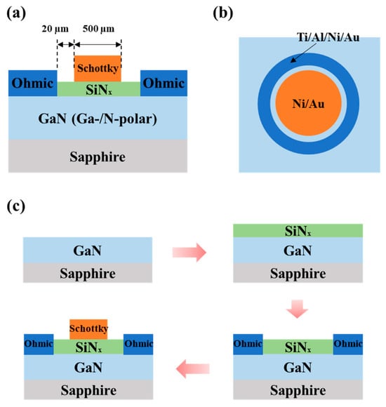
Figure 1.
(a) Cross-sectional and (b) top-view schematics of the MIS-type Schottky contact; (c) Schematic of process flow when fabricating the heterostructure.
3. Results and Discussion
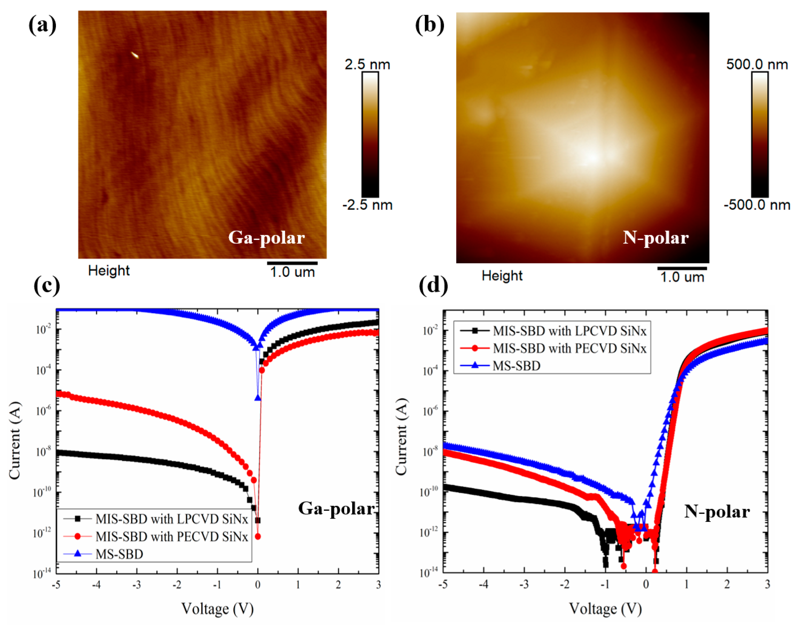
The AFM images of the Ga- and N-polar surfaces of the GaN thin films are shown in Figure 2a and b, respectively. It is shown that the Ga-polar surface has bi-layer steps with a roughness less than 0.15 nm, while the N-polar GaN surface is covered with hexagon hillocks that are several micrometers wide and have a roughness of 3.3 nm. Optical microscopy images revealing the distribution and density of the hillocks are shown in the supporting information section within Figure S1. The density of a hillock is approximately 5.02 × 10³/cm2. The drastic differences between GaN surface morphologies with opposite polarities are ascribed to the different surface diffusion lengths of Ga atoms [29]. Herein, a step-flow growth mode is obtained in the Ga-polar GaN, while the 3D column growth mode is usually observed in the N-polar surface. Furthermore, due to the inherently easier incorporation of oxygen impurities in the N-polar surface in comparison with its Ga-polar counterpart, the N-polar GaN exhibits a higher background carrier concentration, which is consistent with that of the previous literature [20]. In this work, the electron concentrations in the N- and Ga-polar GaN are identified as 2 × 1019 cm−3 and 3 × 1018 cm−3 via the Hall system. As a result, the N-polar thin film is expected to have better ohmic contact.
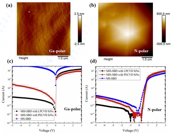
Figure 2.
(a,b) Surface morphologies of Ga-polar and N-polar GaN in 20 × 20 µm2 region; (c,d) I–V characteristics of the MIS-type Schottky diodes on Ga-polar and N-polar GaN.
In regards to gate dielectric deposition, the PECVD and LPCVD techniques have both been utilized in GaN electronic devices. Due to the relatively higher temperature and absence of plasma during thin film deposition, higher-quality SiNx is usually expected when using the LPCVD technique [30,31]. On the other hand, PECVD has the benefits of a high deposition rate and is compatible with the BEOL process [32]. In this work, both PECVD and LPCVD were adopted for SiNx deposition, and the I–V characteristics were compared. The log-scale current–voltage (I–V) characteristics of the MIS-type Schottky diodes on Ga- and N-polar GaN without and with a SiNx dielectric layer are summarized in Figure 2c,d. For the MS-type Schottky contact, a rectifying characteristic is observed in the Ga-polar GaN, while the reverse current is on the same level as the forward current for the N-polar GaN, indicating a much lower Schottky barrier at the Ni/N-polar GaN interface. The insertion of the SiNx dielectric significantly decreases the reverse-bias current for both samples. In comparison with the SiNx deposited using PECVD, the utilization of LPCVD provides a much lower reverse leakage current. The reverse leakage current at −5 V for the Ga-polar Schottky diode with SiNx using LPCVD reaches 1.3 × 10⁻⁷ A/cm2, and the specific forward on-state resistance (Ron) is 9032 mΩ·cm2. For the N-polar Schottky diode, the reverse leakage current is 5.1 × 10⁻⁶ A/cm2, and the Ron is 314 mΩ·cm2. Note that the on-state resistances of our samples are higher than those reported in other works in the literature [14,33,34], possibly originating from the absence of a thermal annealing process for the ohmic contacts. Nevertheless, the purpose of this work is to provide a comparative study on the electrical behaviors between Ga- and N-polar Schottky contacts. Thus, the absolute value of the Ron is less meaningful. As a result, the N-polar device exhibits a larger leakage current but a smaller Ron, possibly due to the smaller barrier height induced by the opposite polarization direction. Two major conclusions can be clearly demonstrated from the above results: first, a high-quality SiNx as the dielectric layer is critically important, which will suppress the leakage current to a great extent; and secondly, the N-polar thin film has a good forward electrical behavior at the expense of a larger leakage current, which further necessitates the utilization of a gate dielectric during device fabrication.
To distinguish the underlying mechanism for the drastically different electrical behaviors of Ga- and N-polar MIS Schottky contacts, energy band diagrams at the Ni/SiNx/GaN heterojunction interface are required, along with the band offset between SiNx and GaN ( and ) as well as the critical values. The band offset calculated by the XPS technique requires measurements of core level and valence band (VB) maximum binding energies on the surface of thick SiNx and GaN and at the interface formed by deposition of very thin SiNx on GaN. The valence band offset is determined by Equation (1), and the corresponding conduction band offset can be calculated with the information on the bandgaps, as shown in Equation (2) [35]:
and are the bandgaps of SiNx and GaN, respectively, and the subscripts and represent the core level and valence band maximum energies, respectively. Superscripts and indicate the interface and bulk film properties. Si 2p and Ga 2p were utilized during the calculation of the SiNx and GaN core levels using XPS. Since the penetration depth of XPS is only several nanometers, the thin SiNx can hardly form a uniform coating on top of the GaN. Therefore, a gradual ion etching of the 6 nm SiNx on GaN is performed before the core level of the Ga 2p peak emerges at the SiNx/GaN interface. BB is defined as the upward (positive) or downward (negative) bending of conduction band relative to the Fermi level at the SiNx/GaN interface. The equation is noted as follows:
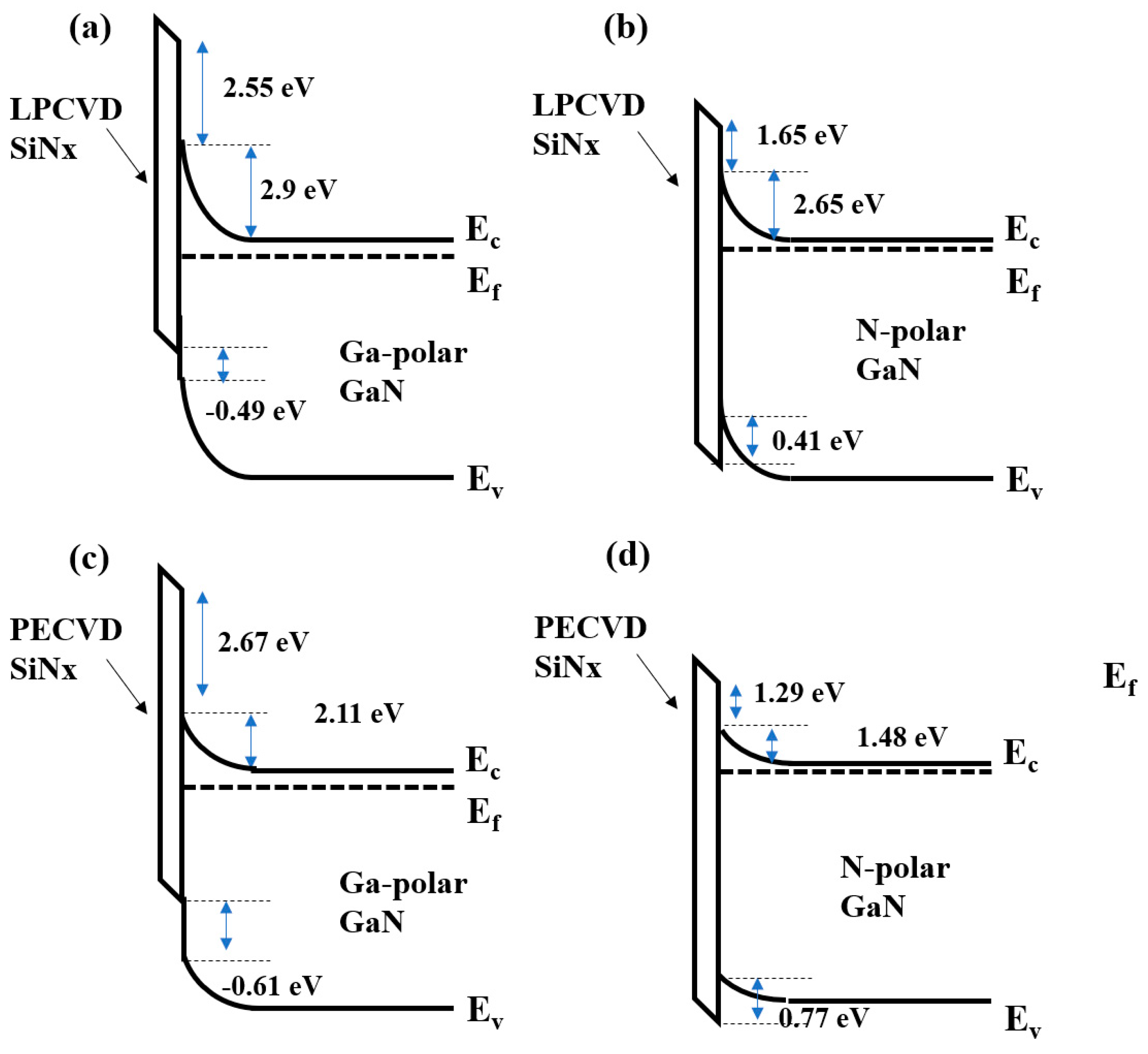
represents the relative position of the conduction band (Ec) to the Fermi level (Ef) in the bulk material and is directly related to the background carrier concentration. Table 1 summarizes the core levels and valence band maximum energies of both SiNx and GaN. The bandgap of SiNx is characterized using the Tauc technique in which a 10 nm thin SiNx layer was deposited on double-side polished sapphire substrate. The bandgap is calculated to be 5.5 eV. Based on these parameters, the energy band diagram can finally be drawn as shown in Figure 3. Taking LPCVD SiNx as an example, the band diagrams of the SiNx/Ga-polar GaN and SiNx/N-polar GaN interface are shown in Figure 3a and Figure 3b, respectively. The band alignment of SiNx on the Ga-polar GaN is a Type II staggered configuration, in which case a large of 2.55 eV was calculated, thereby providing a strong electron barrier. On the other hand, the Type I band offset is obtained for SiNx on the N-polar GaN, with a smaller of 1.65 eV. The band bends upwards in both cases, meaning there is a depletion of electrons at the interface. Combining the values of and BB, a much larger barrier height for the Ga-polar GaN than the N-polar GaN is achieved when the MIS-type Schottky diode is reverse biased. This agrees well with the I–V characteristic shown in Figure 2, in which the reverse leakage current is significantly higher in the N-polar configuration. The band diagrams of the PECVD SiNx/Ga-polar GaN and SiNx/N-polar GaN are also shown in Figure 3c and Figure 3d, respectively. The band alignments are similar to those of the LPCVD SiNx, but the band bending is weaker. For Ga-polar GaN, the BB decreases from 2.9 to 2.11 eV when the LPCVD method was replaced by the PECVD method; for the N-polar GaN, the value decreases from 2.65 to 1.48 eV. The higher band bending in the LPCVD SiNx is consistent with its lower reverse-based leakage current, suggesting that LPCVD is a more desirable technique for MIS-type structure fabrication.

Table 1.
Summary of core level and valence band maximum energies of GaN and SiNx (unit: eV).
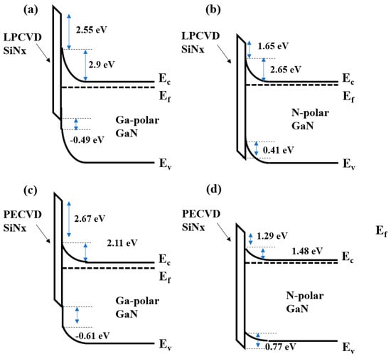
Figure 3.
Calculated band diagrams of (a) LPCVD SiNx deposited on Ga-polar GaN MIS-type Schottky contact, (b) LPCVD SiNx deposited on N-polar GaN MIS-type Schottky contact, (c) PECVD SiNx deposited on Ga-polar GaN MIS-type Schottky contact, and (d) PECVD SiNx deposited on N-polar GaN MIS-type Schottky contact.
As demonstrated above, due to the much smaller conduction band offset, the electron blocking effect in the N-polar MIS Schottky contact is weaker compared to that of its Ga-polar counterpart. This is mainly attributed to the inherently different surface states within the different band bending behaviors in the Ga- and N-polar surfaces. Upward band bending is identified on both the Ga-polar and N-polar GaN [36,37]. However, the large amount of surface states on the N-polar GaN compensates for the polarization-induced surface charges, leading to a weaker band bending effect. The trend is the same even with the insertion of SiNx. Secondly, as identified from Figure 3, the Schottky barrier of the LPCVD SiNx/GaN structure is higher than that of the PECVD SiNx/GaN structure. The possible reasons for this are as follows: The deposition temperature of the LPCVD SiNx is above 700 °C, in which case almost all of the NH3 in the chamber decomposes; thus, very few hydrogen atoms enter into the SiNx [38]. For PECVD, the deposition temperature is below 400 °C. The low deposition temperature results in a high rate of H incorporation in the SiNx. It has been reported that the N-H bonds formed in the SiNx layer can generate positive charges [39], thereby weakening the Schottky barrier height when in contact with GaN. Furthermore, nitrogen vacancies are also more frequently identified in PECVD SiNx due to the existence of plasma during thin film deposition as well as the low temperature [40]. These vacancies are manifested as shallow donor states in GaN, which also introduce positive charges and decrease the Schottky barrier height.
As mentioned in Figure 2, the N-polar GaN exhibits the 3D column growth mode due to having a smaller surface diffusion length. This can be mitigated by the modification of misorientation angles [41]. By enhancing the substrate misorientation angle, the width of the terraces is reduced. When the widths become smaller compared to the surface diffusion length of the adsorbed atoms, a bi-layer step or even the step bunching growth mode are expected [42]. Therefore, MIS-type Schottky barrier diodes based on different substrate misorientation angles, including 0.2°, 1°, and 2°, are prepared. These three offcut angles are more commercially available compared to other offcut angles; therefore, these were used for our study. With an offcut angle above 2°, N-polar GaN reveals a degraded crystal quality and surface morphology according to previous studies in the literature [11,25,43]. It is shown in Figures S2 and S3 in the supporting information that the surface roughness of the N-polar GaN grown on the 1° offcut sapphire is the lowest, and its crystal quality is also the highest. This result indicates the optimum substrate condition during the preparation of MIS-type SBD diodes. Surface morphologies of these samples are shown in Figure S1 in the supporting information section. When the N-polar GaN is grown on the 1° misoriented sapphire, a much smoother surface morphology is revealed. Further increasing the misoriented angle to 2° leads to step-bunching features due to greatly reduced surface supersaturation during its growth. It is noted that a smoother surface morphology not only benefits the uniform deposition of the SiNx dielectric layer, eliminating the possible occurrence of Schottky barrier inhomogeneity as previously reported [3,44] but also leads to a better crystal quality and herein a lower density of interface states. As shown in Figure S2, the full width at half maximum values of the (002) rocking curves for the N-polar GaN grown on 0.2°, 1°, and 2° misoriented sapphires are 511, 299, and 389, arcsec respectively, suggesting that the N-polar GaN grown on the 1° misoriented substrates serves as an ideal platform for device fabrication.
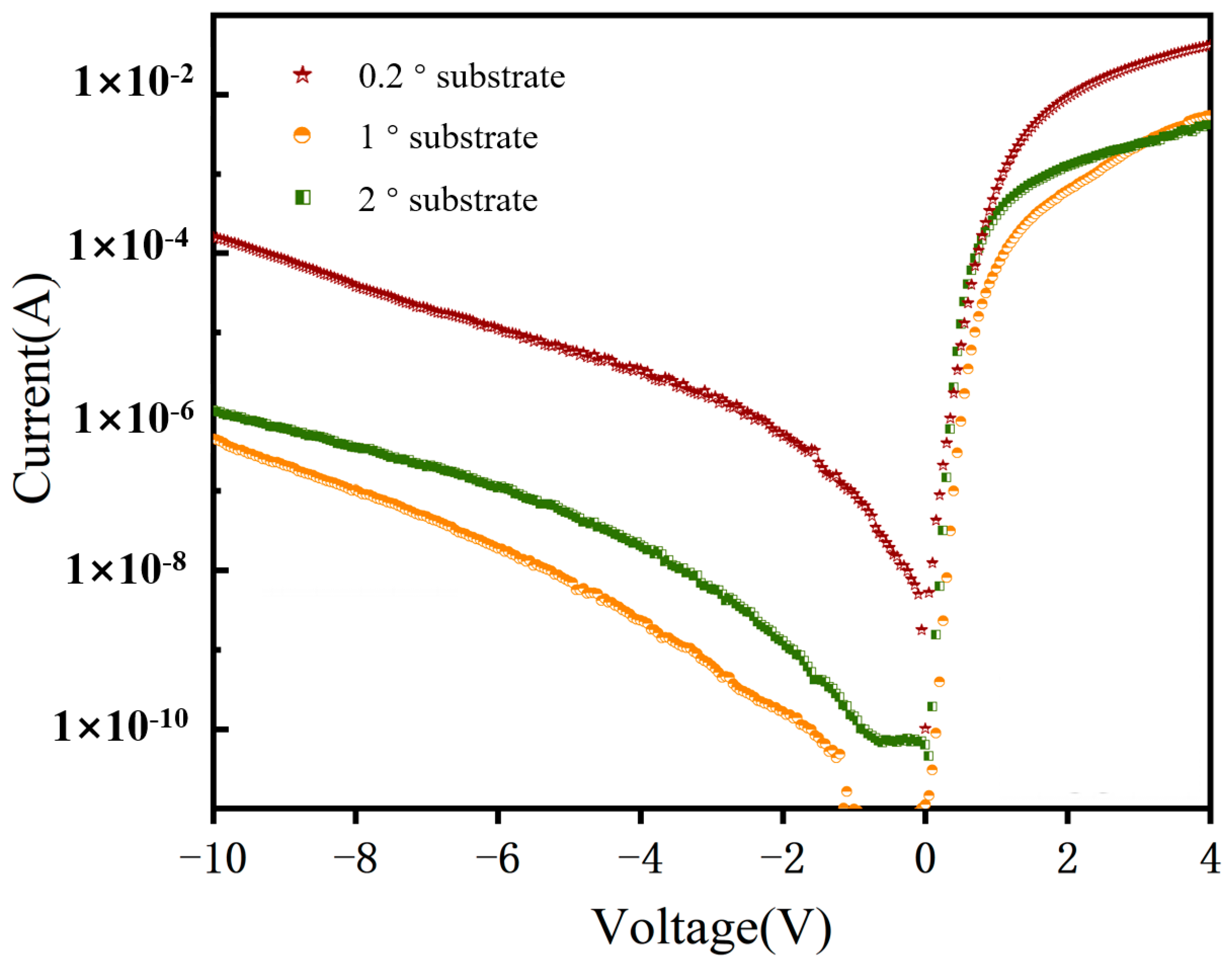
Based upon the surface morphology and our crystal quality investigations of N-polar GaN grown on different misoriented substrates, Figure 4 compares the I–V characteristics of the N-polar MIS Schottky barrier diode with different substrate orientations. Similar on-state resistance values are identified among all three samples, but there is a significant difference in the reverse-bias leakage current. The lowest reverse leakage in the sample fabricated on the 1° misoriented sapphire corresponds well with its smooth surface morphology and relatively better crystal quality compared to those of the other samples. This again verifies the hypothesis that N-polar GaN with a smooth surface morphology and good crystal quality is vital for uniform dielectric deposition and greatly reduced surface states, thus leading to significantly suppressed reverse-bias leakage current.
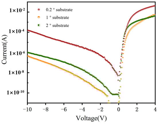
Figure 4.
I–V characteristics of N-polar GaN MIS Schottky barrier diode grown on different misoriented sapphire substrates.
Next, the Schottky barrier heights and ideality factors of above three samples were calculated and compared. The correlation between the voltage and the current in the Schottky diode is represented by Equations (4) and (5) below:
is the saturation current, is the contact area, is the effective Richardson constant, is the absolute temperature, is the Boltzmann constant, and is the applied voltage across the MIS-type structure. and the ideality factor, and is the ideality factor [45]. As shown in Table 2, the barrier heights of the MIS-type Schottky contacts are 0.5, 0.68, and 0.56 eV, respectively, for the N-polar GaN grown on the 0.2°, 1°, and 2° misoriented substrates. Corresponding values were also collected from the Ga-polar GaN samples. The ideality factor and barrier height are calculated to be 2.8 and 0.84 V, respectively. The Schottky barrier height and ideality factor values are consistent with those of other reports [46,47], even though lower ideality factors are obtained in the Schottky contact without the SiNx insertion layer. The reasons for this will be discussed later. A comparison between the values collected from the I–V characteristics and XPS analysis shown in Figure 3 reveals a large discrepancy. This could be caused by a lot of factors, including the high density of surface states that was not revealed by XPS and the tunneling effect [18]. In our work specifically, it is expected that traps inside the dielectric layer as well as the interface facilitate the carrier tunneling effect, and the heterostructure cannot be simply described by a thermionic emission model. A trap-assisted tunneling mechanism might partially contribute to the results and will be thoroughly investigated in the future. The ideality factors of all three samples are larger than 2. The exact reason for the observation of large ideality factors is not clear now. However, the doping concentration in the film was observed to be far higher than the Boltzmann doping limit; the distance between the conduction band and Fermi level was significantly lower than 3 kT. The traditionally used thermionic emission current model depicted in Equations (4) and (5) is valid when the Boltzmann condition is satisfied, which is as follows: [48]. Moreover, the N-polar GaN thin film used in this work shows a large surface roughness indicating possibilities of assisted tunneling conduction mechanisms, which will be discussed later. This will degrade the diode ideality factor [48,49]. Despite this, the highest Schottky barrier height of 0.68 eV and lowest ideality factor of 2.4 are obtained for the device grown on the 1° misoriented substrate, whose trend is in good agreement with the lowest leakage current of the corresponding device.
Table 2.
Schottky barrier heights and ideality factors calculated from I–V characteristics of MIS Schottky barrier diodes grown on sapphires with different misorientation angles.
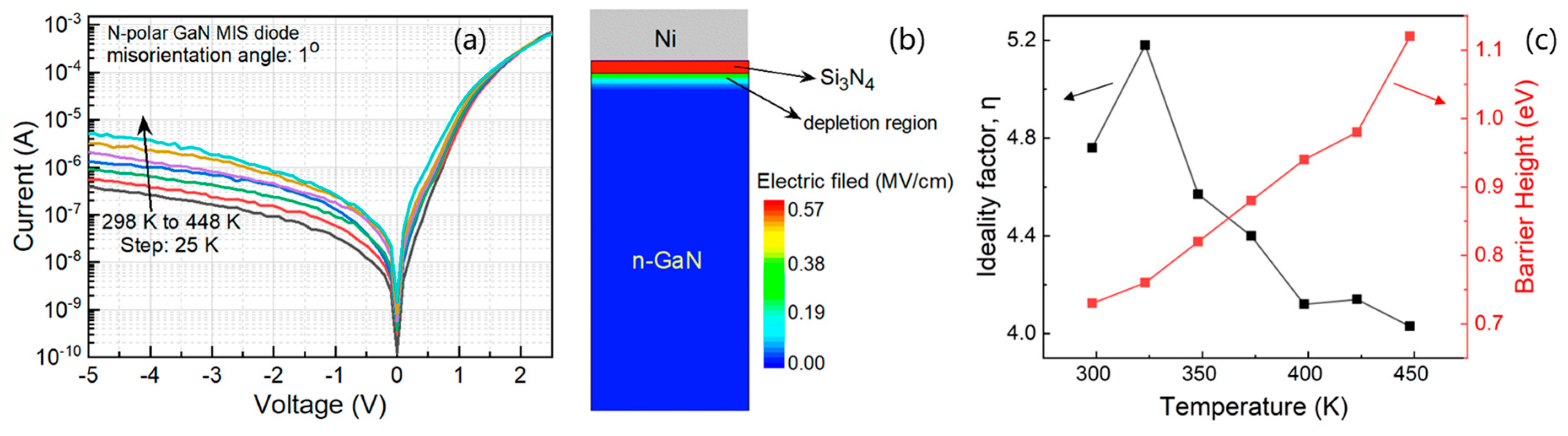
The possible cause of reverse leakage was investigated looking at the diodes’ temperature-dependent I–V characteristics and using TCAD simulations. For this, the MIS diode grown on the sapphire with a misorientation angle of 1° was investigated. Figure 5a shows the I–V characteristics of this diode when the temperature was varied from 298 K to 448 K in steps of 25 K. A gradual increase in the leakage current was observed with the increase in the temperature. Interestingly, the reverse leakage current increases by less than an order of magnitude under a −2 V reverse bias. In contrast, a previous report from Khachariya et al. suggests that a N-polar GaN MIS diode consisting of a Ni Schottky contact and a 5 nm LPCVD SiNx interlayer resulted in more than an order of magnitude increment in the leakage current at a similar voltage and for a similar temperature range [50]. Therefore, the interface with LPCVD SiNx is thought to represent incremental progress in this work compared to prior reports of the N-polar GaN MIS diode.
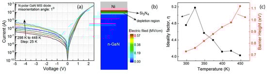
Figure 5.
(a) Temperature-dependent I–V characteristics of N-polar GaN MIS Schottky barrier diode with misorientation angle of 1°; (b) Electric field profile extracted from simulations; (c) Temperature-dependent ideality factor and Schottky barrier height of N-polar MIS Schottky barrier diode.
To further evaluate the leakage mechanism, TCAD simulations were performed to estimate the band bending under a −5 V reverse bias. For this, an MIS diode was simulated while considering Si3N4 as the insulator; parameters such as the doping concentration, energy bandgap, and barrier height were matched to their experimentally measured counterparts. To avoid edge effects, the Schottky contact was assumed to occupy the entire top surface, whereas the ohmic contact was assumed to occupy the entire bottom surface. The relative dielectric constants of GaN and SiNx were assumed to be ~10.4 and ~6.7, respectively. Both of these values were adopted from previously available reports [51,52]. Further details about the simulation setup and GaN-related parameters can be found elsewhere [53,54]. Unlike those under a forward bias, tunneling analyses under a reverse bias are suitable for a wider range of applied bias. The simulated electric field profile (at equilibrium) of the N-polar GaN MIS Schottky barrier diode is shown in Figure 5b. The SiNx layer was observed to have a significantly higher electric field compared to the n-GaN film. This is primarily caused by a significant difference in the dielectric constant and low thickness of the SiNx layer. Therefore, the electric field at the Ni/SiNx interface is expected to be large enough to promote assisted tunneling conduction during the reverse bias of the diode. Figure 5c illustrates the temperature-dependent barrier height and ideality factor of the N-polar MIS-type Schottky contact. An inverse correlation was established between the Schottky barrier height and ideality factor, consistent with previous reports [55,56]. Similarly, the graph showing the temperature-dependent barrier height and ideality factor of the Ga-polar Schottky contact was also illustrated in Figure S4.
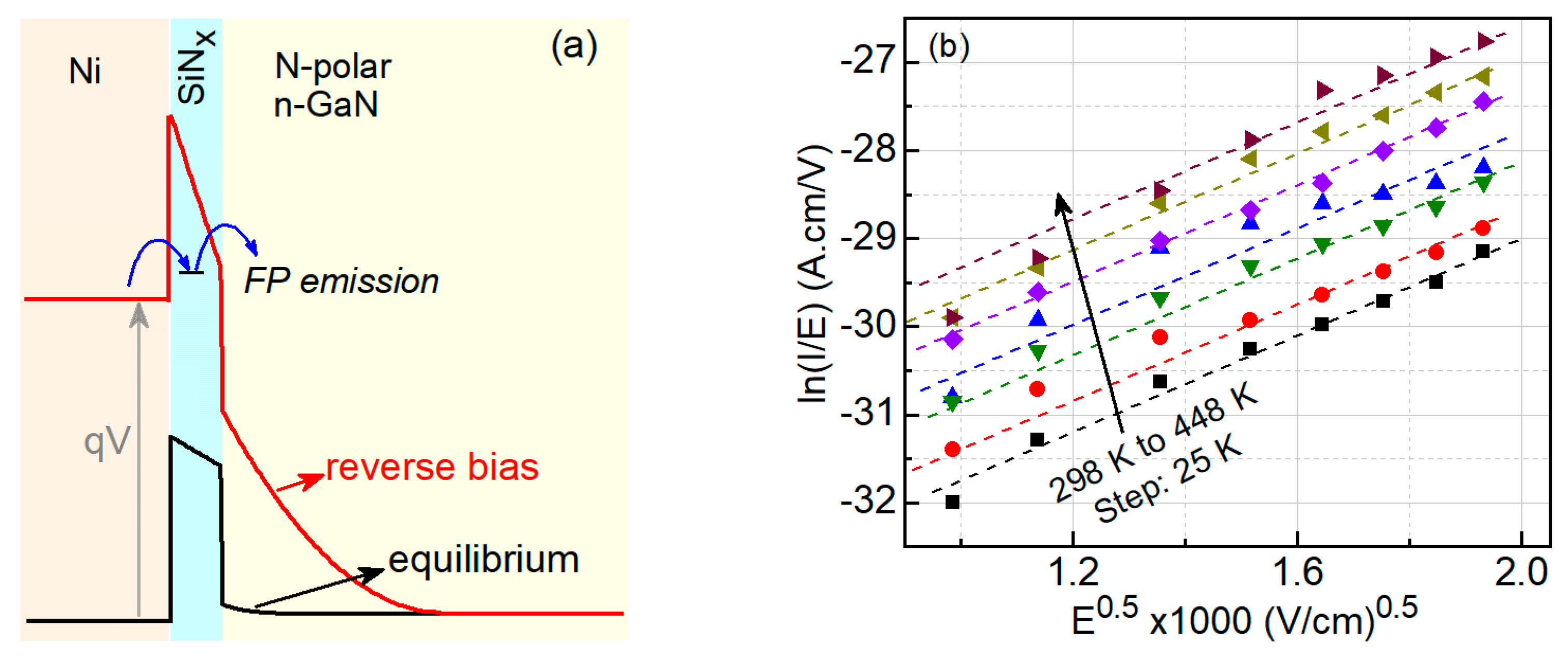
Moreover, a large band bending is also likely to result in a near-triangular barrier for the electrons to tunnel from Ni to n-GaN via the thin Si3N4 interlayer. For instance, a diagram of the energy band diagram of the N-polar GaN MIS diode at equilibrium and at a finite reverse voltage V is shown in Figure 6a. The large electric field inside the SiNx layer under reverse bias conditions induce significant band bending, as highlighted in Figure 6a. Thus, the presence of the interface/bulk traps in the SiNx layer can readily promote FP emission assisted current (IFPE) under reverse bias. To validate this hypothesis, an FP emission analysis of the reverse leakage current was performed. When the reverse leakage current is dominated by the FP emission mechanism, the value of IFPE is a function of E given by the following relation [57]:
where B1 is a proportionality constant, is the dielectric constant of the LPCVD SiNx layer, E is the electric field experienced by the carriers to undergo the tunneling process, is the electron trap energy, and q is the electronic charge. In such a scenario, a plot of ln(I/E) versus E0.5 is likely to yield straight lines for various temperatures. The plot of ln(I/E) versus E0.5 for the reverse I–V characteristics of the diode indeed yielded straight lines for every temperature, as observed in Figure 6b. From these observations, the FP emission is thought to be the dominant reverse conduction mechanism for the N-polar GaN MIS diode investigated in this work, as highlighted in Figure 6a. These trap states are also likely to promote tunneling currents during forward bias, thereby degrading the diode ideality factor, as observed in Table 2. Therefore, the optimization of the LPCVD SiNx film on the N-polar n-GaN with a modulated interface quality is necessary to further minimize the reverse leakage current. However, a significant reduction in the reverse leakage by the introduction of a thin LPCVD SiNx interlayer compared to a regular Ni/n-GaN Schottky diode shows a promising approach to realize highly efficient N-polar GaN MIS diodes for future high-power and high-speed electronic applications.
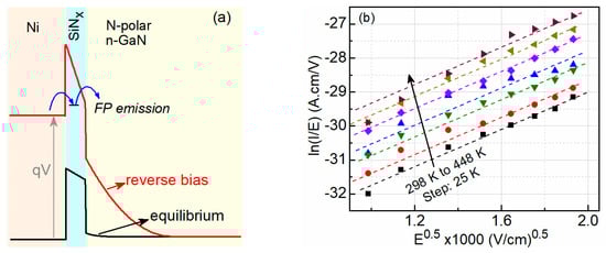
Figure 6.
(a) Diagram of the conduction band energy profile of the N-polar GaN MIS diode at equilibrium and at a reverse voltage V; (b) FP emission analysis of the reverse leakage current.
4. Conclusions
In summary, we have fabricated and characterized GaN-based MIS-type Schottky contacts with two opposite polarity surfaces. The N-polar Schottky contact shows a higher reverse-bias current compared to its Ga-polar counterpart but exhibits a lower on-state resistance. As calculated using an XPS characterization, the band offset at the N-polar GaN/SiNx interface is 1.65 eV, smaller than that of the Ga-polar GaN/SiNx heterojunction, which is 2.55 eV. The drastically different electrical behaviors and band profiles between the Ga- and N-polar Schottky contacts are attributed to the opposite spontaneous polarization fields and distinct surface morphologies of thin films with different polarities. To further understand the miscut angle on the performance of N-polar contacts, N-polar Schottky barrier diodes grown on 0.2, 1, and 2° misoriented substrates were prepared. A lower reverse-bias leakage current, higher on/off ratio, and lower ideality factor were achieved for the devices grown on the 1° misoriented substrate compared to the others, which also had the smoothest surface morphology and best crystal quality. Finally, the diode reverse leakage current was thought to be dominated by the Frenkel–Poole emission mechanism, which necessitates the further optimization of the insulator (SiNx) and/or interface quality. Overall, this work not only provides insight for the influence of thin film polarity on the electrical behaviors of MIS-type Schottky barrier diodes, but also highlights the importance of the surface and quality control of N-polar GaN in the development of GaN-based electronic devices. For the successful development of N-polar Schottky contacts, a smooth surface morphology, reduced defect density, and high-quality LPCVD SiNx passivation layers are desirable.
Supplementary Materials
The following supporting information can be downloaded at: https://www.mdpi.com/article/10.3390/electronics13091679/s1, Figure S1. Optical microscope image showing the distribution and density of the hillocks; Figure S2. Surface morphologies of N-polar GaN grown on 0.2°, 1° and 2° misoriented substrate; Figure S3. XRD (002) rocking curves of N-GaN grown on sapphire with various misorientation angles; Figure S4. Temperature-dependent ideality factor and barrier height of Ga-polar MIS Schottky barrier height.
Author Contributions
Conceptualization and investigation, Z.Y. and Y.D.; methodology, Z.Y. and S.Q.; validation, K.T. and T.L.; writing—original draft preparation, Z.Y.; Formal analysis: S.S. and B.S.; writing—review and editing, B.S. and W.G.; supervision, L.H.; project administration, W.G. and J.Y.; funding acquisition, L.H. and W.G. All authors have read and agreed to the published version of the manuscript.
Funding
This work was funded by National Natural Science Foundation of China (U21A20498), Youth Innovation Promotion Association of the Chinese Academy of Sciences (2020298), Key Research and Development Program of Ningbo City (2022Z086, 2022Z088, 2023Z072), and Shanghai Pujiang Programme (23PJD034).
Data Availability Statement
The data that support the findings of this study are available from the corresponding author upon reasonable request.
Conflicts of Interest
The authors declare no conflicts of interest. Author Shengli Qi was employed by the company Ningbo ANN Semiconductor Co., Ltd. The remaining authors declare that the research was conducted in the absence of any commercial or financial relationships that could be construed as a potential conflict of interest.
References
- Baliga, B.J. Gallium nitride devices for power electronic applications. Semicond. Sci. Technol. 2013, 28, 074011. [Google Scholar] [CrossRef]
- Amano, H.; Baines, Y.; Beam, E.; Borga, M.; Bouchet, T.; Chalker, P.R.; Charles, M.; Chen, K.J.; Chowdhury, N.; Chu, R.M.; et al. The 2018 GaN power electronics roadmap. J. Phys. D-Appl. Phys. 2018, 51, 163001. [Google Scholar] [CrossRef]
- Laurent, M.A.; Gupta, G.; Suntrup, D.J.; DenBaars, S.P.; Mishra, U.K. Barrier height inhomogeneity and its impact on (Al, In, Ga)N Schottky diodes. J. Appl. Phys. 2016, 119, 064501. [Google Scholar] [CrossRef]
- Kim, H. Vertical Schottky Contacts to Bulk GaN Single Crystals and Current Transport Mechanisms: A Review. J. Electron. Mater. 2021, 50, 6688–6707. [Google Scholar] [CrossRef]
- Fu, H.Q.; Fu, K.; Chowdhury, S.; Palacios, T.; Zhao, Y.J. Vertical GaN Power Devices: Device Principles and Fabrication Technologies—Part I. IEEE Trans. Electron Devices 2021, 68, 3200–3211. [Google Scholar] [CrossRef]
- Mönch, W. On the alleviation of Fermi-level pinning by ultrathin insulator layers in Schottky contacts. J. Appl. Phys. 2012, 111, 073706. [Google Scholar] [CrossRef]
- Yue, Y.Z.; Hao, Y.; Feng, Q.; Zhang, J.C.; Ma, X.H.; Ni, J.Y. GaN MOS-HEMT using ultra-thin Al2O3 dielectric grown by atomic layer deposition. Chin. Phys. Lett. 2007, 24, 2419–2422. [Google Scholar]
- He, J.B.; Hua, M.Y.; Zhang, Z.F.; Chen, K.J. Performance and VTH Stability in E-Mode GaN Fully Recessed MIS-FETs and Partially Recessed MIS-HEMTs with LPCVD-SiNx/PECVD-SiNxGate Dielectric Stack. IEEE Trans. Electron Devices 2018, 65, 3185–3191. [Google Scholar] [CrossRef]
- Cai, Y.T.; Zhang, Y.L.; Liang, Y.; Mitrovic, I.Z.; Wen, H.Q.; Liu, W.; Zhao, C.Z. Low ON-State Resistance Normally-OFF AlGaN/GaN MIS-HEMTs With Partially Recessed Gate and ZrOxCharge Trapping Layer. IEEE Trans. Electron Devices 2021, 68, 4310–4316. [Google Scholar] [CrossRef]
- Liu, C.; Chor, E.F.; Tan, L.S. Enhanced device performance of AlGaN/GaN HEMTs using HfO2 high-k dielectric for surface passivation and gate oxide. Semicond. Sci. Technol. 2007, 22, 522–527. [Google Scholar] [CrossRef]
- Keller, S.; Li, H.R.; Laurent, M.; Hu, Y.L.; Pfaff, N.; Lu, J.; Brown, D.F.; Fichtenbaum, N.A.; Speck, J.S.; DenBaars, S.P.; et al. Recent progress in metal-organic chemical vapor deposition of (000(1)over-bar) N-polar group-III nitrides. Semicond. Sci. Technol. 2014, 29, 113001. [Google Scholar] [CrossRef]
- Dai, Y.J.; Guo, W.; Chen, L.; Xu, H.Q.; AlQatari, F.; Guo, C.Y.; Peng, X.C.; Tang, K.; Liao, C.H.; Li, X.H.; et al. Polarization modulation of 2DEG toward plasma-damage-free GaN HEMT isolation. Appl. Phys. Lett. 2022, 121, 012104. [Google Scholar] [CrossRef]
- Dasgupta, S.; Nidhi; Brown, D.F.; Wu, F.; Keller, S.; Speck, J.S.; Mishra, U.K. Ultralow nonalloyed Ohmic contact resistance to self aligned N-polar GaN high electron mobility transistors by In(Ga)N regrowth. Appl. Phys. Lett. 2010, 96, 143504. [Google Scholar] [CrossRef]
- Sheikhi, M.; Li, J.M.; Meng, F.P.; Li, H.W.; Guo, S.P.; Liang, L.Y.; Cao, H.T.; Gao, P.Q.; Ye, J.C.; Guo, W. Polarity Control of GaN and Realization of GaN Schottky Barrier Diode Based on Lateral Polarity Structure. IEEE Trans. Electron Devices 2017, 64, 4424–4429. [Google Scholar] [CrossRef]
- Hatui, N.; Krishna, A.; Li, H.; Gupta, C.; Romanczyk, B.; Acker-James, D.; Ahmadi, E.; Keller, S.; Mishra, U.K. Ultra-high silicon doped N-polar GaN contact layers grown by metal-organic chemical vapor deposition. Semicond. Sci. Technol. 2020, 35, 095002. [Google Scholar] [CrossRef]
- Lu, J.; Zheng, X.; Guidry, M.; Denninghoff, D.; Ahmadi, E.; Lal, S.; Keller, S.; DenBaars, S.P.; Mishra, U.K. Engineering the (In, Al, Ga)N back-barrier to achieve high channel-conductivity for extremely scaled channel-thicknesses in N-polar GaN high-electron-mobility-transistors. Appl. Phys. Lett. 2014, 104, 092107. [Google Scholar] [CrossRef]
- Suemitsu, T.; Makabe, I. Effective Schottky Barrier Height Model for N-Polar and Ga-Polar GaN by Polarization-Induced Surface Charges with Finite Thickness. Phys. Status Solidi B—Basic Solid State Phys. 2020, 257, 1900528. [Google Scholar] [CrossRef]
- Khachariya, D.; Szymanski, D.; Sengupta, R.; Reddy, P.; Kohn, E.; Sitar, Z.; Collazo, R.; Pavlidis, S. Chemical treatment effects on Schottky contacts to metalorganic chemical vapor deposited n-type N-polar GaN. J. Appl. Phys. 2020, 128, 064501. [Google Scholar] [CrossRef]
- Reddy, P.; Bryan, I.; Bryan, Z.; Guo, W.; Hussey, L.; Collazo, R.; Sitar, Z. The effect of polarity and surface states on the Fermi level at III-nitride surfaces. J. Appl. Phys. 2014, 116, 123701. [Google Scholar] [CrossRef]
- Liu, Z.X.; Wu, Q.S.; Wang, Y.P.; Qiu, Q.L.; Zhang, J.W.; Wu, Z.S.; Liu, Y. Mechanism of high conduction on the N polar face of GaN. J. Appl. Phys. 2022, 131, 235701. [Google Scholar] [CrossRef]
- Hu, J.; Nainani, A.; Sun, Y.; Saraswat, K.C.; Wong, H.S.P. Impact of fixed charge on metal-insulator-semiconductor barrier height reduction. Appl. Phys. Lett. 2011, 99, 252104. [Google Scholar] [CrossRef]
- Li, Y.; Hu, X.; Song, Y.; Su, Z.; Wang, W.; Jia, H.; Wang, W.; Jiang, Y.; Chen, H. The role of AlN thickness in MOCVD growth of N-polar GaN. J. Alloys Compd. 2021, 884, 161134. [Google Scholar] [CrossRef]
- Jiang, J.; Zhang, Y.; Yang, F.; Huang, Z.; Yan, L.; Li, P.; Chi, C.; Zhao, D.; Zhang, B.; Du, G. Study of N-polar GaN growth with a high resistivity by metal-organic chemical vapor deposition. Vacuum 2015, 119, 63–67. [Google Scholar] [CrossRef]
- Li, C.G.; Zhang, K.; Zeng, Q.Y.; Wang, Q.; Li, Z.L.; Zhao, W.; Chen, Z.T. Effect of V/III ratio on the surface morphologies of N-polar GaN films grown on offcut sapphire substrates. J. Cryst. Growth 2020, 536, 125599. [Google Scholar] [CrossRef]
- Keller, S.; Fichtenbaum, N.; Wu, F.; Brown, D.; Rosales, A.; DenBaars, S.; Speck, J.; Mishra, U. Influence of the substrate misorientation on the properties of N-polar GaN films grown by metal organic chemical vapor deposition. J. Appl. Phys. 2007, 102, 083546. [Google Scholar] [CrossRef]
- Mohanty, S.; Sayed, I.; Jian, Z.A.; Mishra, U.; Ahmadi, E. Investigation and optimization of HfO2 gate dielectric on N-polar GaN: Impact of surface treatments, deposition, and annealing conditions. Appl. Phys. Lett. 2021, 119, 042901. [Google Scholar] [CrossRef]
- Guo, W.; Xu, H.Q.; Chen, L.; Yu, H.B.; Jiang, J.A.; Sheikhi, M.; Li, L.; Dai, Y.J.; Cui, M.; Sun, H.D.; et al. Polarity control and fabrication of lateral polarity structures of III-nitride thin films and devices: Progress and prospects. J. Phys. D—Appl. Phys. 2020, 53, 483002. [Google Scholar] [CrossRef]
- Guo, W.; Sun, H.D.; Torre, B.; Li, J.M.; Sheikhi, M.; Jiang, J.A.; Li, H.W.; Guo, S.P.; Li, K.H.; Lin, R.H.; et al. Lateral-Polarity Structure of AlGaN Quantum Wells: A Promising Approach to Enhancing the Ultraviolet Luminescence. Adv. Funct. Mater. 2018, 28, 1802395. [Google Scholar] [CrossRef]
- Mita, S.; Collazo, R.; Rice, A.; Tweedie, J.; Xie, J.Q.; Dalmau, R.; Sitar, Z. Impact of gallium supersaturation on the growth of N-polar GaN. In Proceedings of the International Workshop on Nitride Semiconductors (IWN)/Fall Meeting of the European-Materials-Research-Society (E-MRS)/Symposium N/Symposium H, Tampa, FL, USA, 19–24 September 2010. [Google Scholar]
- Wang, H.-C.; Lumbantoruan, F.J.; Hsieh, T.-E.; Wu, C.-H.; Lin, Y.-C.; Chang, E.Y. High-Performance LPCVD-SiN x/InAlGaN/GaN MIS-HEMTs With 850-V 0.98 mΩ·cm 2 for Power Device Applications. IEEE J. Electron Devices Soc. 2018, 6, 1136–1141. [Google Scholar] [CrossRef]
- Jing, G.J.; Wang, X.H.; Huang, S.; Jiang, Q.M.; Deng, K.X.; Wang, Y.H.; Li, Y.K.; Fan, J.; Wei, K.; Liu, X.Y. Mechanism of Linearity Improvement in GaN HEMTs by Low Pressure Chemical Vapor Deposition-SiNx Passivation. IEEE Trans. Electron Devices 2022, 69, 6610–6615. [Google Scholar] [CrossRef]
- Boulard, F.; Gros, V.; Porzier, C.; Brunet, L.; Lapras, V.; Fournel, F.; Truffier-Boutry, D.; Autillo, D.; Ruault, P.; Keovisai, M.; et al. Bevel contamination management in 3D integration by localized SiO2 deposition. Microelectron. Eng. 2022, 265, 111875. [Google Scholar] [CrossRef]
- Nomoto, K.; Xing, H.G.; Jena, D.; Cho, Y. N-polar GaN pn junction diodes with low ideality factors. Appl. Phys. Express 2022, 15, 064004. [Google Scholar] [CrossRef]
- Li, Y.; Wang, M.; Yin, R.; Zhang, J.; Tao, M.; Xie, B.; Hao, Y.; Yang, X.; Wen, C.P.; Shen, B. Quasi-vertical GaN Schottky barrier diode on silicon substrate with 10 10 high on/off current ratio and low specific on-resistance. IEEE Electron Device Lett. 2020, 41, 329–332. [Google Scholar] [CrossRef]
- Reddy, P.; Washiyama, S.; Kaess, F.; Breckenridge, M.H.; Hernandez-Balderrama, L.H.; Haidet, B.B.; Alden, D.; Franke, A.; Sarkar, B.; Kohn, E.; et al. High temperature and low pressure chemical vapor deposition of silicon nitride on AlGaN: Band offsets and passivation studies. J. Appl. Phys. 2016, 119, 145702. [Google Scholar] [CrossRef]
- Eller, B.S.; Yang, J.L.; Nemanich, R.J. Electronic surface and dielectric interface states on GaN and AlGaN. J. Vac. Sci. Technol. A 2013, 31, 050807. [Google Scholar] [CrossRef]
- Khachariya, D.; Szymanski, D.; Breckenridge, M.H.; Reddy, P.; Kohn, E.; Sitar, Z.; Collazo, R.; Pavlidis, S. On the characteristics of N-polar GaN Schottky barrier contacts with LPCVD SiN interlayers. Appl. Phys. Lett. 2021, 118, 122103. [Google Scholar] [CrossRef]
- Reddy, P.; Khachariya, D.; Szymanski, D.; Breckenridge, M.H.; Sarkar, B.; Pavlidis, S.; Collazo, R.; Sitar, Z.; Kohn, E. Role of polarity in SiN on Al/GaN and the pathway to stable contacts. Semicond. Sci. Technol. 2020, 35, 055007. [Google Scholar] [CrossRef]
- Zhang, S.; Wei, K.; Xiao, Y.; Ma, X.H.; Zhang, C.; Liu, G.G.; Lei, T.M.; Zheng, Y.K.; Huang, S.; Wang, N.; et al. Effect of SiN:Hx passivation layer on the reverse gate leakage current in GaN HEMTs. Chin. Phys. B 2018, 27, 097309. [Google Scholar] [CrossRef]
- Luo, B.; Johnson, J.W.; Ren, F.; Baik, K.W.; Pearton, S.J. Effect of plasma enhanced chemical vapor deposition of SiNx on n-GaN Schottky rectifiers. Solid-State Electron. 2002, 46, 705–710. [Google Scholar] [CrossRef]
- Hu, X.T.; Song, Y.M.; Su, Z.L.; Jia, H.Q.; Wang, W.X.; Jiang, Y.; Li, Y.F.; Chen, H. Characterization of the N-polar GaN film grown on C-plane sapphire and misoriented C-plane sapphire substrates by MOCVD. Chin. Phys. B 2022, 31, 038103. [Google Scholar] [CrossRef]
- Bryan, I.; Bryan, Z.; Mita, S.; Rice, A.; Tweedie, J.; Collazo, R.; Sitar, Z. Surface kinetics in AlN growth: A universal model for the control of surface morphology in III-nitrides. J. Cryst. Growth 2016, 438, 81–89. [Google Scholar] [CrossRef]
- Marini, J.; Leathersich, J.; Mahaboob, I.; Bulmer, J.; Newman, N.; Shahedipour-Sandvik, F.S. MOCVD growth of N-polar GaN on on-axis sapphire substrate: Impact of AlN nucleation layer on GaN surface hillock density. J. Cryst. Growth 2016, 442, 25–30. [Google Scholar] [CrossRef]
- Kim, H. Effect of KOH treatment on the Schottky barrier inhomogeneity in Ni/n-GaN. Mater. Sci. Semicond. Process 2010, 13, 51–55. [Google Scholar] [CrossRef]
- Isobe, K.; Akazawa, M. Impact of surface treatment on metal-work-function dependence of barrier height of GaN-on-GaN Schottky barrier diode. AIP Adv. 2018, 8, 115011. [Google Scholar] [CrossRef]
- Lakshmi, B.P.; Reddy, M.S.P.; Kumar, A.A.; Reddy, V.R. Electrical transport properties of Au/SiO2/n-GaN MIS structure in a wide temperature range. Curr. Appl. Phys. 2012, 12, 765–772. [Google Scholar] [CrossRef]
- Xu, N.; Deng, G.; Ma, H.; Yang, S.; Niu, Y.; Yu, J.; Wang, Y.; Zhao, J.; Zhang, Y. Effect of annealing on the electrical performance of N-polarity GaN Schottky barrier diodes. J. Semicond. 2024, 45, 042501. [Google Scholar] [CrossRef]
- Mukhopadhyay, S.; Lyle, L.A.; Pal, H.; Das, K.K.; Porter, L.M.; Sarkar, B. Evidence of thermionic emission in forward biased β-Ga2O3 Schottky diodes at Boltzmann doping limit. J. Appl. Phys. 2022, 131, 025702. [Google Scholar] [CrossRef]
- Zhang, T.; Zhang, Y.; Zhang, J.; Li, X.; Lv, Y.; Hao, Y. Current transport mechanism of high-performance novel GaN MIS diode. IEEE Electron Device Lett. 2021, 42, 304–307. [Google Scholar] [CrossRef]
- Khachariya, D.; Szymanski, D.; Reddy, P.; Kohn, E.; Sitar, Z.; Collazo, R.; Pavlidis, S. Schottky contacts to N-polar GaN with SiN interlayer for elevated temperature operation. Appl. Phys. Lett. 2022, 120, 172109. [Google Scholar] [CrossRef]
- Suda, J.; Yamaji, K.; Hayashi, Y.; Kimoto, T.; Shimoyama, K.; Namita, H.; Nagao, S. Nearly ideal current–voltage characteristics of Schottky barrier diodes formed on hydride-vapor-phase-epitaxy-grown GaN free-standing substrates. Appl. Phys. Express 2010, 3, 101003. [Google Scholar] [CrossRef]
- Qi, Y.; Zhu, Y.; Zhang, J.; Lin, X.; Cheng, K.; Jiang, L.; Yu, H. Evaluation of LPCVD SiN x gate dielectric reliability by TDDB measurement in Si-substrate-based AlGaN/GaN MIS-HEMT. IEEE Trans. Electron Devices 2018, 65, 1759–1764. [Google Scholar] [CrossRef]
- Patel, J.; Pramanik, T.; Sarkar, B. Analytical Model of Center Potential in GaN Vertical Junctionless Power Fin-MOSFETs for Fast Device-Design Optimization. IEEE Trans. Electron Devices 2023, 71, 99–106. [Google Scholar] [CrossRef]
- Pal, H.; Singh, S.; Guo, C.; Guo, W.; Badami, O.; Pramanik, T.; Sarkar, B. Lateral P–N Junction Photodiodes Using Lateral Polarity Structure GaN Films: A Theoretical Perspective. J. Electron. Mater. 2023, 52, 2148–2157. [Google Scholar] [CrossRef]
- Schmitsdorf, R.; Kampen, T.; Mönch, W. Explanation of the linear correlation between barrier heights and ideality factors of real metal-semiconductor contacts by laterally nonuniform Schottky barriers. J. Vac. Sci. Technol. B Microelectron. Nanometer Struct. Process. Meas. Phenom. 1997, 15, 1221–1226. [Google Scholar] [CrossRef]
- Kumar, A.; Kapoor, R.; Garg, M.; Kumar, V.; Singh, R. Direct evidence of barrier inhomogeneities at metal/AlGaN/GaN interfaces using nanoscopic electrical characterizations. Nanotechnology 2017, 28, 26LT02. [Google Scholar] [CrossRef] [PubMed]
- Mukherjee, A.; Vasquez, J.M.T.; Ashai, A.; Yuvaraja, S.; Rajbhar, M.; Sarkar, B.; Li, X. On band-to-band tunneling and field management in NiOx/β-Ga2O3 PN junction and PiN diodes. J. Phys. D Appl. Phys. 2023, 56, 475104. [Google Scholar] [CrossRef]

Disclaimer/Publisher’s Note: The statements, opinions and data contained in all publications are solely those of the individual author(s) and contributor(s) and not of MDPI and/or the editor(s). MDPI and/or the editor(s) disclaim responsibility for any injury to people or property resulting from any ideas, methods, instructions or products referred to in the content. |
© 2024 by the authors. Licensee MDPI, Basel, Switzerland. This article is an open access article distributed under the terms and conditions of the Creative Commons Attribution (CC BY) license (https://creativecommons.org/licenses/by/4.0/).