Article

Self-Switching Wireless Power Transfer System Design with Constant Current/Constant Voltage Output Features Based on LCC-LCL/S Topology

1
Hubei Engineering Research Center for Safety Monitoring of New Energy and Power Grid Equipment, Hubei University of Technology, Wuhan 430068, China
2
School of Electrical and Electronic Engineering, Hubei University of Technology, Wuhan 430068, China
3
School of Information Science and Engineering, East China University of Science and Technology, Shanghai 200237, China
*
Author to whom correspondence should be addressed.
Electronics 2024, 13(9), 1729; https://doi.org/10.3390/electronics13091729
Submission received: 18 March 2024 / Revised: 22 April 2024 / Accepted: 28 April 2024 / Published: 30 April 2024

Abstract

:
To meet the demand for constant current and constant voltage charging of batteries and to increase the system output power, the LCC-LCL/S-type self-switching wireless power transfer system is proposed. The system does not require communication between the primary and secondary circuits, and its output mode is controlled by simply changing the status of two switches on the secondary side. Notably, the system satisfies the zero phase angle characteristic before and after mode switching. The parameter design method is proposed based on the circuit topology and the maximum safe current constraint. To make the output voltage fluctuation as small as possible, the optimum load switching point for the system has been designed, and its optimality has been validated by simulation. Furthermore, the switching control strategy is proposed, considering the effects of the system no-load and load short-circuit in real situations. Finally, an experimental platform was built to achieve the high efficiency output of the system with the maximum output voltage of 46.21 V, the maximum output power of 180 W, and the maximum efficiency of 93.4%, which verified the applicability of the proposed method.

1. Introduction

Wireless power transfer (WPT), a contactless power transmission technology, is free from traditional physical media constraints. It uses electromagnetic waves as the energy carrier and transmits power from the transmitting end to the receiving end to supply energy to the load [1], avoiding the safety issues caused by insulation damage, line aging, and tip discharging in traditional power transmission [2]. As a result, it has a wide range of applications, including electric vehicles [1,3,4,5], autonomous underwater vehicles [6,7], medical devices [8,9], smart positioning [10,11,12], and industry [13].
Lithium batteries have emerged as the preferred power source for modern electric equipment due to their excellent energy efficiency [14], and the safety of the charging process is critical. To reduce the safety issues associated with repeated plugging and unplugging, researchers are currently focusing on WPT technology for lithium battery charging [15]. The charging stages of lithium batteries mainly consist of constant current (CC) and constant voltage (CV) [16]. As the charging progresses, its resistance gradually increases due to alterations in the electrolyte concentration. Combined with the charging characteristics of lithium batteries, the design objective of the wireless charging system for lithium batteries is to achieve CC and CV output and switching and to ensure that voltage and current fluctuations are minimized at the moment of switching [17].
Presently, researchers are putting forth control strategies capable of achieving transitions between CC and CV in WPT systems. The three most common control methods are the introduction of power converters, system frequency control, and switching tube phase control. Refs. [18,19,20,21] added AC-AC or DC-DC converters for constant output. The system can collect real-time voltage and current data from the receiving end and uses them as feedback signals to control the converter for stable CC and CV output. Although the method has the advantages of system stability and fast response, the introduction of the converter increases the size and design cost of the receiver side. Refs. [22,23,24] realized the switching of the charging state by adjusting the frequency according to the characteristic of resonant circuits across various operating frequency points. However, frequency hopping control may cause frequency splitting, which influences the system operation stability. Ref. [25] used the method of phase shift control. At a constant frequency, the phase of the inverter switching tube is controlled based on feedback from sampled values. The scheme involves communication, and the switching strategy is complex.
To make up for the shortcomings of the control strategy, researchers have started to investigate how to optimize the compensation topology. Ref. [26] proposed a modelling method on the basis of the high-order resonance network. The hybrid topology with LCC and LCV modes was presented. Ref. [27] compounded the LCL-S-type topology with the bilateral LCL-P-type topology and realized the mode switching by changing the compensation capacitor, but the system did not satisfy the zero phase angle (ZPA) characteristic. Ref. [28] proposed either SS and PS compensation or SP and PP compensation with three switches to convert output modes. However, there will be a voltage spike across the switch, even damaging the switch, when it is closed with residual energy in the inductor. Ref. [29] proposed a reconfigurable wireless power transfer system with 3-D misalignment tolerance. However, the system had many coils and compensation components and a large device size, which increased the design and application costs. Ref. [30] split the intermediate coil into two coils and overlapped them with the receiving coil to create a compact structure. Although the charging mode can be switched during the charging process, the number of components and switches significantly increased the cost and the space requirements. Ref. [31] configured four relays to achieve the charging mode transition by controlling the pertinent pair of relays. However, the number of relays involved in the system is high, resulting in switching losses.
In summary, the current methods of CC/CV charging based on wireless power transfer technology can be roughly divided into two categories: one focuses on optimizing the control strategy; the other focuses on optimizing the topology. Compared with the latter, the former often involves bilateral communication and is limited by the application space and cost. Therefore, to reduce the control complexity and the system size as much as possible, based on the study of the output characteristics of the second-order and high-order compensation networks, this paper innovatively proposes an LCC-LCL/S compensation topology. It consists of the LCC-LCL-type network and the LCC-S-type network, which can be reconfigured by controlling the switches to achieve the switching of charging modes. The design schemes of system parameters and the optimal switching point are proposed based on theoretical derivation. The switching flow of the switches is given according to the analysis of the no-load and short-circuit conditions of the system, which lays the theoretical foundation for realizing efficient and stable operation.
The rest of the paper is divided into five sections. The first section analyses and verifies the output constant characteristic and the ZPA characteristic of the single topology; the second section proposes the parameter design method; the third section designs the optimal load switching point and proposes the switching control strategy; the fourth section carries out the simulation and experiment to prove the correctness of the proposed method. The last section is the conclusion of the paper.

2. System Topology Analysis

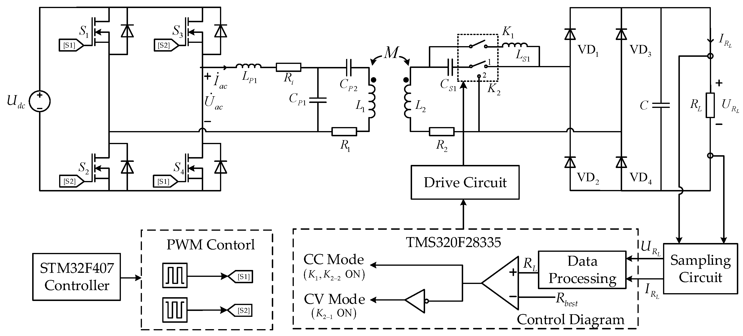
The self-switching of CC and CV characteristics cannot be finished by using a single compensation topology, which cannot meet the charging requirements of lithium batteries. Therefore, to better match the charging characteristics of lithium batteries, this paper combines the second-order S-type network with CV output characteristics and the third-order LCL-type network with CC output characteristics and proposes an output mode self-switching WPT system on the basis of the LCC-LCL/S compensation network. The system circuit is shown in Figure 1.
U d c is the DC power supply voltage; the input side circuit adopts a high-frequency full-bridge inverter circuit driven by MOSFETs; S 1 , S 2 and S 3 , S 4 form the bridge arms, respectively; L P 1 , C P 1 , C P 2 constitute the primary end LCC-type compensation network; L 1 , L 2 are primary and secondary coils self-inductance, respectively; R i is the internal resistance of L P 1 ; R 1 , R 2 are the internal resistance of coils, respectively; M represents coupled mutual inductance; L 2 , C S 1 , L S 1 form a secondary LCL-type compensation network, L 2 , C S 1 form a secondary S-type compensation network, and the compensation network is switched by controlling K 1 , K 2 ; an uncontrolled rectifier circuit driven by the diode is adopted, V D 1 , V D 2 and V D 3 , V D 4 form the bridge arms, respectively; C is the filter capacitor; R e q is the equivalent resistance of the rectifier circuit, the filter circuit, and the load; R L is the resistance of the load; U R L , I R L are the load voltage and current.
As mentioned in Ref. [32], as long as the port impedance of the loop is purely resistive, the current stress in the loop can be reduced. In this case, the system is in resonance, and its transmission efficiency is significantly improved. To increase the system’s output efficiency, it is necessary to investigate the resonance frequency in CC/CV mode. The output characteristics of the LCC-LCL-type and LCC-S-type circuit topologies and the system resonant frequency are analyzed in the following two subsections to prove the correctness of the mentioned compensation topology. Let the system operating frequency be ω .

2.1. LCC-LCL Topology Analysis

When the switch K 1 is closed and the switch K 2 is in contact with point two, the system is in CC output mode. Figure 2 shows the system equivalent mutual inductance circuit, where, U ˙ a c and I ˙ a c represent the input alternating voltage and current. L P 1 , C P 1 , C P 2 and L S 1 , C S 1 , L 2 constitute the primary and secondary resonant networks, respectively. R e q is the equivalent resistance, and U ˙ o , I ˙ o represent its voltage and current, respectively. I ˙ 1 , I ˙ 2 represent the current of coils, respectively. U ˙ a c , I ˙ a c , I ˙ 1 ,   I ˙ 2 , U ˙ o and I ˙ o indicate the phasors of corresponding variables, respectively. Furthermore, U a c , I a c , I 1 , I 2 , U o and I o are defined as the corresponding root-mean-square (rms) values, respectively.
Let the resonant frequency of the LCC-LCL-type topology be ω C C . Without considering mutual inductance M, the impedance Z C C 1 of the input side circuit satisfies the following equation:
Z C C 1 = Z C P 1 ( Z C P 2 + Z L 1 + R 1 ) Z C P 1 + Z C P 2 + Z L 1 + R 1 + Z L P 1 + R i
where Z L P 1 , Z C P 1 , Z L 1 , Z C P 2 are the impedance of each compensation component.
Let the imaginary part of the Z C C 1 be zero; at this time, the primary compensation circuit is in resonance, and its resonant frequency ω C C satisfies the following equations:
{ Z L P 1 + Z C P 1 = j ω C C L P 1 + 1 j ω C C C P 1 = 0 Z L 1 Z L P 1 + Z C P 2 = j ω C C ( L 1 L P 1 ) + 1 j ω C C C P 2 = 0
Without considering mutual inductance M, the impedance Z C C 2 of the output side circuit satisfies the following equation:
Z C C 2 = Z L 2 + R 2 + Z C S 1 ( Z L S 1 + R e q ) Z L S 1 + Z C S 1 + R e q
where Z L 2 , Z C S 1 , Z L S 1 are the impedance of each compensation component.
Let the imaginary part of the Z C C 2 be zero. The secondary compensation circuit is in resonance, and its resonant frequency ω C C satisfies the following equations:
{ Z L 2 + Z C S 1 = j ω C C L 2 + 1 j ω C C C S 1 = 0 Z L S 1 + Z C S 1 = j ω C C L S 1 + 1 j ω C C C S 1 = 0
To maximize efficiency, the system operating frequency should be equal to the resonant frequency, i.e., ω = ω C C . The secondary impedance in CC mode satisfies the following equation:
Z C C 2 = ( ω L S 1 ) 2 R e q + R 2
The impedance Z C C f from the secondary side equivalent to the primary side is
Z C C f = ( ω M ) 2 Z C C 2 = ω 2 M 2 R e q ω 2 L S 1 2 + R 2 R e q
To achieve full resonance of the circuit, the mutual inductance M is adjusted to meet the maximum power transfer theorem after the resonance has been realized in the circuit itself. Let the real part of the primary impedance be equal to the real part of the equivalent impedance from the secondary to the primary. The optimum mutual inductance resistance M o p t satisfies the following equation:
M o p t = ( 1 + ω 2 C P 1 2 R 1 R i ) ( ω 2 L S 1 2 + R 2 R e q ) ω 4 C P 1 2 R e q R 1
The primary input equivalent impedance Z C C I N satisfies the following equation:
Z C C I N = Z L P 1 + R i + Z C P 1 / / ( Z C P 2 + Z L 1 + R 1 + Z C C f ) = ( L 1 C P 2 ω 2 1 ) A + R i ω 2 C P 1 C P 2 ( ω 2 M 2 R e q + R 1 A ) ω 2 C P 1 C P 2 ( ω 2 M 2 R e q + R 1 A )
where A = ω 2 L S 1 2 + R 2 R e q .
Based on Kirchhoff’s law analysis, the following equations are obtained to solve for the magnitude of the system output values:
{ j ω M I ˙ C C 1 + ( j ω L 2 + 1 j ω C S 1 + R 2 ) I ˙ C C 2 1 j ω C S 1 I ˙ C C o = 0 ( j ω L P 1 + 1 j ω C P 1 + R i ) I ˙ a c 1 j ω C P 1 I ˙ C C 1 = U ˙ a c 1 j ω C S 1 I ˙ C C 2 + ( j ω L S 1 + 1 j ω C S 1 + R e q ) I ˙ C C o = 0 j ω M I ˙ C C 2 + ( 1 j ω C P 2 + j ω L 2 + R 1 ) I ˙ C C 1 = ( I ˙ a c I ˙ C C 1 ) 1 j ω C P 1
According to the relationship between the components of the system under resonance conditions, the primary coil current I ˙ C C 1 and the output current I ˙ C C o meet the following equation, respectively:
I ˙ C C 1 = j ω C P 1 U ˙ a c C B R i C
I ˙ C C o = j ω 3 M C P 1 C S 1 U ˙ a c B R i C
where { B = ω 4 ( C P 1 C S 1 ) 2 R 1 R 2 R e q ( ω C P 1 ) 2 R 1 C = ( ω C S 1 ) 2 R 2 R e q + 1 .
Based on Equation (8), the input and output power for the WPT system in the CC state satisfy the following equation, respectively:
P C C I N = | U ˙ a c | 2 Z C C I N = U a c 2 ω 2 C P 1 C P 2 ( ω 2 M 2 R e q + R 1 A ) ˙ ( L 1 C P 2 ω 2 1 ) A + R i ω 2 C P 1 C P 2 ( ω 2 M 2 R e q + R 1 A )
P C C O U T = | I ˙ C C o | 2 R e q = ω 6 M 2 C P 1 2 C S 1 2 U a c 2 ( B R i C ) 2 R e q
The system output efficiency in the CC mode satisfies the following equation:
η C C = P C C O U T P C C O U T = ω 6 M 2 C P 1 2 C S 1 2 U a c 2 R e q ( B R i C ) 2 ( ( L 1 C P 2 ω 2 1 ) A ˙ U a c 2 ω 2 C P 1 C P 2 ( ω 2 M 2 R e q + R 1 A ) + R i U a c 2 )
The internal resistance of the Litz wire coil is usually on the order of milliohms [33], which is at least two or more orders of magnitude different from the load resistance, so the internal resistance of the coil can be ignored. The compensation inductance L P 1 satisfies the equation R i ω L P 1 , so its parasitic internal resistance R i is also negligible. The system output current I ˙ C C o satisfies the equation:
I ˙ C C o = j ω 3 C P 1 C S 1 M U ˙ a c = M U ˙ a c j ω L P 1 L S 1
From the above equation, we can see that when the system satisfies the equation ω = ω C C , in the case of the voltage U ˙ a c , compensating inductance L P 1 and L S 1 , mutual inductance M are constant, the LCC-LCL-type circuit topology can realize CC output, and the magnitude of the output current remains constant regardless of the load resistance. In addition, the system output current will reach its maximum value when the mutual inductance satisfies the equation M = M o p t .

2.2. LCC-S Topology Analysis

When the switch K 1 is opened, and the switch K 2 is in contact with point one, the system is in CV output mode. Figure 3 shows the system equivalent mutual inductance circuit, where, L P 1 , C P 1 , C P 2 and L 2 , C S 1 constitute the primary and secondary resonant networks, respectively. Let the resonant frequency of the LCC-S-type topology resonant frequency be ω C V .
In both charging modes, the primary side topology is the LCC type, and its resonant frequency ω C V in the CV output state satisfies the following equation:
ω C V = 1 L P 1 C P 1 = 1 ( L 1 L P 1 ) C P 2
Without considering the effect of mutual inductance, the secondary impedance Z C V 2 satisfies the following equation:
Z C V 2 = Z L 2 + Z C S 1 + R e q + R 2
Let the imaginary part of the Z C V 2 be zero. The secondary compensation circuit is in resonance, and its resonant frequency ω C V satisfies the following equation:
Z L 2 + Z C S 1 = j ω C V L 2 + 1 j ω C V C S 1 = 0
To maximize efficiency, the system operating frequency should be equal to the resonant frequency, i.e., ω = ω C V , so the secondary impedance in CV mode satisfies the following equation:
Z C V 2 = R e q + R 2
The impedance Z C V f from the secondary circuit equivalent to the primary circuit satisfies the following equation:
Z C V f = ( ω M ) 2 Z C V 2 = ω 2 M 2 R 2 + R e q
The primary input impedance Z C V I N satisfies the following equation:
Z C V I N = Z L P 1 + R i + Z C P 1 / / ( Z C P 2 + Z L 1 + Z C V f + R 1 ) = ( L 1 C P 2 ω 2 1 ) ( R e q + R 2 ) + R i D D
where D = C P 1 C P 2 ω 2 ( ω 2 M 2 + R 1 R e q + R 1 R 2 ) .
Based on Kirchhoff’s law analysis, the following equations are obtained to solve for the magnitude of the system output values:
{ ( I ˙ a c I ˙ C V 1 ) 1 j ω C P 1 = I ˙ C V 1 ( j ω L 1 + 1 j ω C P 2 + R 1 ) + j ω M I ˙ C V 2 ( R i + j ω L P 1 + 1 j ω C P 1 ) I ˙ a c 1 j ω C P 1 I ˙ C V 1 = U ˙ a c j ω M I ˙ C V 1 + ( j ω L 2 + 1 j ω C S 1 + R 2 + R e q ) I ˙ C V 2 = 0
Under resonance conditions, the primary coil current I ˙ C V 1 and the system output current I ˙ C V o satisfy the following equation:
I ˙ C V 1 = j ω C P 1 U ˙ a c E
I ˙ C V o = I ˙ C V 2 = ω 2 M C P 1 U ˙ a c E ( R 2 + R e q )
where E = ω 2 C P 1 2 R 1 R i + ω 4 M 2 C P 1 2 R i R 2 + R e q 1 .
Based on Equation (21), the input and output power for the WPT system in the CV state satisfy the following equation:
P C V I N = | U ˙ a c | 2 Z C V I N = U a c 2 D ( L 1 C P 2 ω 2 1 ) ( R e q + R 2 ) + R i D
P C V O U T = | I ˙ C V o | 2 R e q = ω 4 M 2 C P 1 2 U a c 2 E 2 ( R 2 + R e q ) 2 R e q
The system output efficiency in the CV mode satisfies the following equation:
η C V = P C V O U T P C V I N = ω 4 M 2 C P 1 2 U a c 2 R e q ( ( L 1 C P 2 ω 2 1 ) ( R e q + R 2 ) + R i D ) E 2 ( R 2 + R e q ) 2 U a c 2 D
Similarly, without considering the internal resistance R 2 and R i , the system output voltage U ˙ C V o satisfies the equation:
U ˙ C V o = ω 2 C P 1 U ˙ a c M = M U ˙ a c L P 1
From the above equation, it is clear that when the topologies satisfy the equation ω = ω C V , in the case of the voltage U ˙ a c , the primary compensation inductance L P 1 and mutual inductance M are constant, the LCC-S circuit can realize CV output, and the magnitude of the output voltage remains constant regardless of the load resistance.
From Equations (8) and (21), it can be seen that the imaginary part of the input side impedance of the LCC-LCL-type and LCC-S-type compensation networks are both equal to zero, the input impedance is purely resistive, and the system resonant frequency is equal to the system operating frequency, i.e., ω = ω C C = ω C V . The system satisfies the ZPA characteristic during the whole charging process, which is conducive to improving the charging efficiency. Therefore, it is reasonable to compound the two topologies and switch the charging state by switching the topology.

3. System Parameters Design

To maximize the power output of the WPT system, reasonable system parameters need to be designed. Firstly, the conversion relationship between the input and output voltages of the inverter circuit should be derived.
Based on the design principle of the inverter circuit, according to the fundamental harmonic approximation (FHA), the input direct current voltage U d c and the output alternating current voltage U a c of the single-phase inverter circuit satisfy the following equation:
U a c U d c = 2 2 π
Based on the working principle of the rectifier circuit, the output direct current voltage U R L and the input alternating current voltage U o meet the following equation:
U o U R L = 2 2 π
The output current I R L and input current I o satisfy the following equation:
I R L = 2 2 π I o
According to Equations (30) and (31), the conversion relationship between the equivalent resistance and load resistance satisfy the following equation:
R L = π 2 8 R e q
Therefore, to guarantee the security of the charging process, the maximum output voltage U R L max and current I R L max of the system should be specified according to the actual lithium battery parameters. In the following section, the system parameters are optimized in terms of the coupling mechanism and compensation components.

3.1. Design of Coupling Mechanism Parameter

The secondary coupling coil is designed according to the output characteristics of the system in the CC charging stage, and the inductance of the secondary coupling coil is calculated using Equations (11), (30), and (31). L 2 satisfies the following equation:
L 2 = U R L max ω I R L max
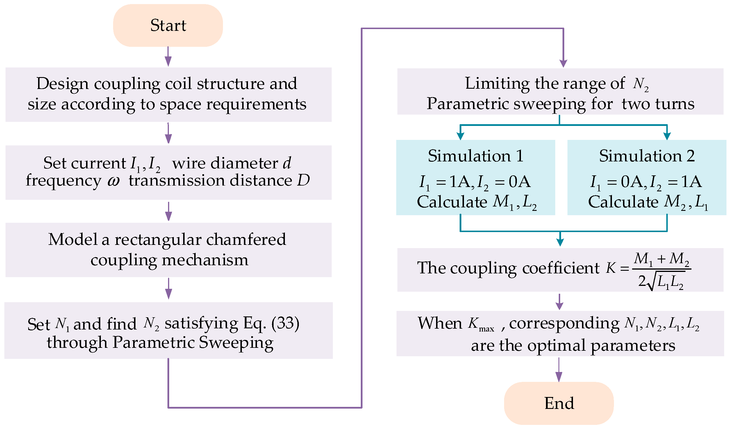
Firstly, the appropriate size and spacing of the two coils are designed according to the actual charging space requirements, the coupling coil model is built, and the magnetic field environment is set in COMSOL Multiphysics 6.0 finite element simulation software. Then, set a value of N 1 and perform a parametric sweep on N 2 so that its inductance value satisfies Equation (33). After limiting the range of N 2 , perform a parametric sweep on the turns of both coils. Two simulation experiments need to be performed to solve the self-inductance and mutual inductance, and the mean value of mutual inductance is taken for the calculation of coupling coefficient K . The number of primary turns corresponding to the maximum value of the coupling coefficient is selected as the optimal parameter of the system. The operation flow of COMSOL Multiphysics software is shown in Figure 4.
During the whole charging process, both primary and secondary coil currents should be less than the maximum current they can withstand, denoted by I ˙ 1 max and I ˙ 2 max . Their values need to be set in conjunction with the characteristics and parameters of the coils. In the following, the above condition is used as a constraint on the coil design for the self-inductance of the primary and secondary sides.
When the system is in the CC charging state, according to Equations (9) and (11), the following equation can be solved to obtain the current of the secondary coupling coil:
I ˙ 2 = ω 4 C S 1 2 M C P 1 R e q U ˙ a c B R i C
The system output current should also be less than the maximum current that the coil can withstand. According to Equation (24), the secondary coil current during charging needs to satisfy the following set of equations:
{ ω 4 C S 1 2 M C P 1 R e q U ˙ a c B R i C I ˙ 2 max ω 2 M C P 1 U ˙ a c E ( R 2 + R e q ) I ˙ 2 max
Neglecting R 2 and R i , the L 2 satisfies the following:
L 2 U o C S 1 R e q I ˙ 2 max
According to Equations (10) and (23), it can be seen that the primary coil current is unchanged before and after mode switching when R i is neglected, and combined with the full resonance condition, the current of the primary coil I ˙ 1 can be expressed as
I ˙ 1 = C P 1 U ˙ a c C P 2 ( L 1 L P 1 )
The primary side coil self-inductance L 1 needs to satisfy the following equation:
L 1 C P 1 2 U a c 2 + I 2 1 max C P 2 L P 1 I 2 1 max C P 2
Equations (36) and (38) serve as constraints to ensure the safety of the system’s primary side and secondary side circuits, and if the design does not satisfy the equations, the system parameters need to be redesigned.

3.2. Design of Compensation Components Parameter

To satisfy the varying voltage level demands of different loads, the compensation inductance L P 1 is determined according to the output voltage equation of the CV stage. According to Equation (28), the system output voltage gain G satisfies this equation:
G = U o U a c = M L P 1
If the required output voltage is greater than the input voltage, L P 1 < M can be set; conversely, if the required output voltage is lower than the input voltage, L P 1 > M can be set.
Since the primary compensation network realizes resonance, the series compensation capacitance C P 2 can be expressed as the following equation:
C P 2 = 1 ω 2 ( L 1 L P 1 )
As C P 2 is positive, the compensation inductance needs to satisfy L P 1 < L 1 . In summary, the constraints on the primary compensation inductance L P 1 are
{ M < L P 1 < L 1 , U a c > U o L P 1 < M , U a c < U o
With the primary side compensating inductance determined, the maximum input voltage on the DC side of the inverter circuit is solved based on Equations (28)–(30) as
U d c max = π 2 L P 1 U R L max 8 M
According to Equations (2), (4), and (18), when the system satisfies the full resonance condition, each compensation parameter can be expressed as
{ C P 1 = 1 ω 2 L P 1 C S 1 = 1 ω 2 L 2 L S 1 = 1 ω 2 C S 1
On the basis of the above analysis, the parameter design flow of the system is proposed, as shown in Figure 5.

4. Mode Switching Point Design

4.1. Analysis of the Load Switching Points

At the moment of lithium battery charging mode switching, the system output voltage may jump, i.e., the voltage rises or falls sharply in a short period of time. The reason for this is that the voltage of the same load is different in two different topologies. To minimize the effect of switching on the system voltage and power output stability, the voltage should be consistent before and after the switching point.
According to the CC mode output current Equation (15), combined with the equivalent resistance current and load current conversion relationship shown in Equation (31), the voltage of the load can be solved to meet the following equation in the CC mode:
U R L C C = I R L C C R L = 2 2 M U a c π ω L P 1 L S 1 R L
According to the CV mode output voltage Equation (28), combined with the equivalent resistance voltage and load voltage conversion relationship described in Equation (30), the voltage of load in the CV mode can be solved to satisfy the following equation:
U R L C V = 2 π M U a c 4 L P 1
When the equation U R L C C = U R L C V holds, the optimal switching resistance R b e s t , which ensures that the voltage does not jump at the switching point, satisfies the following equation:
R b e s t = π 2 ω L S 1 8
From the above equation, when the load target maximum voltage is 45 V, the optimal load switching point is R b e s t = 11.1   Ω corresponding to the equivalent resistance R e q = 9   Ω . The system parameters are detailed in Table 1.
In the following, the optimality of the load switching point obtained from Equation (46) is verified from the perspectives of the system output power and output efficiency.

4.2. Optimality Verification of the Switching Point

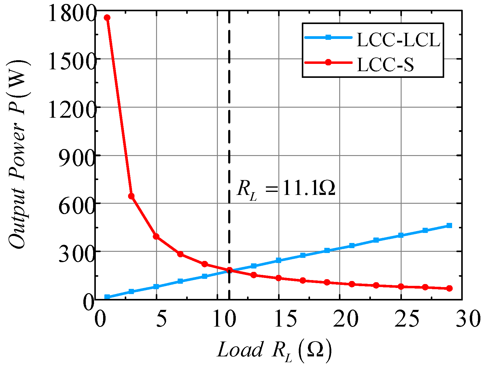
According to Equations (13) and (26), the curves of the variation of output power with the magnitude of load resistance for both topologies are presented in Figure 6.
From Figure 6, it is clear that the output power of two topologies changes with the load in the opposite trend, the power of the LCC-LCL type decreases progressively as the resistance value increases, with the rate of decrease eventually leveling off towards zero; while the power of the LCC-S type increases steadily with the load, maintaining an approximately constant rate of increase. At the optimal load switching point, two topologies’ output power is the same, which suggests that the fluctuations in the load voltage and current at the optimal load switching point are minimal, thereby ensuring the safety of both the system and the load.
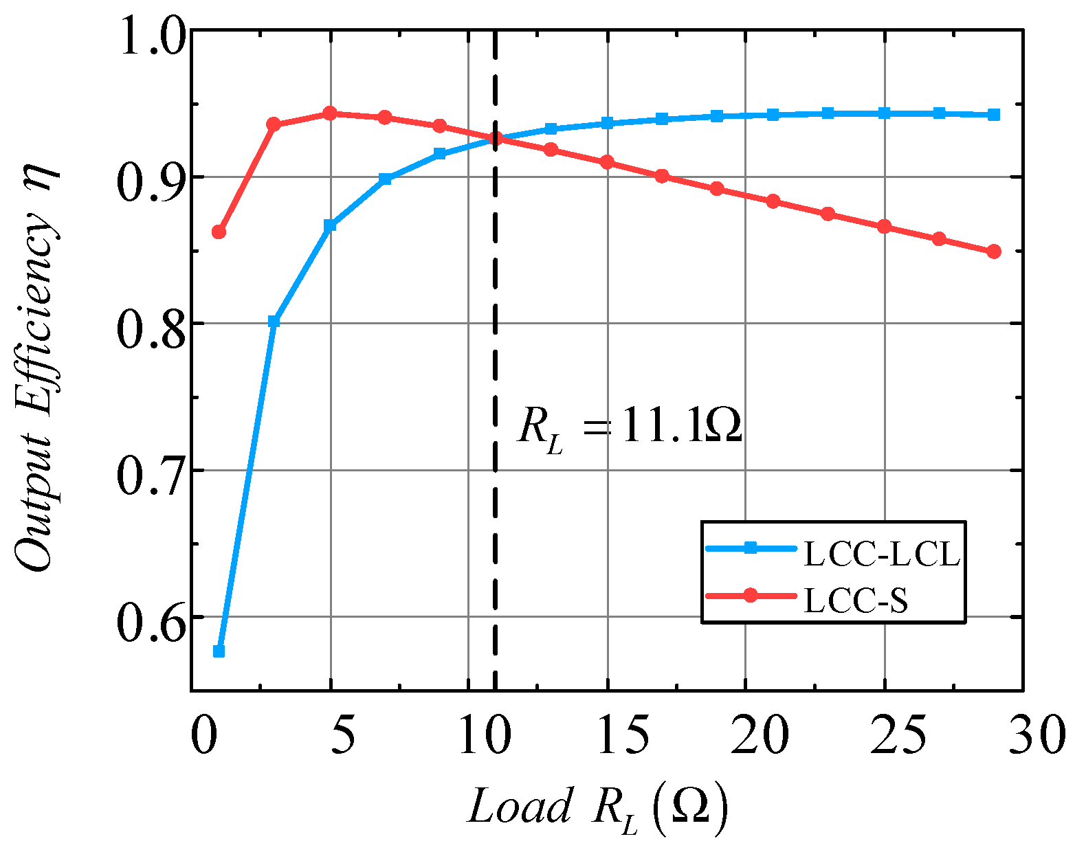
According to Equations (14) and (27), the curves of output efficiency with the load size for both topologies are plotted, as shown in Figure 7. At the optimal load switching point, the output efficiency of the two topologies is approximately equal and above 90%, indicating that the system maintains a high level of efficiency throughout the entire charge process, and the fluctuation of the power before and after the switching is small.
Based on the load switching point output power and efficiency analysis above, it can be seen that the topology switching of the system at this point minimizes the output fluctuation of the voltage and current. Further, to verify the optimality of the system output when the value of the load resistance is R b e s t , a simulation platform is built. The load resistance is set to be 5   Ω , 11.1   Ω , and 20   Ω , respectively. The simulation time is specified as 0.04 s and the topology switching at 0.02 s. The waveforms of load current and voltage before and after switching for different resistance conditions are shown in Figure 8.
Comparing and analyzing Figure 8, it is clear that when the load resistance value is the same as the optimal switching point resistance, the load voltage and current fluctuations are small and can reach a constant value in a short time, realizing the smooth switching of the output mode and verifying the optimality of the designed load switching point.

4.3. Design of Switching Control Strategy

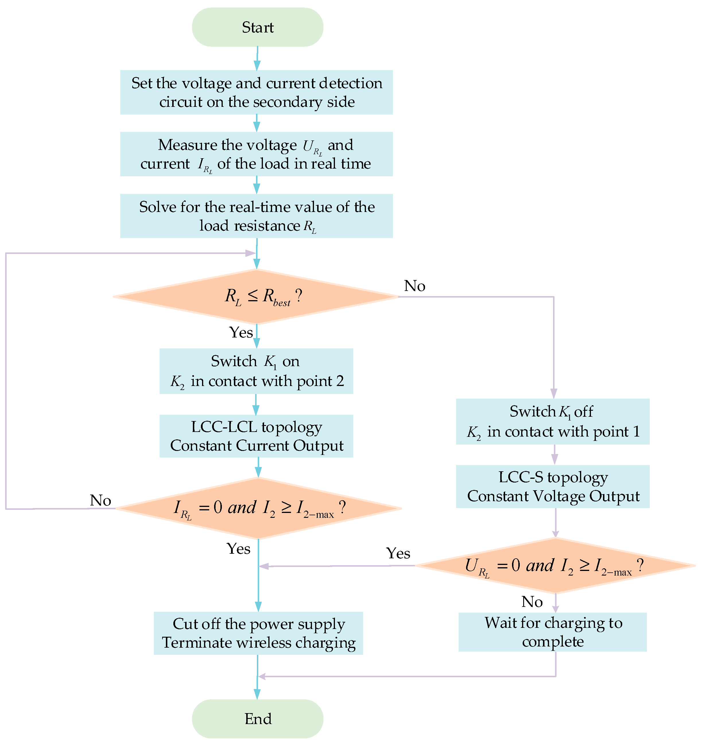
Based on the above analysis and verification of the optimal switching point, it can be seen that controlling the switching state at this point can achieve smooth switching of the output mode. The CC and CV mode switching control diagram is shown in Figure 9.
In this paper, voltage and current sampling circuits are set up on the secondary side to collect the voltage and current values of the load, respectively. The TMS320F28335 digital signal processor is used to process the collected data and to obtain the corresponding load resistance value. Lithium battery charging is a slow process; its sampling frequency requirements are not high, so the initial sampling frequency is set to once every 5 min. To accurately find the optimal switching resistance value, when the voltage reaches 90% of the preset voltage, the data acquisition and processing frequency are increased, and the sampling frequency is set to once every 1 min. Record N load resistance values to calculate the average value, when Equation (47) holds, the DSP will control the switch K 1 , K 2 switching to achieve the switching from CC to CV mode. If the formula is not satisfied, continue to repeat the above steps.
| i = 1 N R L i / N R b e s t R b e s t | 5 %
Moreover, during the actual running of the mentioned system, the special working condition of system no-load and load short-circuit may occur. To guarantee the security of WPT system operations, the following section analyzes the stability of the system under the two special working conditions and proposes the switching control strategy.

4.3.1. Analysis of System No-Load Condition

First, the influence of an open load on the WPT system during the CC output stage is analyzed, and its equivalent circuit is shown in Figure 10.
When the system is in resonance, the secondary impedance in CC mode satisfies Z C C 2 = R 2 . The impedance Z C C f from the secondary circuit equivalent to the primary side is
Z C C f = ( ω M ) 2 Z C C 2 = ( ω M ) 2 R 2
The primary input side input impedance is
Z C C I N = R 2 ( L 1 C P 2 ω 2 1 ) + R i C P 1 C P 2 ω 2 ( ω 2 M 2 + R 1 R 2 ) C P 1 C P 2 ω 2 ( ω 2 M 2 + R 1 R 2 )
For the constant current output and open load condition, the input current on the primary side is
I C C a c = U a c C P 1 C P 2 ω 2 ( ω 2 M 2 + R 1 R 2 ) R 2 ( L 1 C P 2 ω 2 1 ) + R i C P 1 C P 2 ω 2 ( ω 2 M 2 + R 1 R 2 )
The current of the two coils meet the following equations, respectively:
I ˙ C C 1 = j ω C P 1 U ˙ a c E
I ˙ C C 2 = ω 2 C P 1 U ˙ a c M E R 2
Since the parasitic internal resistance of the inductor is much smaller compared to its own impedance, it can be ignored. According to Equations (50)–(52), when the load is open-circuited, the current on the primary coil remains essentially unchanged, but the primary input current and the current on the secondary coil tend to infinity. To avoid system damage, it is necessary to terminate the power supply immediately.
Next, the influence of the load-open circuit on the system during the CV output stage is analyzed, and its equivalent circuit in this case is shown in Figure 11.
From the above figure, it can be seen that the system contains only the primary side circuit, which is equivalent to the fault case where the secondary side is missing. The secondary side impedance is infinity, and the impedance equivalent to the primary side from the secondary side is zero. The impedance of primary side input is calculated as
Z C V I N = Z C P 1 ( Z C P 2 + Z L 1 ) + R 1 R i R 1
The primary coil current is
I ˙ C V 1 = j ω C P 1 U ˙ a c E
Similarly, the inductive parasitic internal resistance is negligible. From Equation (53), the primary input impedance tends to infinity. When the load is open-circuit in the CV charging stage, the input circuit current is close to zero. From Equation (54), the primary coil current is only linked to the input voltage and switching the system frequency but is not affected by the change in the input current of the system. Therefore, when the load-open circuit condition occurs in the CV charging stage of the system, the possibility of system damage is very small.

4.3.2. Analysis of Load Short-Circuit Condition

When a short-circuit fault occurs on the secondary side of the system due to a burned rectifier bridge or thermal abuse of the battery, the safe operation of the system may be threatened. In the following, the magnitude of the primary and secondary side coils and the inverter output currents are analyzed when the load is short-circuited in CC and CV output modes, respectively. Figure 12 and Figure 13 show the equivalent circuit diagram of the system for a short-circuit fault in two modes.
From Figure 12, the equations R e q = 0   Ω and Z L S 1 + Z C S 1 = 0   Ω hold under resonant conditions, so the denominator of the impedance is equal to zero. The secondary impedance tends to infinity, so the current of the secondary coil is approximated to zero. The impedance from the secondary circuit equivalent to the primary side is zero. It is similar to the case of the system with no load in CV mode. From Figure 13, the equations R e q = 0   Ω and Z L 2 + Z C S 1 = 0   Ω hold, so the secondary equivalent impedance is equal to R 2 . It is similar to the case of the system with no load in CC mode.
Based on the above analysis, it can be seen that when the system is unloaded in CC mode or when the charging load is short-circuited in CV mode, both the secondary coil current and the inverter output current will increase substantially at the instant of switching, which may cause circuit faults, leading to system damage. When a disconnection or short-circuit fault occurs, if the secondary coil current is higher than the maximum current I 2 max can withstand, the coil temperature may rise in a short period of time, or even damage the circuit due to overheating. So, it is considered that the system is in an unstable operating state at this time, and it is necessary to terminate wireless charging immediately. A switch control strategy for short-circuit and open-load faults is shown in Figure 14.

5. System Simulation and Experiment Verification

To demonstrate the effectiveness of topology based on LCC-LCL/S and the parameter design method, a system simulation model is built using Simulink, a visual simulation tool in MATLAB R2021a. Two pulse generators are used to supply the MOSFETs with pulses at the frequency of 85 kHz, where the MOSFET S 1 and S 4 , S 2 and S 3 are in phase, and the phase difference between S 1 and S 2 is 180 degrees. The step signal is used to switch the ideal switching state in the simulation process, which can realize the switching of the topology or simulate the open-circuit and short-circuit conditions of the load. The system parameters are shown in Table 1.

5.1. Results Analysis of Simulation

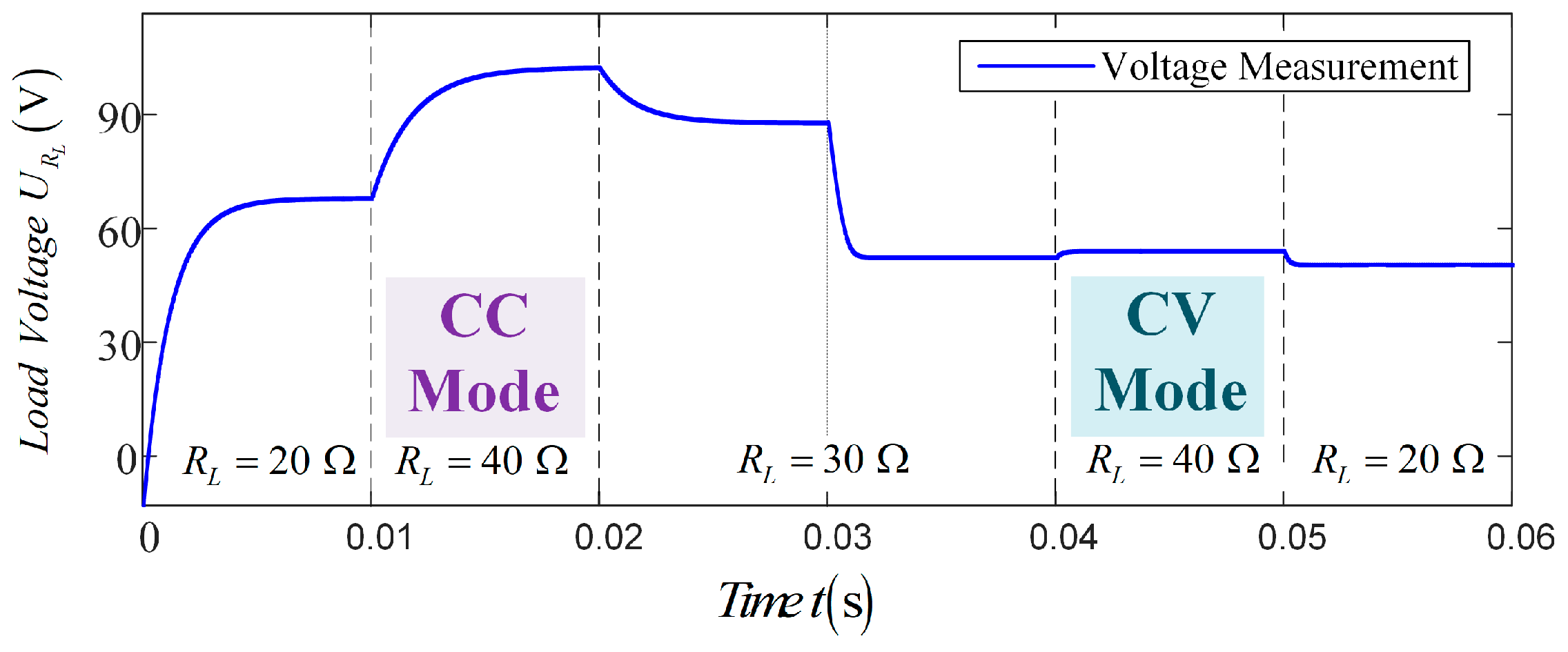
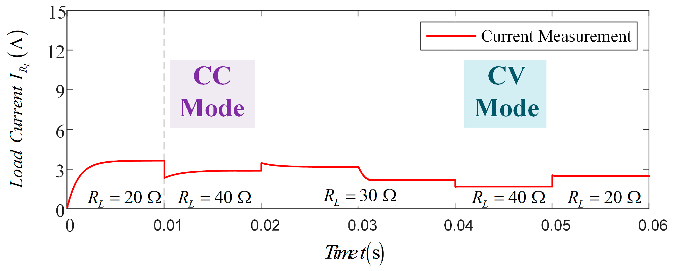
To verify the conclusion that this WPT system can switch the output mode from CC to CV when charging, the circuit model is built in Simulink for simulation experiments. Set the system working time as 0.06 s. The initial resistance value of the load is set as 20   Ω , and 0–0.03 s is the CC charging state. Switch the load every 0.01 s. The load resistance value is 20   Ω , 40   Ω , 30   Ω in turn. Switching topology at 0.03 s, the system enters the CV charging stage. Switch the load every 0.01 s. The load resistance is 30   Ω , 40   Ω , 20   Ω in turn. The variations of current and voltage at the inverter’s output under varying load conditions are shown in Figure 15 and Figure 16.
From Figure 15 and Figure 16, when the resistance of the load changes in the range of 20   Ω to 40   Ω , the current of the load remains essentially unchanged in the CC stage, with the maximum fluctuation within 0.2 A; in the CV stage, the load voltage remains essentially unchanged, with the maximum fluctuation within 2.5 V. Therefore, it can be demonstrated that topology can achieve CC and CV output.
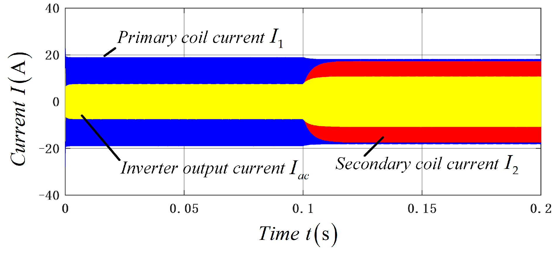
Next, the primary coil current, secondary coil current, and system output current are simulated when the load is disconnected in the CC mode. The simulation time is specified as 0.2 s, and the load is disconnected at 0.1 s. The waveform of the current change before and after the load disconnection in the CC stage is presented in Figure 17.
Figure 17 shows the current waveform with the load disconnected in the CC charging mode. Among them, the transmitter coil current remains essentially unchanged before and after the load is opened, while the full-bridge inverter circuit output current and receiver coil current show an obvious increasing trend at 0.1 s, which confirms the validity of the theoretical derivation in Section 4.3.

5.2. Results Analysis of the Experiment

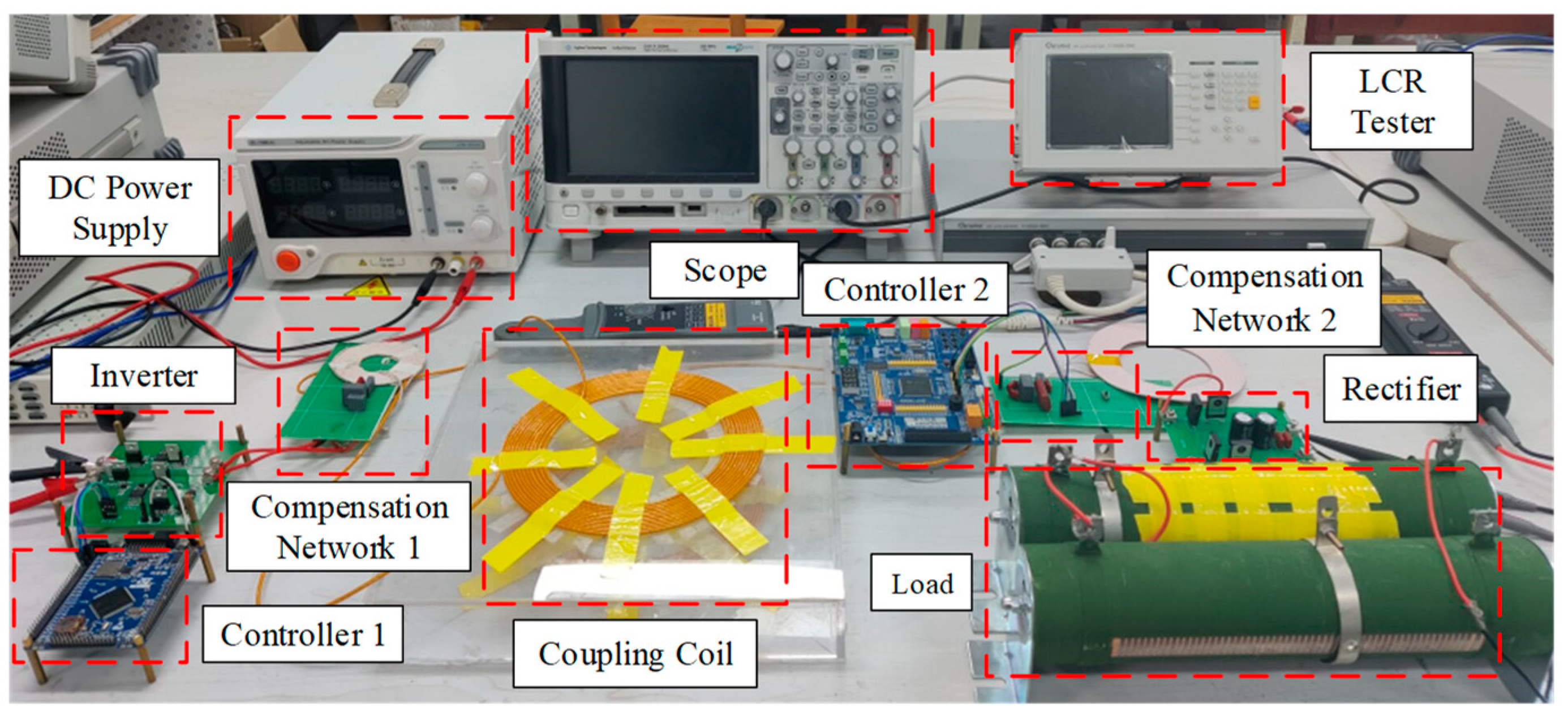
To prove the feasibility of the charging system for charging batteries in real situations, an experimental platform was built based on the system circuit presented in Figure 1, which is shown in Figure 18. The experiment parameters are shown in Table 1.
The system input side adopts a high-power adjustable DC-regulated power supply; the system selects an STM32F407 microcontroller as the main controller of the primary side to realize the control of the inverter circuit; it adopts a high-frequency full-bridge inverter circuit composed of 60R060P7 low-resistance field-effect transistors; it selects the IR2110S with a small volume and a high degree of integration as the driver chip of the inverter circuit; the secondary main controller is a TMS320F28335 DSP processor; it is used to collect and process the data of the load voltage and current in real-time; an E5PH6012L fast recovery diode is used to form the rectifier circuit; a Chroma 11050-5M is used to measure two coils’ self-inductance and mutual inductance; the Tektronix MSO 2024B oscilloscope was used to record the experimental waveforms.
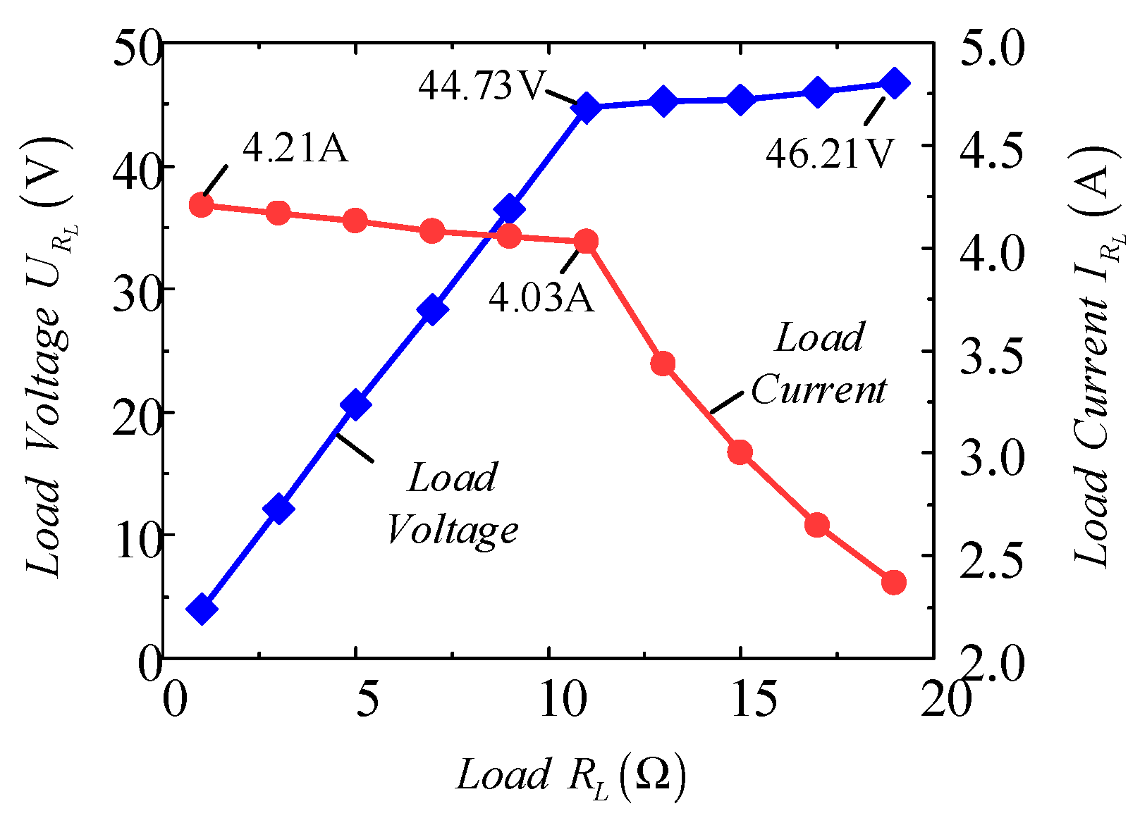
To investigate whether the system can achieve constant output under real charging conditions, the load current and voltage values were recorded during the period when load resistance increased from 1   Ω to 20   Ω . The voltage and current curves of the load during charging are shown in Figure 19.
From Figure 19, throughout the charging process, when the load grows from 1   Ω to 11.1   Ω , the load voltage gradually rises, and the load current remains essentially unchanged, with the current fluctuating within 0.2 A. After switching topology, as the resistance of the load increases, the voltage of the load remains essentially unchanged and the current of the load gradually decreases, with the voltage fluctuating within 3 V. The system achieves a maximum output voltage of 46.21 V and a maximum output power of 180 W.
To verify that the system satisfies ZPA characteristics, the inverter output voltage and current are analyzed for the single topology under different resistance conditions, respectively. Figure 20 and Figure 21 show the output voltage and current waveforms of the inverter when the secondary side is LCL-type and S-type topology, respectively.
From Figure 20 and Figure 21, it is clear that the current and voltage remain in the same phase with different values of load resistance, which satisfies the ZPA characteristic.
Figure 22 shows the waveforms of the load voltage and current before and after switching. Analyzing the waveforms, it is clear that when the load resistance meets the equation R L = 11.1   Ω , the load voltage increases, and the voltage fluctuation is within 0.2 V; the current of the load increases slightly, and the current fluctuation is within 0.02 A. After the switching is completed, the voltage and current of the load are restored to constant, and the magnitude of the values is basically the same as before switching, realizing the stable switching of the charging mode.
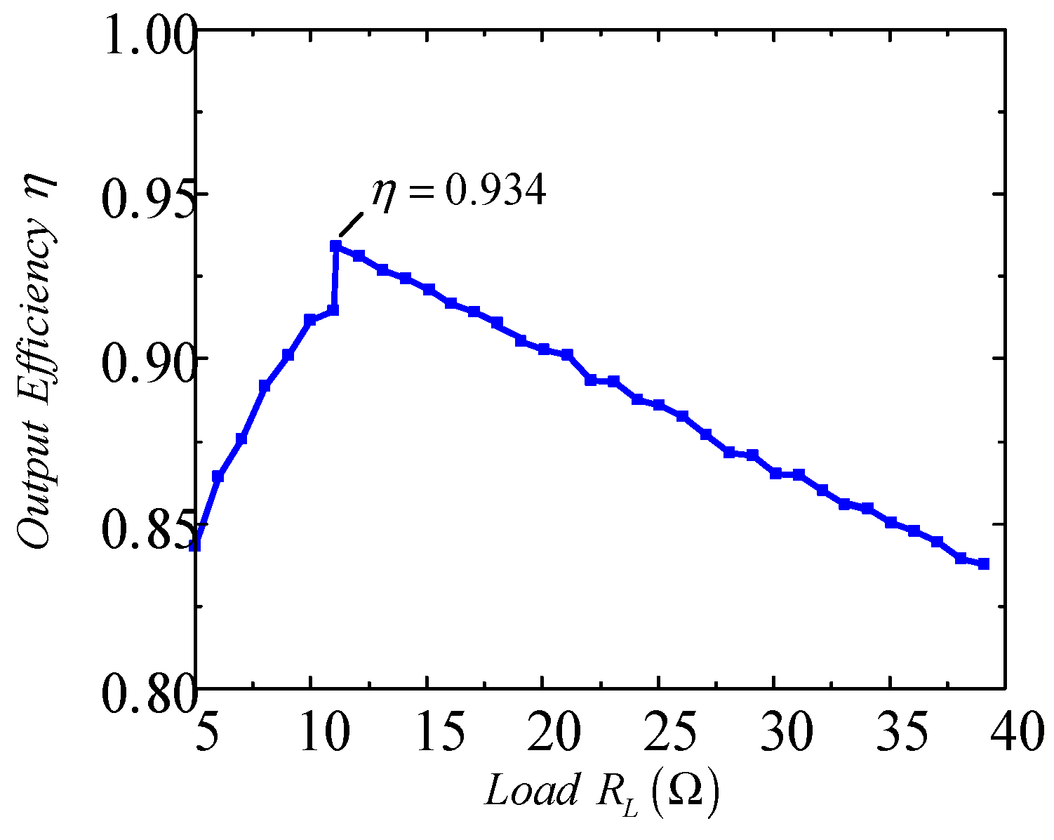
To verify the conclusion that the system output efficiency at the optimal load switching point before and after switching remains basically unchanged and in a high-efficiency state, the system output efficiency is analyzed when R L increases from 5   Ω to 40   Ω during the charging process. Figure 23 shows the variation of the system output efficiency in the whole charging process.
From Figure 23, it is clear that the system output efficiency in the CC output state improves as the resistance is increased, reaching a maximum of 91.6%. In contrast, the efficiency in the CV output state falls as the resistance increases, with a peak efficiency of 93.4%. The efficiency fluctuation at the switching point is 1.8%, and the system whole output efficiency is above 83.5%, which verifies the validity of the theoretical derivation in Section 4.2.
To further illustrate the superiority of the mentioned topology and methodology, the conclusions of this study compared to earlier studies are shown in Table 2.
By comparison, the advantages of the system in this study are listed below:
  • Compared with Refs. [29,34,37], this system uses two coils to achieve wireless energy transmission, with fewer coils and a smaller overall system size, which is more suitable for space-constrained application scenarios.
  • Compared with Refs. [35,36], a novel hybrid topology is designed to realize the constant output and switch charging state of the system, using fewer compensation components and two switches, and the proposed system parameters design methodology is used to achieve the efficient output of the system under ZPA conditions.

6. Conclusions

To ensure the stability and high efficiency of wireless charging for batteries, this paper proposes a novel hybrid compensation topology based on LCC-LCL/S. Smooth switching of the CC and CV charging states is achieved by controlling the switches to change the secondary side compensation network, which significantly reduces the control complexity. Considering the maximum safe current constraints of the system, the parameter design method under resonance conditions is proposed to effectively avoid potential safety risks. The system is analyzed from the perspective of the mode switching point and special working conditions like no-load and short-circuit, and the switching control strategy is given. The results from the simulation and experiment indicate that the proposed parameter design method and the optimal load point design are feasible; the battery voltage fluctuation at the mode switching point can be realized within 0.2 V, and the current fluctuation within 0.02 A, which ensures the safe and stable running of the WPT system. Throughout the whole charging process, the system achieves high output efficiency, and the maximum output efficiency can reach 93.4%, which has good prospects for practical engineering applications.

Author Contributions

Conceptualization, T.S. and W.H.; methodology, T.S.; software, T.S. and T.R.; validation, T.R. and Y.C.; formal analysis, T.S.; investigation, W.H. and Y.C.; resources, W.H. and H.Y.; data curation, T.R.; writing—original draft preparation, T.S. and W.H.; writing—review and editing, T.S., W.H. and H.Y.; visualization, Y.C. and T.R.; supervision, W.H., Y.C. and H.Y. All authors have read and agreed to the published version of the manuscript.

Funding

This research was funded by the National Natural Science Foundation of China (grant number: 61903129) and the “High-level” Talents Funding Program of Hubei University of Technology (grant number: BSQD2020012).

Data Availability Statement

Data are contained within the article.

Conflicts of Interest

The authors declare no conflicts of interest.

Abbreviations

LCC-LCL/SThe reconfigurable topology is composed of LCC-LCL and LCC-S.
WPTWireless power transfer
CCConstant current
CVConstant voltage
ZPAZero phase angle

References

  1. Vinod, M.; Kishan, D.; Kannan, R.; Iqbal, A.; Mohammed Sulthan, S. Primary side control strategies for battery charging regulation in wireless power transfer systems for EV applications. IET Power Electron. 2024, 1–12. [Google Scholar] [CrossRef]
  2. Liu, S.G.; Ye, Z.X.; Lu, W.B. Electric vehicle dynamic wireless charging technology based on multi-parallel primary coils. IEEE Int. Conf. Electron. Commun. Eng (ICECE) 2018, 12, 120–124. [Google Scholar]
  3. Liu, X.; Gao, F.; Niu, H.; Sun, G.; Wang, T.; Wang, H. A Series–Parallel Transformer-Based WPT System for 400-V and 800-V Electric Vehicles with Z1 or Z2 Class. IEEE Trans. Power Electron. 2024, 39, 1749–1761. [Google Scholar] [CrossRef]
  4. Yang, B.; Zhang, Y.; Zhu, C.; Sahoo, S.; Chen, Y.; Mai, R.; He, Z.; Blaabjerg, F. A Design Method to Minimize Detuning for Double-Sided LCC-Compensated IPT System Improving Efficiency Versus Air Gap Variation. IEEE Trans. Power Electron. 2024, 39, 1723–1737. [Google Scholar] [CrossRef]
  5. Gnanavendan, S.; Selvaraj, S.K.; Dev, S.J.; Mahato, K.K.; Swathish, R.S.; Sundaramali, G.; Accouche, O.; Azab, M. Challenges, Solutions and Future Trends in EV-Technology: A Review. IEEE Access 2024, 12, 17242–17260. [Google Scholar] [CrossRef]
  6. Pang, S.; Xu, J.Y.; Li, H.Y.; Ma, Q.; Li, X. Dual-Frequency Modulation to Achieve Power Independent Regulation for Dual-Load Underwater Wireless Power Connector. IEEE J. Emerg. Sel. Top. Power Electron. 2023, 11, 2377–2389. [Google Scholar] [CrossRef]
  7. Mostafa, A.; Wang, Y.; Tangirala, S.; Zhang, H.; Lu, F. A 5 kW Hull-Compatible Inductive Charging System with 360° Folded Spatial Unipolar Coupler for Autonomous Underwater Vehicles (AUVs). IEEE Trans. Ind. Appl. 2023, 59, 7001–7012. [Google Scholar] [CrossRef]
  8. Shah, I.A.; Zada, M.; Shah, S.A.A.; Basir, A.; Yoo, H. Flexible Metasurface-Coupled Efficient Wireless Power Transfer System for Implantable Devices. IEEE Trans. Microw. Theory Tech. 2024, 72, 2534–2547. [Google Scholar] [CrossRef]
  9. Xue, Z.; Chau, K.T.; Liu, W.; Hua, Z. Magnetic-Free Wireless Self-Direct Drive Motor System for Biomedical Applications with High-Robustness. IEEE Trans. Power Electron. 2024, 39, 2882–2891. [Google Scholar]
  10. Pahlavan, S.; Ashtiani, S.J. Rotation-Tolerant Wireless Power Transmission Scheme with Smart Positioning for Cognitive Research on Moving Animals. IEEE Trans. Biomed. Circuits Syst. 2024, 18, 123–130. [Google Scholar] [CrossRef]
  11. Yang, Y.; Cao, G.; Li, H. A Positioning and Direction-Guided Approach of the WPT System Based on the Triple-U Coil. IEEE Sens. J. 2023, 23, 26473–26485. [Google Scholar] [CrossRef]
  12. Khan, S.R.; Desmulliez, M.P.Y. Investigation of Capsule Localization using 3-D Printed Spiral WPT Coil. In Proceedings of the 2023 17th European Conference on Antennas and Propagation (EuCAP), Florence, Italy, 26–31 March 2023; pp. 1–5. [Google Scholar]
  13. Zhou, J.L.; Zhang, B.; Xiao, W.X.; Qiu, D.Y.; Chen, Y.F. Nonlinear parity-time-symmetric model for constant efficiency wireless power transfer: Application to a drone-in-flight wireless charging platform. IEEE Trans. Ind. Electron. 2019, 66, 4097–4107. [Google Scholar] [CrossRef]
  14. Hannan, M.A.; Hoque, M.D.M.; Hussain, A.; Yusof, Y.; Ker, A.P.J. State-of-the-art and energy management system of lithium-ion batteries in electric vehicle applications: Issues and recommendations. IEEE Access 2018, 6, 19362–19378. [Google Scholar] [CrossRef]
  15. Wang, D.Y.; Fu, C.W.; Zhao, Q.L.; Hu, T. A PSO-based optimization design of W-type non contact transformer for stable power transfer in DWPT system. IEEE Trans. Ind. Appl. 2022, 58, 1211–1221. [Google Scholar] [CrossRef]
  16. Sun, Z.; Chi, Y.; Wang, Y.; Guan, Y.; Xu, D. Analysis and Design of a High Frequency Wireless Battery Charging System with Smooth Mode Transition Characteristics. IEEE Trans. Power Electron. 2023, 38, 13273–13285. [Google Scholar] [CrossRef]
  17. Mai, R.K.; Chen, Y.; Li, Y.; Zhang, Y.Y.; Cao, G.Z.; He, Z.Y. Inductive Power Transfer for Massive Electric Bicycles Charging Based on Hybrid Topology Switching with a Single Inverter. IEEE Trans. Power Electron. 2017, 32, 5897–5906. [Google Scholar] [CrossRef]
  18. Chen, Y.; Zhang, H.; Park, S.-J.; Kim, D.-H. A Comparative Study of S-S and LCCL-S Compensation Topologies in Inductive Power Transfer Systems for Electric Vehicles. Energies 2019, 12, 1913. [Google Scholar] [CrossRef]
  19. Yeo, T.-D.; Kwon, D.; Khang, S.-T.; Yu, J.-W. Design of Maximum Efficiency Tracking Control Scheme for Closed-Loop Wireless Power Charging System Employing Series Resonant Tank. IEEE Trans. Power Electron. 2017, 32, 471–478. [Google Scholar] [CrossRef]
  20. Wu, L.H.; Zhang, B.; Jiang, Y.W. Position-Independent Constant Current or Constant Voltage Wireless Electric Vehicles Charging System without Dual-Side Communication and DC–DC Converter. IEEE Trans. Ind. Electron. 2022, 69, 7930–7939. [Google Scholar] [CrossRef]
  21. Mo, Y.H.; Wang, Y.; Xiao, J.; Chen, S.N.; Wu, N.; Wu, X.R. Analysis of MC-WPT Analysis in LCC-S Resonant Network Based on Frequency Switching Control. In Proceedings of the 2023 IEEE 5th International Conference on Civil Aviation Safety and Information Technology (ICCASIT), Dali, China, 11–13 October 2023; pp. 235–239. [Google Scholar]
  22. Yang, L.; Geng, Z.; Jiang, S.; Wang, C. Analysis and Design of an S/PS−Compensated WPT System with Constant Current and Constant Voltage Charging. Electronics 2022, 11, 1488. [Google Scholar] [CrossRef]
  23. Voottipruex, K.; Mujjalinvimut, E.; Sangswang, A.; Naetiladdanon, S. A Load-Independent Operation of WPT under Frequency Bifurcation for Battery Charging Applications. In Proceedings of the IECON 2020 the 46th Annual Conference of the IEEE Industrial Electronics Society, Singapore, 18–21 October 2020; pp. 2573–2578. [Google Scholar]
  24. Yang, L.; Ren, L.; Shi, Y.Y.; Wang, M.; Geng, Z. Analysis and Design of an S/S/P-Compensated Three-Coil Structure WPT System with Constant Current and Constant Voltage Output. IEEE J. Emerg. Sel. Top. Power Electron. 2023, 11, 2487–2500. [Google Scholar] [CrossRef]
  25. Kim, M.; Joo, D.-M.; Lee, B.K. Design and control of inductive power transfer system for electric vehicles considering wide variation of output voltage and coupling coefficient. IEEE Trans. Power Electron. 2019, 34, 1197–1208. [Google Scholar] [CrossRef]
  26. Cheng, B.; He, L. High-Order Network Based General Modeling Method for Improved Transfer Performance of the WPT System. IEEE Trans. Power Electron. 2021, 36, 12375–12388. [Google Scholar] [CrossRef]
  27. Li, K.; Gong, Z.; Liu, Q.; Zheng, S.Y.; Liu, J.Y.; Wang, S.Z. A MCR-WPT system based on LCL-S/P hybrid compensation network with CC/CV and maximum power optimization suiting for battery charging. IET Power Electron. 2024, 17, 351–363. [Google Scholar] [CrossRef]
  28. Qu, X.; Han, H.; Wong, S.; Tse, C.K.; Chen, W. Hybrid IPT topologies with constant current or constant voltage output for battery charging applications. IEEE Trans. Power Electron. 2015, 30, 6329–6337. [Google Scholar] [CrossRef]
  29. Chen, Y.; Yang, B.; Kou, Z.H.; He, Z.Y.; Cao, G.Z.; Mai, R.K. Hybrid and Reconfigurable IPT Systems with High-Misalignment Tolerance for Constant-Current and Constant-Voltage Battery Charging. IEEE Trans. Power Electron. 2018, 33, 8259–8269. [Google Scholar] [CrossRef]
  30. Li, Y.; Hu, J.; Liu, M.; Chen, Y.; Chan, K.W.; He, Z.; Mai, R. Reconfigurable Intermediate Resonant Circuit Based WPT System with Load-Independent Constant Output Current and Voltage for Charging Battery. IEEE Trans. Power Electron. 2019, 34, 1988–1992. [Google Scholar] [CrossRef]
  31. Shen, Z.W.; Zhou, H.Y.; Tang, H.M.; Zhuang, Y.H.; Mao, X.K.; Zhang, Y.M. A Misalignment-Insensitive Wireless Charging System with Constant-Voltage and Constant-Current Charging Capabilities. In Proceedings of the 2023 10th International Conference on Power and Energy Systems Engineering (CPESE), Nagoya, Japan, 8–10 September 2023; 43–48. [Google Scholar]
  32. Cheng, B.; He, L.; Liu, H. Optimization Method for High-Order Wireless Power Transfer System Considering Gain Constraint and Components Stress. IEEE Trans. Transp. Electrif. 2023. [Google Scholar] [CrossRef]
  33. Gyimothy, S.; Kaya, S.; Obara, D.; Shimada, M.; Masuda, M.; Bilicz, S.; Pavo, J.; Varga, G. Loss Computation Method for Litz Cables with Emphasis on Bundle-Level Skin Effect. IEEE Trans. Magn. 2019, 55, 1–4. [Google Scholar] [CrossRef]
  34. Zhang, Y.; Wei, G.; Wang, C.; Yin, Y.; Feng, J.; Na, T.; Song, K.; Zhu, C. A Hybrid Compensation Topology with Constant Current and Constant Voltage Outputs for Wireless Charging System. IEEE Trans. Transp. Electrif. 2023, 9, 2070–2080. [Google Scholar] [CrossRef]
  35. Hwang, S.-H.; Chen, Y.; Zhang, H.; Lee, K.-Y.; Kim, D.-H. Reconfigurable Hybrid Resonant Topology for Constant Current/Voltage Wireless Power Transfer of Electric Vehicles. Electronics 2020, 9, 1323. [Google Scholar] [CrossRef]
  36. Guo, X.; Qi, Y.-S.; Liu, L.-Q.; Jia, S.-Y.; Mi, L.-J. Resonant wireless charging scheme. Energy Rep. 2023, 9 (Suppl. S3), 612–621. [Google Scholar] [CrossRef]
  37. Li, Y.; Hu, J.F.; Chen, F.B.; Liu, S.P.; Yan, Z.T.; He, Z.Y. A New-Variable-Coil-Structure-Based IPT System with Load-Independent Constant Output Current or Voltage for Charging Electric Bicycles. IEEE Trans. Power Electron. 2018, 33, 8226–8230. [Google Scholar] [CrossRef]
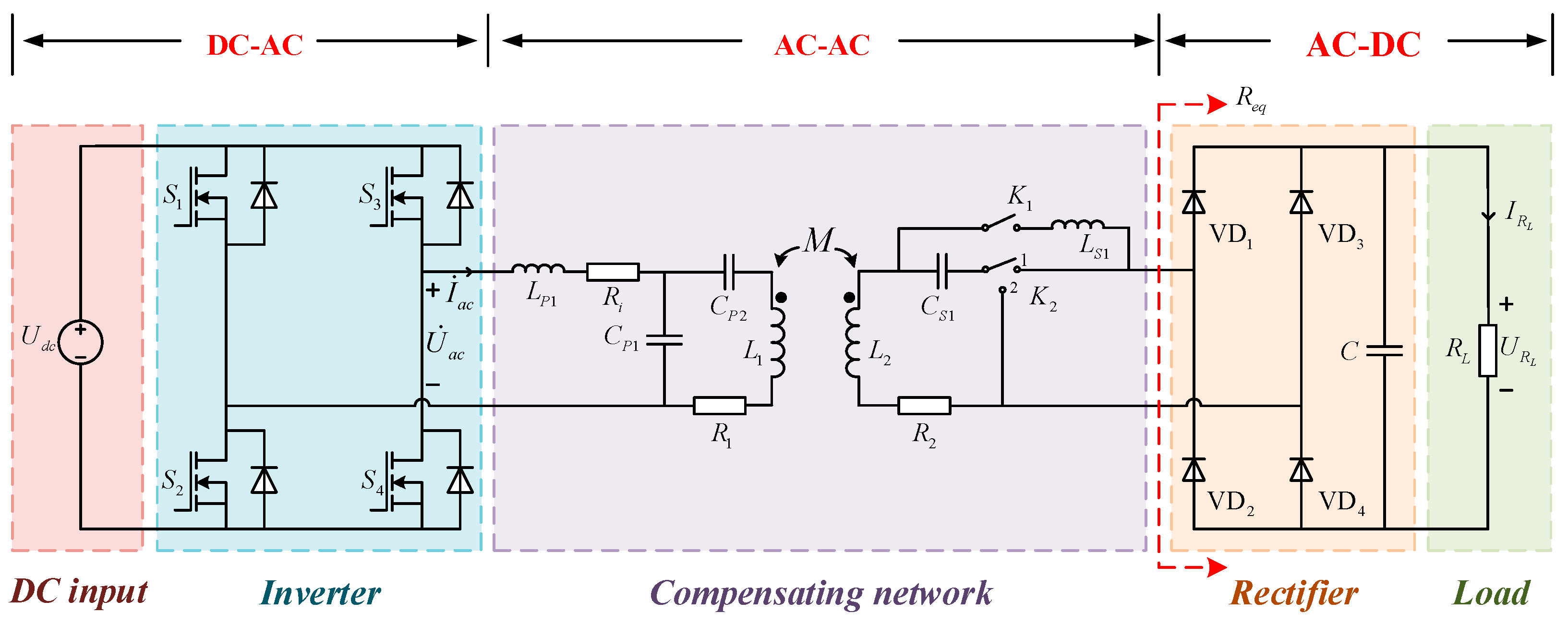
Figure 1. LCC-LCL/S-type CC and CV self-switching circuit.
Electronics 13 01729 g001
Figure 2. The LCC-LCL equivalent mutual inductance circuit.
Electronics 13 01729 g002
Figure 3. The LCC-S equivalent mutual inductance circuit.
Electronics 13 01729 g003
Figure 4. The operation flow of COMSOL Multiphysics software.
Electronics 13 01729 g004
Figure 5. The system parameters design flowchart.
Electronics 13 01729 g005
Figure 6. The system output power curve.
Electronics 13 01729 g006
Figure 7. System output efficiency curve.
Electronics 13 01729 g007
Figure 8. The waveforms of load current and voltage before and after switching for different resistance values.
Electronics 13 01729 g008
Figure 9. The CC and CV mode switching control diagram.
Electronics 13 01729 g009
Figure 10. The load-open equivalent circuit in the constant current mode.
Electronics 13 01729 g010
Figure 11. The load-open equivalent circuit in the constant voltage mode.
Electronics 13 01729 g011
Figure 12. The equivalent circuit of the system for a short-circuit fault in CC mode.
Electronics 13 01729 g012
Figure 13. The equivalent circuit of the system for a short-circuit fault in CV mode.
Electronics 13 01729 g013
Figure 14. Switch control strategy for short-circuit and open-load faults.
Electronics 13 01729 g014
Figure 15. Output voltage waveforms of inverters with variable loads.
Electronics 13 01729 g015
Figure 16. Output current waveforms of inverters with variable loads.
Electronics 13 01729 g016
Figure 17. Waveforms of current before and after load disconnection in the CC state.
Electronics 13 01729 g017
Figure 18. The experiment platform.
Electronics 13 01729 g018
Figure 19. The load voltage and current variation curves during charging.
Electronics 13 01729 g019
Figure 20. The LCC-LCL topology output waveforms of inverter with different load.
Electronics 13 01729 g020
Figure 21. The LCC-S topology output waveforms of inverter with different load.
Electronics 13 01729 g021
Figure 22. Load voltage and current waveforms before and after switching.
Electronics 13 01729 g022
Figure 23. The system output efficiency curve of the whole charging process.
Electronics 13 01729 g023
Table 1. System parameters.
SymbolVariableValue
U d c DC input 100   V
f Operating frequency 85   kHz
L 1 Coil-1 self-inductance 18 . 9   μ H
L 2 Coil-2 self-inductance 16.8   μ H
L P 1 Primary side inductance 11.9   μ H
C P 1 Primary side parallel capacitance 294.2   nF
C P 2 Primary side series capacitance 498.1   nF
C S 1 Secondary side capacitance 208.1   nF
L S 1 Secondary side inductance 16.8   μ H
C Filter capacitance 300   μ F
M Mutual inductance 5.36   μ H
Table 2. Comparison of this scheme with similar schemes that have been proposed.
Ref. [29]Ref. [34]Ref. [35]Ref. [36]Ref. [37]Proposed
TopologyFour-coilThree-coilS/LCC-SLCL-LCL/SFour-coilLCC-LCL/S
Coils432242
Switches212222
Location of switchesSecondary sidePrimary sidePrimary sideSecondary sidePrimary sideSecondary side
Primary side compensation components424232
Secondary side compensation components811212
Efficiency93.9%94.4%92.58%84%91.014%93.4%
Disclaimer/Publisher’s Note: The statements, opinions and data contained in all publications are solely those of the individual author(s) and contributor(s) and not of MDPI and/or the editor(s). MDPI and/or the editor(s) disclaim responsibility for any injury to people or property resulting from any ideas, methods, instructions or products referred to in the content.