Article

Research on Low-Insertion-Loss Packaging Materials for DC-6 GHz Attenuation Chips

by
Zhijie Wei
1,*,
Shenglin Yu
1 and
Pengcheng Wei
2
1
College of Electronic and Information Engineering, Nanjing University of Information Science and Technology, Nanjing 210044, China
2
Chinese People’s Liberation Army Army Chemical Defense College, Beijing 102205, China
*
Author to whom correspondence should be addressed.
Electronics 2024, 13(9), 1785; https://doi.org/10.3390/electronics13091785
Submission received: 10 March 2024 / Revised: 24 April 2024 / Accepted: 30 April 2024 / Published: 6 May 2024

Abstract

:
In the DC-6 GHz band, low-insertion-loss packaging materials were investigated to effectively reduce the heat generated during the working process of the attenuation chip. Based on the working principle of the attenuation chip, when the signal passes through the attenuation chip resistor network, it results in energy loss. This means that the insertion loss of the chip generates heat, which leads to an uneven heat dissipation of the chip and thus functional failure. The microwave characteristics of the packaged joints were investigated using different packaging techniques. The results show that the S21 and S11 of the attenuation chip after nano-silver and Au80Sn20 packaging are optimal in the frequency band of DC-6 GHz, and the insertion loss is low compared with the commonly used packaging materials Sn60Pb40 and Sn96.5Ag3.5, which reduces the heat loss and improves the reliability of the attenuation chip packaging.

1. Introduction

Chip packaging is a core part of semiconductor technology, which has a wide range of applications in aerospace, electric vehicles, industrial control and other fields [1]. With the increases in chip package density and the reductions in chip size, the problem of chip heat dissipation has become a hot research issue, so the packaging technology connecting the chip and the carrier board is also facing great challenges [2]. In the encapsulation process, the role of the encapsulation material is to connect the chip and the carrier board closely together to form a reliable electrical connection. In order to meet the performance requirements, the packaging material must have excellent electrical conductivity, heat resistance and reliability [3,4]. In addition, the loss generated during the chip’s operation is caused by the resistivity and thermal conductivity of the packaging material, resulting in an increase in the chip temperature, thus affecting the power output and reliability [5].
In recent years, scholars domestically and internationally have also conducted a lot of research on the impact of packaging materials on chip packaging. Zhou B. et al. [6] addressed the use of Sn60Pb40 solder for PBGA soldering experiments, through the real-time detection of the failure mechanism of solder joints under the load of temperature cycling, as a way to predict the fatigue coefficient and life of the solder layer. To lay the foundation for reliability research. Xiang Luoyi et al. [7] selected Sn99.3Cu0.7, Sn96.5Ag3.5 and Sn95Sb5, which are three kinds of welding materials, for welding experiments, through a comparison of the void rates of Sn99.3Cu0.7 solder and Sn96.5Ag3.5 solder, the void rate was lower than that of Sn95Sb5 solder for the selection of the welding layer material to provide a certain theoretical support. Depiver Joshua A et al. [8] Sn63Pb37 and SnAgCu(SAC)305, 387, 396 and 405 solders were used for the characterization simulation of the random vibration response of BGA solder joints, and the results showed that the deformation of Sn63Pb37 solder was the smallest, while the equivalent force was the largest, the fatigue life of SAC405 solder was the highest, and the fatigue life of SAC387 solder was the lowest. Lee Jing Rou et al. [9] used three kinds of solder, SAC305, SAC405 and SnBi, to analyze the deformation and stress of BGA solder joints, and they found that the deformation and stress in the reflow soldering of SAC305 solder were much better than those of SAC405 and SnBi solder. Michael Thomas Craton et al. [10] focused on active, passive devices integrated on a carrier board that were packaged in such a way that the microwave performance did not degrade after stressing the part through power cycling and temperature cycling (temperature gradient of 10 °C/min to 200 °C).
Previous studies have focused on exploring the reliability of packaged chips with different packaging materials in terms of soldering, temperature cycling and mechanical vibration. In this paper, the effects of different packaging materials on the microwave performances of attenuation chips in the DC-6 GHz band are presented, and experiments were conducted to investigate the effects of four packaging materials, including Sn60Pb40, Au80Sn20, Sn96.5Ag3.5 and nano-silver, on the reliability of the encapsulation of attenuation chips. Firstly, the interconnection of the chip with the carrier board was carried out according to the vacuum eutectic welding process and nano-silver sintering process for different packaging materials to provide samples for the study on the microwave performances of power chips. Second, a microwave parameter test board was designed to interconnect the microstrip line and the encapsulated completed attenuation chip by bonding alloy wire. Finally, the effects of different packaging materials on the insertion loss (S21) and return loss (S11) of the attenuation chip were investigated using the unpackaged attenuation die as a control group.

2. Methods

2.1. Experimental Model

The package connector structure consists of three parts: a chip layer, connection layer and carrier board layer. The chip layer is a fixed GaAs attenuator chip with 5 dB attenuation in the DC-6 GHz band, with a size of 0.5 × 0.7 × 0.02 mm3, a protective layer on the front and a gold-plated ground on the back, which is used through the package and gold wire connection. In order to maintain the symmetry of the attenuation network, the design process has the two resistors in series be equal in resistance (R1 = R3 = 14.006 ohm and R2 = 82.214 ohm) [11]. The thickness of the connecting layer was 0.025 mm, and the area was matched to the chip. The substrate was a copper substrate of Mo85Cu15 with a size of 1 × 1 × 0.05 mm3. A model diagram is shown in Figure 1 below.
Microwave circuits are usually high-frequency, so the grounding condition of the chip affects the circuit crosstalk and insertion loss, as well as brings additional capacitance and oscillation. The GaAs substrate material of the high-power microwave chip in the transmitting part of the microwave assembly has poor thermal conductivity, so the connection between the high-power microwave chip and the substrate must have a good microwave grounding capability (low ohmic contact) and resistivity. Therefore, the physical parameters of the experimental model have an important role in the packaging of the chip, and the physical parameters of each layer in the model [12,13,14] are shown in Table 1 below.

2.2. Experimental Model

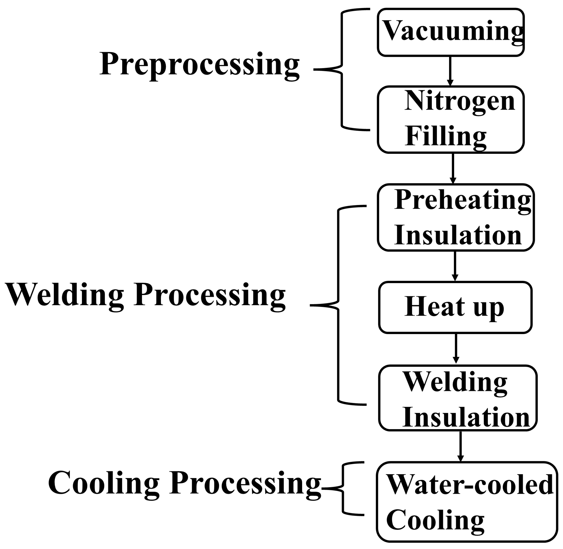
For the entire vacuum eutectic welding process, its flow chart is shown in Figure 2 below. The sample was placed in a eutectic furnace, and steps concerning vacuuming, nitrogen filling, preheating insulation, temperature rises, welding insulation and water cooling were followed. The substrate and the pad were placed in glassware, the substrate was cleaned using ultrasonic waves, the pad was cleaned using plasma cleaner, and the cleaned substrate and pad were packaged within two hours.
According to the parameters of Sn60Pb40, it could be seen that the melting point was 183 °C, the temperature set in the vacuum eutectic furnace should be higher than the melting point temperature of the soldered piece, and the welding time was 60 s or less. The sample would be a eutectic test; the final determination of the welding temperature was 220 °C, the welding time was 30 s, and the pressure was fixed at 50 g. As shown in Table 2, the process curve temperature T (°C), time CT (s), pressure F (g), vacuum V (Pa) and whether to fill the furnace with nitrogen N2 were variables set before the formal welding was set to the process curve for the empty run once, as well as before the temperature in the furnace was down to room temperature to begin welding.
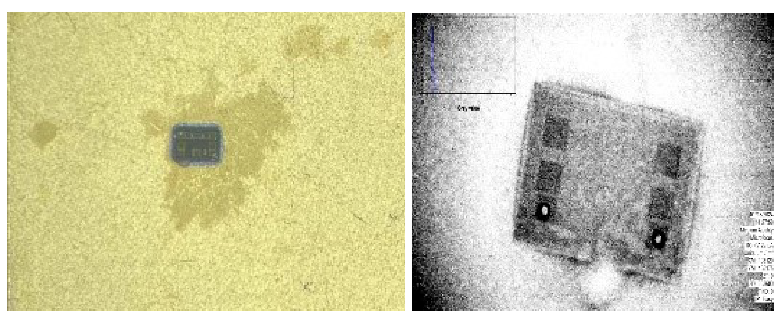
The welding experiments were carried out according to the welding process curve, and a welded sample and void rate X-ray are shown in Figure 3. The welded samples were complete with no obvious defects, and the voiding rate was tested to be less than 15%.
According to the parameters of Au80Sn20, the melting point is 280 °C. The welding temperature was finally determined to be 320 °C, with a welding time of 45 s, and the pressure was fixed at 50 g. Table 3 shows the process curve temperature T (°C), time CT (s), pressure F (g), vacuum V (Pa) and whether or not to fill with nitrogen N2.
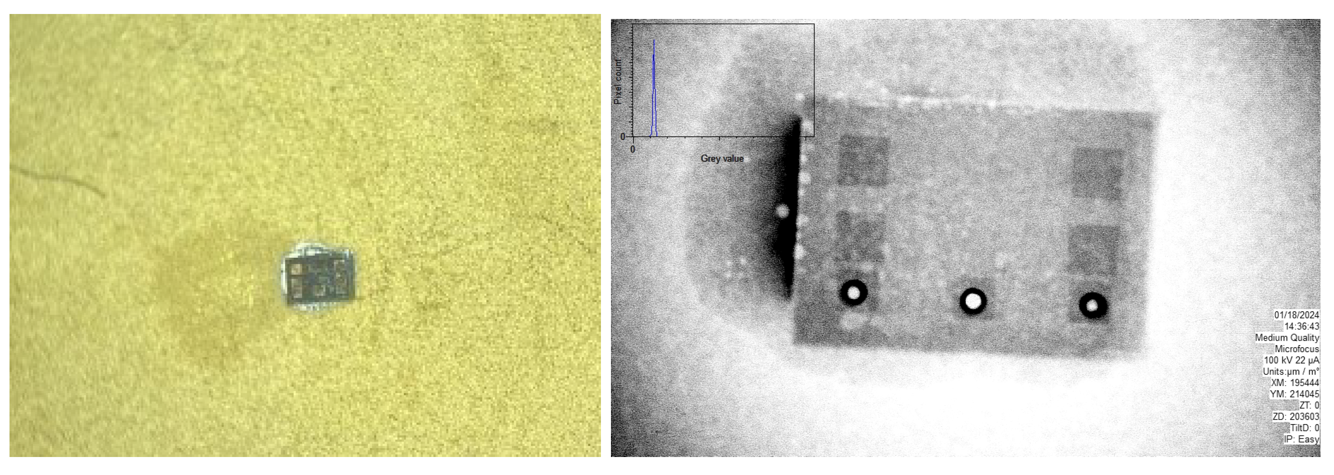
According to the welding process curve for the welding experiments, the sample after the welding and the void rate X-ray are shown in Figure 4. The welded state under the welding process curve is complete, and the void rate detection was less than 15%.
According to the parameters of Sn96.5Ag3.5, the melting point was 221 °C. The welding temperature was finally determined to be 240 °C, the welding time was 30 s, and the pressure was fixed at 50 g. Table 4 shows the process curve temperature T (°C), time CT (s), pressure F (g), vacuum V (Pa) and whether or not to fill with nitrogen N2.
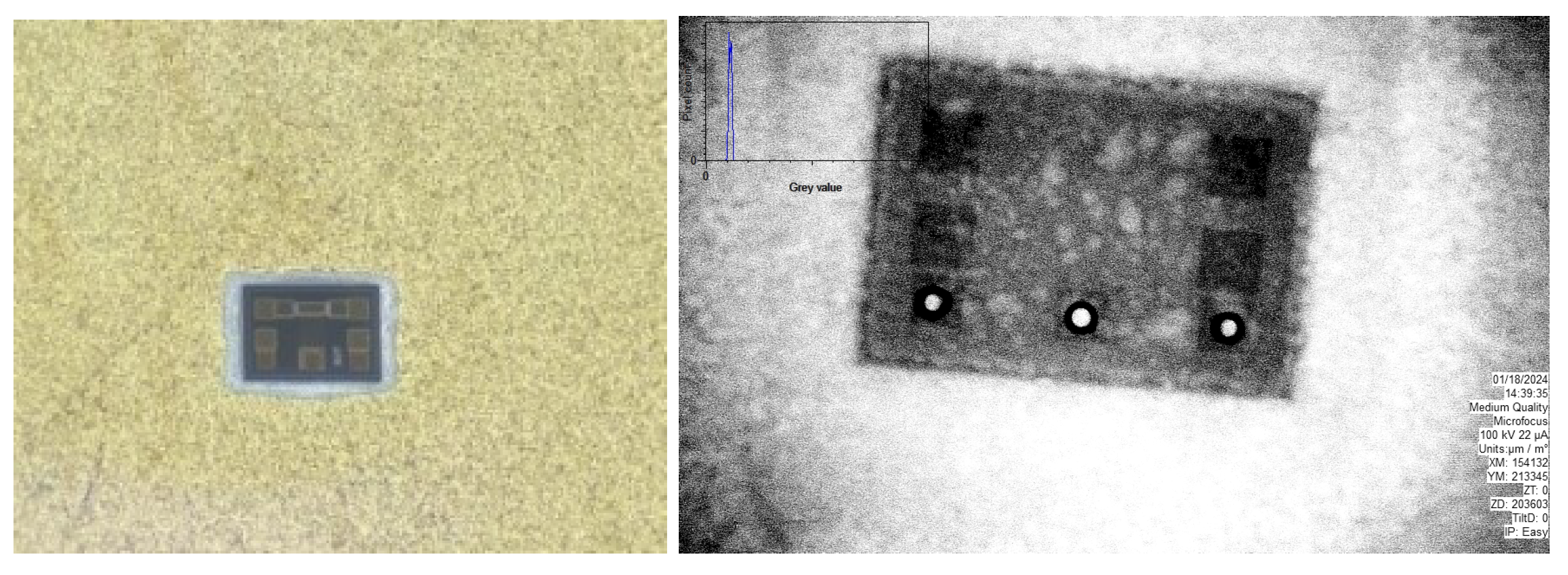
The welding experiments were carried out according to the welding process curve, and a post-welding sample and a void rate X-ray are shown in Figure 5. The welded state was complete, nwith o gaps, and the void rate detection was less than 15%.

2.3. Nano-Silver Sintering Experiments

The nano-silver sintering process refers to the use of nano-silver to form a layer of interconnected material between the chip and the substrate. In utilizing the high-temperature hot-melt properties of the nano-silver particles, through conditions such as elevated temperature sintering, chemical changes occur within the nano-silver to form a firm bond between the nano-silver particles and the metal surface. During the sintering process, the state of the nano-silver changes from a liquid to a solid, creating reliable mechanical, electrical and thermal functionality. The specific sintering method of nano-silver is as follows. (1) Pretreatment: the surface of the substrate to be welded is cleaned and polished to ensure surface finish and cleanliness. (2) Spot-coating nano-silver: nano-silver is placed on the cleaned substrate with a 0.01 mm dispensing needle. (3) Temperature baking: the samples are placed in an electric thermostat blast-drying oven and kept at 200 °C for 120 min, and under a certain temperature and time for heat treatment, in order to make the nano-silver fully melt and flow with the metal surface to form a strong bond. (4) Cool down: the melted nano-silver is left to cool down to room temperature for 60 min after taking it out of the oven to complete the welding. As shown in Figure 6 below, there was no obvious defect in the welding, and the void rate was less than 15% in the test.

3. Performance Testing and Analysis

3.1. Performance Testing

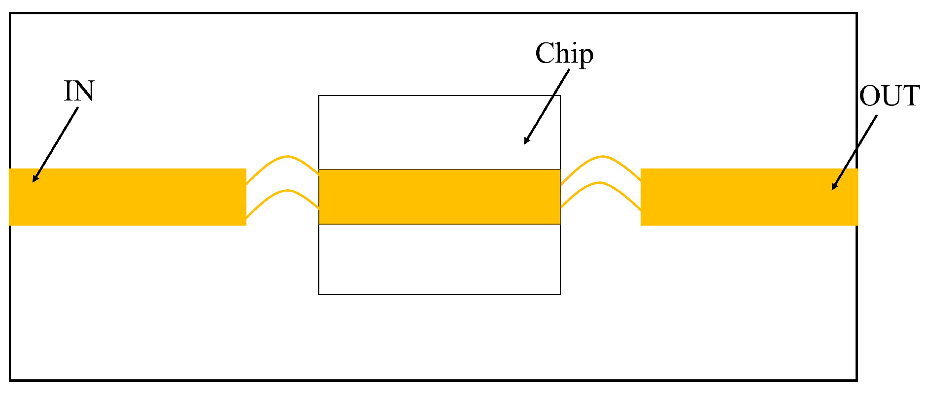
In order to simplify the model, this study utilized bonding alloy wires to make the input/output ports of the chip connected to a 50 ohm microstrip line, and the input/output signals were used to test the effects of each state of the chip after soldering on the microassembly solder. The dielectric substrate was selected from Rogers RO4003C, the microstrip line was made of nickel-plated copper plating, the bonding wire was made of gold wire with a diameter of 0.025 mm, the middle part simulated the straight-through transmission of a GaAs chip, and the upper layer of the chip was a microstrip line with 50 ohm of impedance. Figure 7 below shows the modeling diagram of the bonding established using Ansys HFSS 2022 software.
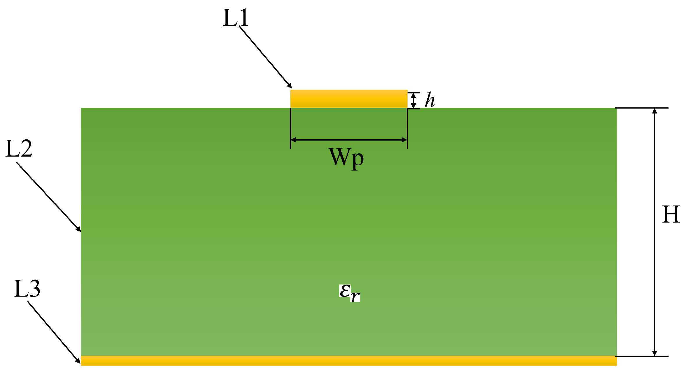
It is important to note that when the thickness h and width wp of the microstrip line are varied, the characteristic impedance of the microstrip line changes for the same relative dielectric constant. A large number of researchers have found that the microstrip line’s characteristic impedance is only related to the width of the microstrip line’s wp, the thickness of the microstrip line h and the relative dielectric constant, and the following specific formula has been proposed [15,16].
If wp/h < 2, then the microstrip line thickness wp is as shown in Equation (1):
w p = ( 8 e A h ) / ( e 2 A 2 ) ,
where the coefficient A is shown in Equation (2):
A = 2 π Z 0 / Z f ( ( ϵ r + 1 ) / 2 ) + ( ϵ r 1 ) / ( ϵ r + 1 ) ( 0.23 + 0.11 / ϵ r ) ,
If wp/h > 2, then the microstrip line thickness wp is as shown in Equation (3):
w p = 2 h / π { B 1 l n ( 2 B 1 ) + ( ϵ r 1 ) / ( 2 ϵ r ) [ l n ( B 1 ) + 0.93 0.61 / ϵ r ] } ,
where the coefficient B is shown in Equation (4):
B = ( π Z f ) / ( 2 Z 0 ( ϵ r ) ) ,
The Rogers RO4003C dielectric substrate with a relative dielectric constant of 3.4 and a thickness of h = 0.20 mm was used as the test plate designed in this study. Therefore, according to Equations (12) and (13), the line width Wp = 0.41 mm and thickness h = 0.20 mm using a 50 ohm microstrip line were calculated. The relative dielectric constant of the GaAs chip was 12.9, and the line width Wp = 0.03 mm and thickness h = 0.10 mm using the 50 ohm microstrip line were calculated through computer-aided calculations, as can be seen in Figure 8 and Table 5 below.
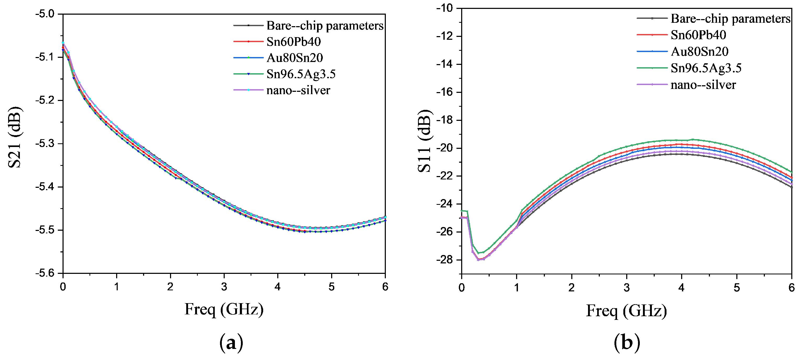
In this design of the test board for testing the electrical performance, a double-bonding span with a 0.8 mm height and the 0.05 mm bonding method were selected. After selecting a suitable bonding method, an insertion loss and return loss simulation was carried out for different packaging materials to understand the effect of the different packaging materials on the microwave performance of the whole chip after the packaging was completed. As can be seen in Figure 9 below, in the DC-6 GHz band, the error of the Au80Sn20 and silver nanomaterials in the insertion loss (S21) with the whole band of the unencapsulated state was less than 0.001 dB, and the error of the whole band of the unencapsulated state was less than 1 dB under the return loss (S11), while the Sn60Pb40 and Sn96.5Ag3.5 solders had errors of less than 0.02 dB from the unencapsulated state across the band at the insertion loss (S21) and less than 2 dB from the unencapsulated state across the band at the return loss (S11).
According to the simulation design of the test board, a suitable plate and bonding method were selected, and the CAD drawings of the test board were processed. After the processing of the test board was completed, the packaged attenuation 5 dB chip was placed in the middle groove of the microstrip line, and the input and output terminals of the chip were double bonded. Figure 10 below shows the completed test board and the completed chip-bonding effect.

3.2. Analysis of Results

The fabricated test board was connected to the vector network analyzer using coaxial cable, and the main parameter indicators were the S21 and S11 of the attenuation chip, as shown in Figure 11 below, which compares the parameter indicators of the four different encapsulation materials with the performance of the unencapsulated bare chip.
As the attenuation circuit is composed of different resistors, the resistivity of different packaging materials in the encapsulation process is different, resulting in the resistance of the signal transmission being affected, so different packaging materials have a certain impacts on the parameters of the attenuation chip. Specifically, these impact are as follows: insertion loss in four states (S21) in Au80Sn20 and nano-silver in the 0–1 GHz band (and the bare chip parameters reach the same values); in the 1–6 GHz band, the error is less than 0.003 dB; and the Sn60Pb40 and Sn96.5Ag3.5 soldering state errors in the entire test frequency band were less than 0.02 dB. The return loss (S11) values in Au80Sn20, Sn60Pb40 and nano-silver were basically consistent with the parameters of the die in the frequency band of 0–1 GHz; the error was less than 1 dB in the 1–6 GHz band; and the error was less than 2 dB in the whole frequency band for Sn96.5Ag3.5.

4. Conclusions

In this study, Sn60Pb40, Au80Sn20, Sn96.5Ag3.5 and nano-silver were selected to research the microwave performance of attenuated chip encapsulation. Samples with a low connection resistance, high heat transfer efficiency, complete packaging and a low void rate were obtained through a vacuum eutectic process and nano-sintering process. Aiming at the heat generated through insertion loss, which leads to high temperature rises in the chip, the low-insertion-loss packaging technology was innovatively studied. In designing microwave performance test boards, the performance parameters of the attenuated chips encapsulated in different packaging technologies were tested. The results show that in the DC-6 GHz band, the insertion loss of the attenuated chips after nano-silver packaging was the lowest and that the Au80Sn20 and nano-silver materials reduced the insertion loss of the chip by 85% and the return loss by 50 % compared with Sn60Pb40 and Sn96.5Ag3.5. The packaging of a low-insertion-loss attenuated chip can effectively control the temperature rise and improve the reliability of the attenuating chip package.

Author Contributions

Conceptualization, S.Y. and Z.W.; methodology, S.Y. and Z.W.; software, Z.W.; validation, S.Y., Z.W. and P.W.; formal analysis, Z.W.; investigation, Z.W.; resources, Z.W.; data curation, Z.W. and P.W.; writing—original draft preparation, Z.W.; writing—review and editing, S.Y. and P.W.; visualization, Z.W.; supervision, S.Y.; project administration, S.Y.; funding acquisition, S.Y. and P.W. All authors have read and agreed to the published version of the manuscript.

Funding

This research received no external funding.

Data Availability Statement

All data that were referenced can be found in this paper.

Conflicts of Interest

The authors declare no conflicts of interest.

References

  1. Jung, D.Y.; Jang, H.G.; Cho, D.; Park, K.S.; Lim, J.W.; Choi, Y.H.; Lee, Y. Multi-layer Ceramic Based Surface Mount Device Packaging for 1200 V and 1700 V SiC SBD Power Semiconductors. In Proceedings of the 2020 IEEE International Conference on Consumer Electronics, Las Vegas, NV, USA, 4–6 January 2020; pp. 65–68. [Google Scholar]
  2. Du, Y.; Qiao, Y.; Ren, X.; Lai, Y.; Zhao, N. Characterization of Sn-xIn Solders and Thermomigration-Induced Interfacial IMC Growth of Cu/Sn-xIn/Cu Micro Solder Joints. Electronics 2023, 12, 1899. [Google Scholar] [CrossRef]
  3. Luyang, Z. Brief analysis of micro-assembly technology of electronic products. Shandong Ind. Technol. 2015, 6, 191. [Google Scholar]
  4. Na, C.Y.; Jeon, B.M.; Kim, J.W.; Jung, W.S.; Jeong, J.S.; Cho, S.M.; Park, H.S. Fabrication of 30 µm Sn Microbumps by Electroplating and Investigation of IMC Characteristics on Shear Strength. Electronics 2022, 12, 144. [Google Scholar] [CrossRef]
  5. Chen, C.; Gong, W.; Qi, J. Research progress on chip assembly reliability and testing methods. Electron. Process. Technol. 2015, 36, 253–256. [Google Scholar]
  6. Zhou, B.; Lu, T.; You, J. Study on fatigue ductility coefficient and life prediction for mixed solder joints under thermal cycle loads. In Proceedings of the 2014 10th International Conference on Reliability, Maintainability and Safety (ICRMS), Guangzhou, China, 6–8 August 2014; pp. 686–690. [Google Scholar]
  7. Xiang, L.; Shao, L.; Yan, T. Research on low void welding of semiconductor power module chips. Equip. Manuf. Technol. 2017, 2, 82–85. [Google Scholar]
  8. Depiver, J.A.; Mallik, S.; Amalu, E.H. Characterizing Solder Materials from Random Vibration Response of Their Interconnects in BGA Packaging. J. Electron. Mater. 2023, 52, 4655–4671. [Google Scholar] [CrossRef]
  9. Lee, J.R.; Chong, M.X.; Abdul Aziz, M.S.; Khor, C.Y.; Mohd Salleh, M.A.; Mohd Arif Zainol, M.R.; Ani, F.C. Numerical Analysis of the Thermal and Mechanical Performance of Cu Pillar Bumps During Reflow: Effects of Height and Solder Material. J. Electron. Mater. 2024, 53, 1169–1182. [Google Scholar] [CrossRef]
  10. Craton, M.T.; Konstantinou, X.; Albrecht, J.D.; Chahal, P.; Papapolymerou, J. A Chip-First Microwave Package Using Multimaterial Aerosol Jet Printing. IEEE Trans. Microw. Theory Tech. 2020, 68, 3418–3427. [Google Scholar] [CrossRef]
  11. Hao, D.; Zhang, W.; Liu, X.; Liu, Y. A Wideband 6-Bit Digital Attenuator in a GaAs pHEMT MMIC. Electronics 2022, 11, 2166. [Google Scholar] [CrossRef]
  12. Yuan, H.; Yuan, Y.; Zhan, H. Effect and regulation of solder voids on the reliability of power devices. Electron. Packag. 2023, 23, 15–22. [Google Scholar]
  13. Zhou, Q.; Li, Q.; Zhou, Y. Reliability soldering study of small size Sn63Pb37 and Sn3.0Ag0.5Cu solder balls. Electron. Process. Technol. 2018, 39, 79–83+100. [Google Scholar]
  14. Jia, Q.; Zou, G.; Zhang, H. Progress of sintered connections with nanoparticle materials as intermediate layers and their encapsulation applications. J. Mech. Eng. 2022, 58, 2–16. [Google Scholar]
  15. Wang, D.Q. Research and Design of SIW Filter and Duplexer Based on Multimode Technology; Nanjing University of Posts and Telecommunications: Nanjing, China, 2022. [Google Scholar]
  16. Zuoyong, D. Research on Microwave Functional Module Micro-Assembly Application Technology. Master’s Thesis, Nanjing University of Science and Technology, Nanjing, China, 2014. [Google Scholar]
Figure 1. Overall view of the model.
Electronics 13 01785 g001
Figure 2. Vacuum eutectic welding flow chart.
Electronics 13 01785 g002
Figure 3. Sn60Pb40 post-soldering samples and void rate detection.
Electronics 13 01785 g003
Figure 4. Au80Sn20 post-soldering samples and void rate detection.
Electronics 13 01785 g004
Figure 5. Sn96.5Ag3.5 samples after soldering and void rate detection.
Electronics 13 01785 g005
Figure 6. Curing diagram of nano-silver paste.
Electronics 13 01785 g006
Figure 7. Model diagram of double-bonded alloy wire interconnected with microstrip line.
Electronics 13 01785 g007
Figure 8. Microstrip design drawing.
Electronics 13 01785 g008
Figure 9. Comparison of microwave performances of different solders: (a) simulation of model S21 with different solders; (b) simulation of model S11 with different solders.
Electronics 13 01785 g009
Figure 10. Enlarged view of fabricated test board and chip bonding.
Electronics 13 01785 g010
Figure 11. Actual measurement and analysis diagram: (a) measured parameter S21 (b); measured parameter S11.
Electronics 13 01785 g011
Table 1. Material parameters of the encapsulation model.
MakingsDensity (g/cm3)Coefficient of Thermal Expansion (10−6/°C)Thermal Conductivity (W/mk)Young’s Modulus (GPa)Poisson’s RatioConductivity (1/ohm × m)Resistivity (ohm × m)
GaAs5.325.946800.292 × 10−610−8
Sn60Pb408.5255134.50.46.1 × 10−722.4 × 10⁻⁸
Au80Sn2014.71657680.414.5 × 10−716.4 × 10⁻⁸
Sn96.5Ag3.57.43033118.70.384.7 × 10−721.3 × 10⁻⁸
nano-silver-2215018-6.62 × 10−75 × 10−8
Mo85Cu15104.81601100.345.71 × 10−71.72 × 10⁻⁸
Table 2. Process curve settings.
Serial NumberT (°C)CT (S)V (Pa)F (g)N2
1502090,000500
2506010500
315024080,000501
415012080,000501
520021080,000501
62006080,000501
72203030500
850150100,000501
Table 3. Process curve settings.
Serial NumberT (°C)CT (S)V (Pa)F (g)N2
1502090,000500
2506010500
318024080,000501
418012080,000501
530021080,000501
63006080,000501
73204530500
850150100,000501
Table 4. Process curve settings.
Serial NumberT (°C)CT (S)V (Pa)F (g)N2
1502090,000500
2506010500
314024080,000501
414012080,000501
522021080,000501
62206080,000501
72403030500
850150100,000501
Table 5. Process curve settings.
ParametersMaterial PropertiesSizes (mm)
L1Nickel-Plated Copper Plating-
L2Core RO4003C-
L3Core-
Wp-0.414
H-0.412
h-0.203
Disclaimer/Publisher’s Note: The statements, opinions and data contained in all publications are solely those of the individual author(s) and contributor(s) and not of MDPI and/or the editor(s). MDPI and/or the editor(s) disclaim responsibility for any injury to people or property resulting from any ideas, methods, instructions or products referred to in the content.