Abstract
To address the challenge of detecting small defects in Printed Circuit Boards (PCBs), a YOLO-HDEW model based on the enhanced YOLOv8 architecture is proposed. A high-resolution detection layer is introduced at the P2 feature level to improve sensitivity to small targets. Depthwise Separable Convolution (DSConv) is used for downsampling, reducing parameter complexity. An Edge-enhanced Multi-scale Parallel Attention mechanism (EMP-Attention) is integrated to capture multi-scale and edge features. The EMP mechanism is incorporated into the C2f module to form the C2f-EMP module, and dynamic non-monotonic Wise-IoU (W-IoU) loss is employed to enhance bounding box regression. The model is evaluated on the PKU-Market-PCB, DeepPCB, and NEU-DET datasets, with experimental results showing that YOLO-HDEW achieves 98.1% accuracy, 91.6% recall, 90.3% mAP@0.5, and 61.7% mAP@0.5:0.95, surpassing YOLOv8 by 1.5%, 2.3%, 1.2%, and 1.9%, respectively. Additionally, the model demonstrates strong generalization performance on the DeePCB and NEU-DET datasets. These results indicate that YOLO-HDEW significantly improves detection accuracy while maintaining a manageable model size, offering an effective solution for PCB defect detection.
1. Introduction
Modern PCB production requires high-speed, large-volume manufacturing, where undetected defects can severely affect product quality. Therefore, the detection system must not only provide rapid response capabilities, but also feature lightweight deployment to meet the needs of various production stages. Lightweight design ensures smooth integration into existing workflows, enhancing flexibility and real-time detection, thus preventing defective products from reaching the market and maintaining production efficiency and quality. PCB defects, such as open circuits, mouse bites, short circuits, burrs, and false copper, are typically small and randomly distributed. External environmental factors may also affect image clarity, making it difficult to identify defect boundaries, presenting a significant challenge for detection.
Traditional manual detection methods are inefficient and prone to errors, making them unsuitable for modern production needs [1], and automated PCB defect detection has become a key research focus. Deep learning techniques, using image processing for feature extraction and classification algorithms for defect identification, have significantly improved detection accuracy and efficiency [2,3]. Deep learning models, such as Convolutional Neural Networks (CNNs) [4], Residual Networks (ResNet) [5], and Generative Adversarial Networks (GANs) [6], have been widely applied in automated PCB defect detection. Adibhatla et al. [7] proposed a PCB defect detection method based on deep convolutional neural networks, which automatically learn features from PCB images, effectively improving defect recognition in complex backgrounds. Kaya et al. [8] combined traditional image processing techniques with deep learning methods to propose a hybrid model that effectively improves the accuracy and speed of PCB defect detection. Wu et al. [9] proposed a PCB defect detection method based on ResNet, which can accurately identify small defects in low-resolution images. Despite significant progress in deep learning methods for PCB defect detection, challenges remain in addressing issues such as imbalanced samples, detection accuracy in complex backgrounds, and model real-time performance, which are still key research topics in the future [10,11].
In recent years, YOLO has been widely used in PCB defect detection. By transforming the problem into a regression task, YOLO simultaneously predicts the object class and location, enabling fast and efficient defect localization and classification [12,13]. Huo et al. [14] proposed a real-time PCB visual inspection system based on YOLO and fuzzy logic algorithms. The system combines the YOLO algorithm for efficient object detection with fuzzy logic algorithms to optimize the accuracy of detection results, significantly improving the ability to identify small defects. Tian et al. [15] proposed an improved YOLOv3 algorithm, which enhances the model’s ability to detect small defects in complex backgrounds by introducing the DenseNet. Du et al. [16] proposed a YOLO-MBBi model, which improves the detection accuracy of complex defects by incorporating multi-channel feature fusion and adaptive bounding box regression strategies. Chen et al. [17] proposed an improved YOLOv7 algorithm based on the FasterNet backbone network and CBAM attention mechanism, which enhances the model’s sensitivity to complex defects. Yuan et al. [18] proposed an improved YOLO-HMC method that combines deep feature extraction and fine-grained feature learning, effectively improving the model’s ability to detect complex defects. Zhang et al. [19] proposed an improved YOLOv8-CM method that combines a Context Module with the YOLOv8 model, effectively enhancing the model’s performance in object detection. Huan et al. [20] introduced a GAN-enhanced YOLOv11 model for PCB defect detection, which effectively improves the model’s generalization and robustness, even with limited data. However, these algorithms lack multi-scale feature extraction and overlook edge feature information of defects, resulting in low detection accuracy for small and complex PCB defect features.
To address these challenges, we propose YOLO-HDEW, a defect detection model based on YOLOv8, designed for PCB defects with complex features and small sizes. YOLO-HDEW overcomes traditional methods’ limitations in detecting small, complex defects. It identifies hard-to-detect small defects and accurately distinguishes defect regions in complex backgrounds. Enhanced convolutional networks and feature extraction algorithms improve the clarity of defect boundaries, boosting detection accuracy and efficiency.
The main contributions of this paper are summarized as follows:
- (1)
- A high-resolution detection branch (P2) was constructed, enabling the effective fusion of shallow-layer feature maps with deep-layer feature maps within the neck network. This significantly enhances the network’s perception capability for small targets. Concurrently, Depthwise Separable Convolution (DSConv) was employed for downsampling operations, effectively reducing model parameter complexity.
- (2)
- The Edge-enhanced Multi-scale Parallel Attention mechanism (EMP-Attention) was proposed. It achieves effective feature enhancement through the multi-level collaboration of a Multi-scale Spatial Attention module, a Channel Attention module, and an Edge Feature Enhancement module.
- (3)
- The Wise-IoU (W-IoU) loss function, which integrates a dynamic non-monotonic focusing mechanism, replaces C-IoU as the updated bounding box regression loss, resulting in enhanced model detection performance.
- (4)
- Comparative experiments were conducted on the PKU-Market-PCB and DeepPCB datasets. The experimental results show that, compared to other models, YOLO-HDEW achieves higher detection accuracy.
2. Methods
2.1. YOLO-HDEW Model
The YOLO-HDEW model is shown in Figure 1. YOLO-HDEW retains the PAN-FPN network structure [21], but to avoid the loss of target features due to consecutive downsampling, a high-resolution detection branch is added to enhance the detection capability for small objects. At the same time, DSConv [22] is used for downsampling to reduce computational complexity. Additionally, an Edge-enhanced Multi-scale Parallel Attention mechanism (EMP-Attention) is constructed, which extracts multi-level features through parallel dilated convolutions and enhances high-frequency responses using an edge detection branch, thereby improving the model’s ability to capture small object features. Finally, the W-IoU [23] loss function is employed, combined with the attention mechanism and dynamic frequency modulation mechanism, to better capture and process PCB defect features.
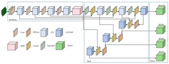
Figure 1.
YOLO-HDEW PCB defect detection module.
2.1.1. Detection Probe Improvements
- (1)
- Small target detection layer
YOLOv8’s backbone network adopts a PAN structure, progressively extracting features through multiple downsampling layers. Via successive convolution operations, the input image is incrementally downsampled to 1/8, 1/16, and 1/32 of its original size, generating corresponding feature maps P3, P4, and P5. The P3 feature map (1/8 scale) is fed into the neck network, where it integrates multi-scale features for small object detection and undergoes cross-level feature fusion.
As shown in Figure 2, the PCB dataset includes a large number of small targets. After consecutive downsampling, the features of these small targets become extremely faint in the feature maps. Particularly in complex environments, small object detection is susceptible to interference from background information, resulting in limited feature extraction.
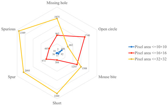
Figure 2.
The size and quantity of defect features in the PCB dataset.
Therefore, we enhanced YOLOv8 as illustrated in Figure 3. A specialized small object detection layer is incorporated into the network. By further processing shallow feature maps, a higher-resolution 1/4-scale P2 feature map is extracted for small target detection. The new small object detection probe works alongside the original detection probes, facilitating the effective fusion of shallow and deep feature maps within the neck network. This greatly enhances the network’s ability to detect small targets.
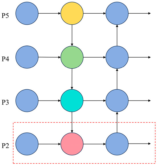
Figure 3.
Structure of the detection layer; the red dashed line highlights the newly added high-resolution detection layer P2.
The high-resolution P2 feature map retains more spatial information of small objects, which helps mitigate the issue of small object feature loss caused by consecutive downsampling. Through the optimized feature pyramid network structure, multi-scale features are efficiently fused, thereby improving the accuracy of small object detection in PCB defect detection.
- (2)
- Depthwise separable convolution
To avoid increasing the model size due to the addition of detection layers, this paper further introduces Depthwise Separable Convolution (DSConv) to replace the traditional convolutional downsampling operation with a stride of 2, as shown in Figure 4. DSConv consists of depthwise convolution and pointwise convolution. In depthwise convolution, the convolution kernel is applied independently to each input channel, generating the same number of output channels, which are then stacked along the channel dimension. The computational formula for depthwise convolution is as follows:
where i, j denote the spatial positions of the output feature map, k is the channel index, m, n denote the spatial positions of the convolution kernel, is the weight of the depthwise convolution kernel.
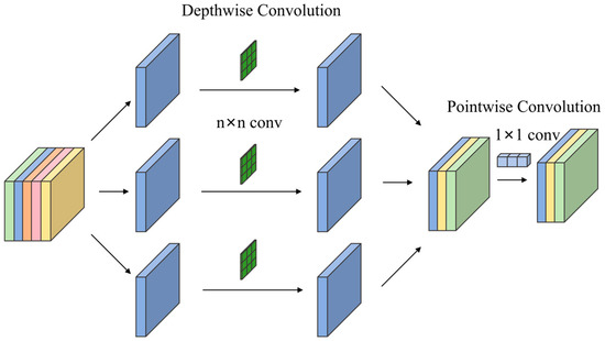
Figure 4.
Structure of DSConv.
Pointwise convolution applies 1 × 1 convolutional kernels to perform cross-channel convolution, enabling the mixing of information between channels. The computational formula for pointwise convolution is as follows:
where i, j denote the spatial positions of the output feature map, k′ is the channel index after the pointwise convolution, k is the channel indices before pointwise convolution, and is the kernel weight.
By improving the downsampling operator, the model’s parameter count is effectively reduced, while detection accuracy is enhanced and detection speed is significantly increased.
2.1.2. EMP-Attention
Attention mechanisms, widely employed in machine learning and artificial intelligence, simulate human information-processing attention allocation to automatically identify and concentrate computational resources on the most critical points within an image, thereby enhancing model comprehension and handling of complex information. Common variants include Channel Attention (CA) [24], which recalibrates channel-wise features by aggregating global spatial information; Squeeze-and-Excitation (SE) [25], which utilizes a weighting matrix to assign channel-specific importance weights; the Convolutional Block Attention Module (CBAM) [26] applies channel and spatial attention mechanisms sequentially, allowing the model to focus on both types of information.
The SE and CA methods mainly focus on channel features and global information, without optimizing edge information. However, PCB defects often exhibit distinct edge characteristics, and the absence of edge information, especially in the detection of small defects, may lead to inaccurate defect localization. Although CBAM combines both channel and spatial attention, it still has limitations when handling features at different scales, particularly in applications like PCB defect detection, where defects come in various sizes.
Inspired by these attention mechanisms, we propose EMP-Attention, which achieves effective feature enhancement through a multi-level collaborative mechanism [27]. As shown in Figure 5, it comprises three core modules: the Multi-scale Spatial Attention Module, the Channel Attention Module, and the Edge Enhancement Module. The Multi-scale Spatial Attention Module employs a parallel multi-branch architecture, implementing multi-scale dilated convolution groups F(x) with dilation rates of 1, 2, and 4. Each branch corresponds to different receptive field scales, expressed as:
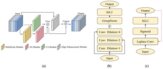
Figure 5.
(a) EMP-Attention Module; (b) MultiScale Module; the ‘~’ represents the three convs proceeding with the subsequent operation concurrently; (c) Edge Enhancement Module; The red dotted-line represents the edge_ratio.
The convolution kernel with a dilation rate of 1 covers the smallest receptive field, capturing local features in the image and aiding in the detection of fine details of small defects. The convolution kernel with a dilation rate of 2 expands the receptive field to a medium scale, which helps detect medium-sized defect features and capture local contextual information. When the dilation rate is 4, the receptive field is maximized, enabling the perception of a broader area, which helps identify global context features and the distribution range of defects. The module first extracts features at different scales using multi-branch dilated convolutions, and then performs feature concatenation along the channel dimension, achieving multi-scale feature fusion to generate a composite feature map, as shown in Figure 5a. The output feature is:
Finally, a spatial attention mechanism is introduced to automatically learn optimal scale combinations. To simultaneously capture local details of micro-defects and the global context of macro-defects, spatial attention generates a spatial weight map based on multi-scale fused features:
The channel attention module employs a two-layer 1 × 1 convolution to replace traditional fully connected layers. While compressing computational load, it dynamically learns inter-channel dependencies through global average pooling and nonlinear mapping:
In the edge feature enhancement module, we treat the image as a two-dimensional discrete function. By computing the derivative of this function, the image gradient can be obtained. Gradients reflect changes in image gray-level values, representing textural features. To preserve richer texture information, the Laplacian operator is adopted as the edge generation method to acquire coarse edge images, as shown in Figure 5b. The Laplacian operator can be expressed as:
where E is the edge image obtained by summing the second-order partial derivatives in the horizontal and vertical directions. Compared to edge extraction operators such as Sobel, Prewitt, and Canny, the edge image derived from this gradient method preserves more accurate edge feature information. To enhance the extracted edge features, we design an edge enhancement operator R, which dynamically adjusts the output via an adaptive coefficient α based on feedback from the output feature information. When obvious edge features are extracted, α increases, enhancing the features of these edge regions. Conversely, if no distinct edges are present or the edges are weak, α decreases, reducing the effect of edge enhancement:
where P denotes the input feature, α is the edge_ratio, σ is the sigmoid function, and E is the Laplacian response value.
EMP-Attention enhances the ability to recognize complex defects by combining the multi-scale channel attention module, channel attention module, and edge enhancement module. The model can dynamically adjust the feature weights of the input data, improving detection accuracy and effectively optimizing computational efficiency. Through the collaborative work of the spatial attention mechanism and edge enhancement module, the model not only extracts local features of small defects in detail but also captures the global contextual information of larger defects, significantly improving detection accuracy.
2.1.3. Improvement of C2f
The C2f module, as a core component of YOLOv8’s backbone network, significantly enhances feature extraction capabilities through its multi-branch structure. By introducing multi-branch gradient flow paths and residual connections, it effectively alleviates the vanishing gradient problem in deep networks and facilitates the fusion of shallow detail features with deep semantic features. This achieves a favorable balance between accuracy and efficiency in object detection tasks. However, its performance remains limited in dense small object detection scenarios.
To enhance the module’s feature processing ability, especially for small object representation, we incorporate the EMP-Attention mechanism before the split operation in the C2f module. This module specifically enhances small object detection by focusing on critical details and suppressing redundant information to optimize the post-split feature maps. This significantly strengthens the module’s selectivity and processing efficiency for small target features.
The improved C2f-EMP module effectively boosts the model’s small object detection performance and overall accuracy. Figure 6 illustrates the architectures of the original C2f module and the enhanced C2f-EMP module.
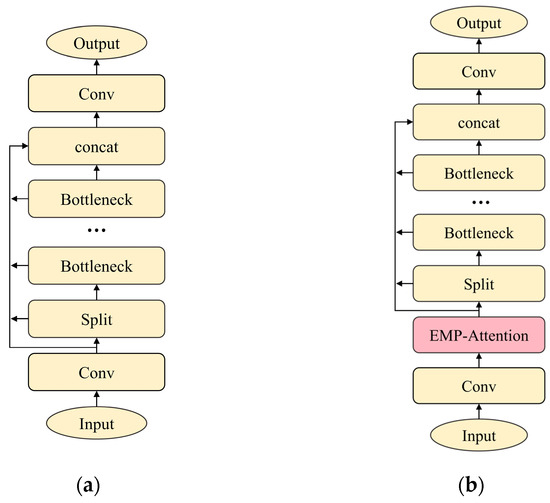
Figure 6.
The module structure of C2f-EMP before and after improvement. (a) Structure of C2f; (b) structure of C2f-EMP.
2.1.4. W-IoU
Intersection over Union (IoU) is a commonly used metric for evaluating the overlap between the predicted and ground truth bounding boxes in object detection. It measures similarity by calculating the ratio of the intersection to the union of the predicted and ground truth boxes. A higher IoU value indicates better alignment between the model’s predictions and the actual annotations, as illustrated in Figure 7. During training, IoU is often incorporated into the loss function to help optimize the model’s accuracy, allowing the model to perform more precisely in object detection tasks.
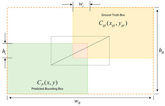
Figure 7.
Schematic diagram of loss calculation based on IoU.
YOLOv8 uses C-IoU as its loss function, which not only considers the distance, overlap, and size of the bounding box center, but also introduces an aspect ratio term. However, C-IoU performs poorly when facing real-world data with inconsistent annotation quality, especially in PCB defect detection, where there is a significant difference in the annotation quality of different defects. To improve the robustness of bounding box regression, W-IoU introduces the concept of “outlierness” and adjusts the loss penalty intensity through a dynamic gradient allocation mechanism. W-IoU adaptively adjusts the gradient weights of samples based on the IoU value between the predicted and ground truth boxes. For high-quality annotations, it enhances the gradient, while for low-quality annotations, it reduces their weight, thereby minimizing noise interference. This mechanism reduces overfitting to low-quality annotations, improves generalization ability, accelerates model convergence, and enhances detection accuracy. Therefore, W-IoU is chosen as the new bounding box loss function.
The loss function of W-IoU is calculated as follows:
3. Results
3.1. Subsection
The dataset used in this experiment is the PKU-Market-PCB dataset [28], which contains six types of defects: open circuits (Oc), short (Sh), Missing hole (Mh), Mouse bite (Mb), Spur (Sp), and Spurious copper (Sc), totaling 693 images, as shown in Figure 8. To simulate the complex scenarios that may occur in actual PCB detection, image augmentation is performed through rotation, scaling, cropping, contrast adjustment, adding noise, and other methods. Each augmentation selects two enhancement techniques, ensuring that each technique appears with equal frequency to maintain a balanced class distribution, thus avoiding the impact of class imbalance on model training. The dataset is expanded to 10,395 images, with the augmented images shown in Figure 9.
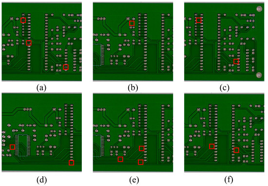
Figure 8.
Six types of PCB defect images. (a) Open circuit; (b) Short; (c) Missing hole; (d) Mouse bite; (e) Spur; (f) Spurious copper.
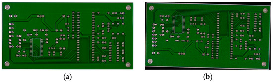
Figure 9.
Example of Image Enhancement. (a) Original image; (b) Enhanced image.
3.2. Experimental Setup
In this study, the experiments were conducted on a system running Windows 11, equipped with 16 GB of RAM, an NVIDIA RTX 4060 GPU (NVIDIA Corporation, Santa Clara, CA, USA), and an AMD Ryzen 7 CPU (Advanced Micro Devices, Sunnyvale, CA, USA). The software environment includes Torch 1.12.1 with cu113, managed through Anaconda.
Table 1 summarizes the parameter configurations used for the training process. Before training, the dataset images and corresponding labels were divided into training, validation, and test sets in a ratio of 8:1:1. The training process is set to run for a maximum of 300 epochs, and the learning rate is adjusted using the SGD optimization method. The starting learning rate is 0.01, and input images are resized to 640 × 640 for normalization.

Table 1.
Model training hyperparameter settings.
3.3. Evaluation Indicators
The evaluation metrics include Mean Average Precision (mAP), Precision (P), and Recall (R). The equations for P and R are shown in (14) and (15).
TP denotes the count of bounding boxes that were correctly predicted, FP indicates the number of positive samples incorrectly identified, and FN refers to the number of objects that were missed. Average Precision (AP) quantifies the model’s overall accuracy, whereas mAP is the average of AP values calculated across all categories. Here, k represents the total number of classes. The equations for calculating AP and mAP are provided below. We use mAP@0.5 to evaluate basic detection performance at a single IoU threshold, while mAP@0.5:0.95 provides a more comprehensive assessment by averaging precision across multiple IoU thresholds, offering a more robust measure of model performance across varying detection challenges.
3.4. Analysis of Experimental Results
3.4.1. Ablation Experiments
To assess the effectiveness of the model introduced in this study, an ablation experiment setup was proposed, as shown in Table 2. In addition, Figure 10, Figure 11, Figure 12, Figure 13 and Figure 14 show the visualization of training loss and performance metrics for both YOLOv8 and YOLO-HDEW, illustrating the improved stability of the enhanced model.
Table 2.
Ablation protocol.
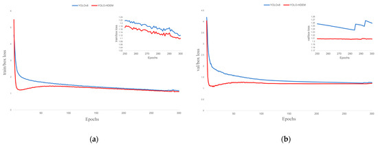
Figure 10.
Training loss performance. (a) Train box loss; (b) Val box loss.
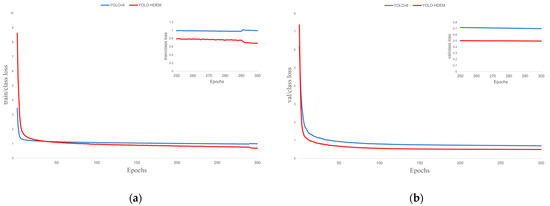
Figure 11.
Training loss performance. (a) Train class loss; (b) Val class loss.
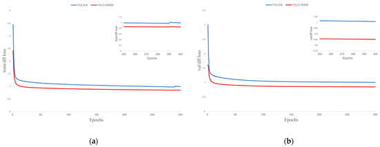
Figure 12.
Training loss performance. (a) Train dfl loss; (b) Val dfl loss.
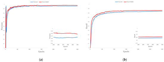
Figure 13.
Training performance. (a) Precision; (b) Recall.
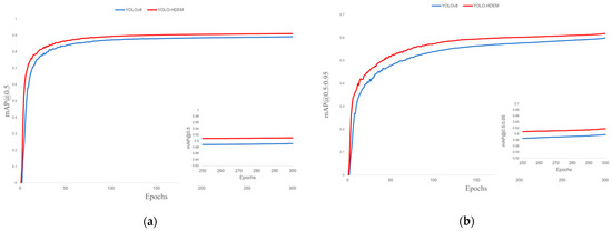
Figure 14.
Training performance. (a) mAP@0.5; (b) mAP@0.5:0.95.
The ablation experiment results are shown in Table 2. To effectively extract shallow small-target details and localization information, preventing missed detections, the P2 layer was added, and accuracy, recall, mAP@0.5, and mAP@0.5:0.95 increased by 0.3%, 0.8%, 0.3%, and 0.7%, respectively. To reduce the model’s parameter count, DSConv was introduced; although accuracy decreased by 0.1%, the number of parameters was reduced by 17%, and FPS increased by 4.9. To optimize the model’s feature fusion ability and reduce false positives, the EMP attention mechanism was added; accuracy, recall, mAP@0.5, and mAP@0.5:0.95 increased by 0.8%, 1.9%, 1.0%, and 1.4%, respectively. To make the model focus on defect details, W-IoU was introduced; accuracy, recall, mAP@0.5, and mAP@0.5:0.95 increased by 0.5%, 0.8%, 0.6%, and 1.3%, respectively. Combining P2 with DSConv effectively reduced the model size and improved detection speed while enhancing model performance. Further adding the EMP attention mechanism resulted in an additional improvement in detection accuracy while maintaining manageable model size. Finally, the YOLO-HDEW model constructed with W-IoU achieved significant improvements in accuracy, recall, mAP@0.5, and mAP@0.5:0.95, increasing by 1.5%, 2.3%, 1.2%, and 1.9%, respectively, with only a slight increase in parameters and model size. The model size is just 7.1 MB, and the FPS reached 76.9, demonstrating the effectiveness and practicality of the improved model.
The loss function of the YOLO model is composed of bounding box loss, dfl loss, and classification loss. The bounding box loss evaluates the model’s accuracy in localizing the target’s center coordinates and predicting the dimensions of the bounding box; the dfl loss evaluates the accuracy of the model’s confidence prediction regarding the presence of target objects in preset bounding boxes; the classification loss assesses the model’s discriminative performance in identifying target categories. As shown in Figure 10, Figure 11 and Figure 12, the proposed YOLO-HDEW exhibits consistently lower loss values during training compared to YOLOv8, demonstrating significant performance optimization. YOLO-HDEW’s loss function converges markedly faster, reaching lower loss values within the same training epochs. This indicates that the improved model learns features more efficiently during optimization, accelerating training efficiency. Moreover, YOLO-HDEW’s loss curve shows a smoother declining trend with significantly reduced fluctuations, reflecting enhanced stability in gradient updates during training. This avoids entrapment in local optima and mitigates gradient oscillation issues, demonstrating YOLO-HDEW’s superior generalization capability to stably capture essential data characteristics. As shown in Figure 13 and Figure 14, YOLO-HDEW outperforms in accuracy, recall, mAP@0.5, and mAP@0.5:0.95, validating the model’s enhanced precision for PCB defect detection.
3.4.2. Comparative Test
- (1)
- Comparative Experiments of Different Attention Mechanisms
To assess the effectiveness of EMP, we conducted comparative experiments using YOLOv8n as the baseline model. We integrated SE, CA, and CBAM at the same position as EMP while keeping other parameters consistent. The experimental results are presented in Table 3.
Table 3.
Different attention contrast experiment table.
Compared with the YOLOv8n model, all attention mechanisms improved precision. Among various attention mechanisms, EMP achieved the highest mAP@0.5 and mAP@0.5:0.95 at 90.7% and 61.9%, respectively. This improvement is mainly attributed to the introduction of the edge enhancement module, which enables the model to be more precise in localizing small defects. Although CA showed 0.2% higher precision than EMP, its recall, mAP@0.5, and mAP@0.5:0.95 were lower by 0.2%, 1.0%, and 0.2%, respectively. This indicates that the design of multi-scale channel attention enhances the model’s ability to recognize different types of defects, while the spatial attention module further strengthens the focus on defect regions. These results demonstrate the effectiveness and feasibility of EMP in PCB defect detection tasks.
To visually demonstrate the effectiveness of EMP, GradCAMPlusPlus was used to create heatmaps of the feature extraction regions, as shown in Figure 15. From the figure, it can be observed that the features extracted by the original method are scattered across various regions of the image, wasting computational resources and inevitably leading to insufficient attention to some defect targets. In contrast, the regions focused on by EMP are more concentrated and contain more representative and important information. This allows the model to more quickly locate and identify target categories in the image, eliminate areas that do not belong to the target categories, and improve detection accuracy by capturing richer semantic information.
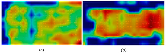
Figure 15.
Heatmap comparison of feature extraction capabilities. (a) YOLOv8n; (b) YOLOv8n + EMP.
- (2)
- Comparison experiments of different loss functions
In order to evaluate the effectiveness of the W-IoU loss function, comparative experiments were conducted using the G-IoU [29], E-IoU [30], and S-IoU [31] loss functions. The experimental results are shown in Table 4.
Table 4.
Different loss function contrast experiment table.
As shown in Table 4, the W-IoU loss function adopted in this study demonstrates significant improvements over the baseline model’s C-IoU loss function. Specifically, it increases mAP@0.5 by 1.2%, mAP@0.5:0.95 by 0.1%, precision by 1.1%, and recall by 2.5%. This demonstrates that W-IoU is better suited for PCB defect detection tasks.
- (3)
- Comparison experiments of various models
To evaluate YOLO-HDEW’s detection performance for tiny targets under complex environmental interference, we selected six state-of-the-art YOLO-series algorithms (YOLOX-tiny, YOLOv3, YOLOv5, YOLOv7, YOLOv8, YOLOv11) and Faster R-CNN, TDD-Net [32] for comparative experiments with our improved YOLOv8 model. Experimental results of these algorithms on the augmented PCB dataset are shown in Table 5.
Table 5.
Comparison of advanced object detection algorithms.
In terms of model performance, YOLO-HDEW achieves 90.3% mAP@0.5 and 61.7% mAP@0.5:0.95, representing increases of 1.2% and 1.9%, respectively, compared to YOLOv8n. With detection precision and recall reaching 98.1% and 91.6%, YOLO-HDEW outperforms other algorithms. Complexity comparison shows YOLO-HDEW maintains 3.461M parameters without significant growth, attributable to replacing downsampling modules with DSConv in the neck network. Although the volume of YOLOX-Tiny is 0.9 MB smaller than YOLO-HDEW and its FPS is 5.8 higher, its detection accuracy is significantly lower than that of YOLO-HDEW. This indicates that YOLO-HDEW possesses the ability for lightweight deployment and fast detection, making it an ideal lightweight model for the PCB detection industry’s demand for efficient solutions. Comparative results demonstrate YOLO-HDEW’s superior average detection metrics for PCB defects and significantly improved detection accuracy versus mainstream models.
3.4.3. Model Performance Validation
To evaluate the practical detection performance of the model, PCB surface defect detection was carried out on both the original and the improved models. Figure 16 illustrates the detection results across various defect categories, where red or yellow markers indicate detected defects with labeled accuracy scores. Row (a) shows original PCB images, row (b) displays YOLOv8 detection results, and row (c) presents YOLO-HDEW detection results. As demonstrated in Figure 12, YOLO-HDEW outperforms YOLOv8 in all six PCB defect categories, indicating enhanced detection accuracy for diverse defects and effective reduction of misjudgments and missed detections.
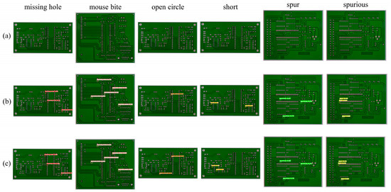
Figure 16.
Validation results for YOLO-HDEW and YOLOv8. (a) Original image; (b) Detected by YOLOv8; (c) Detected by YOLO-HDEW.
To more clearly demonstrate the model’s improvements, Figure 17 presents zoomed-in views of the detection results, highlighting the enhanced detection accuracy of YOLO-HDEW in identifying small and complex defects. In contrast, Figure 18 illustrates how YOLO-HDEW effectively avoids false negatives, successfully detecting defects that YOLOv8 missed. These results emphasize the model’s improved precision and its ability to minimize both false positives and false negatives.
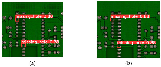
Figure 17.
Accuracy improvement of zoomed-in detection results. (a) YOLOv8 detection results; (b) YOLO-HDEW detection results.
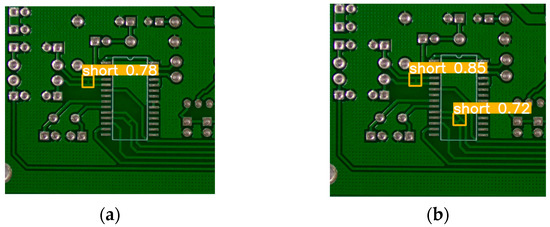
Figure 18.
False negative improvement zoomed-in detection results. (a) YOLOv8 detection results; (b) YOLO-HDEW detection results.
3.4.4. Experimental Results of DeepPCB
To validate the generalization performance of the model, we expanded our evaluation by incorporating another publicly available grayscale image dataset, DeepPCB. The images were captured using a linear-scan Charge-Coupled Device (CCD), resulting in a dataset containing 1500 images with a resolution of 640 × 640 pixels. The defect types align with the PKU-Market-PCB dataset, including six distinct defect categories, whose distributions are shown in Figure 19.
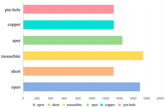
Figure 19.
Number of defect categories.
Comparative experiments were conducted using Faster R-CNN, TDD-Net, YOLOX-tiny, YOLOv3, YOLOv5, YOLOv7, YOLOv8, YOLOv11, and our improved YOLOv8 model, with results detailed in Table 6. As shown in Table 6, the YOLO-HDEW model achieves 97.3% precision, 97.1% recall, 98.9% mAP@0.5, and 80.1% mAP@0.5:0.95 on the DeepPCB dataset. While its precision is slightly lower than YOLOv11, all other metrics surpass those of comparative models. These results confirm that YOLO-HDEW excels not only on PKU-Market-PCB, but also on DeepPCB, further validating the algorithm’s effectiveness. Selected test results from the improved model are displayed in Figure 20.
Table 6.
Comparison of advanced object detection algorithms.
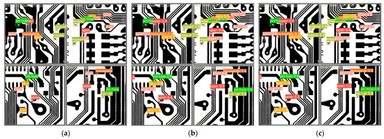
Figure 20.
Defect detection results on the DeepPCB. (a) Original image; (b) Detected by YOLOv8; (c) Detected by YOLO-HDEW.
3.4.5. Experimental Results of NEU-DET
To further validate the generalization ability of the model, we integrated the steel surface defect dataset created by Northeastern University. This dataset contains 1800 images, covering six common types of steel surface defects: Crazing (Cr), Inclusion (In), Patches (Pa), Pitted Surface (Ps), Rolled-in Scale (Rs), and Scratches (Sc). The resolution of these images is 200 × 200 pixels, with 300 images for each defect type. Comparative experiments were conducted using Faster R-CNN, TDD-Net, YOLOX-tiny, YOLOv3, YOLOv5, YOLOv7, YOLOv8, YOLOv11, and our improved YOLOv8 model, with results shown in Table 7. The YOLO-HDEW model achieved 68.3% accuracy, 74.5% recall, 83.5% mAP@0.5, and 49.0% mAP@0.5:0.95 on the NEU-DET dataset, performing slightly lower in recall compared to YOLOv8, but surpassing the other models in the remaining metrics. These results indicate that YOLO-HDEW demonstrates good generalization on the NEU-DET dataset.
Table 7.
Comparison of advanced object detection algorithms.
To further evaluate the model’s practical detection performance, surface defect detection on steel was performed using both the pre-improved and post-improved models, with the test results shown in Figure 21. In this figure, row (a) shows the original steel images, row (b) shows the detection results of the YOLOv8 model, and row (c) shows the detection results of the YOLO-HDEW model. From the detection results shown in Figure 21, it can be observed that YOLO-HDEW outperforms YOLOv8 in detecting cracks, spots, rolled-in scale, and scratches, indicating that the improved model enhances the detection accuracy across different defect categories. However, it also shows false negatives in detecting inclusions and misclassifies a good region as a defect when identifying pitted surfaces. This suggests that while YOLO-HDEW has improved, it still faces significant challenges in detecting defects without fixed shapes or boundaries.
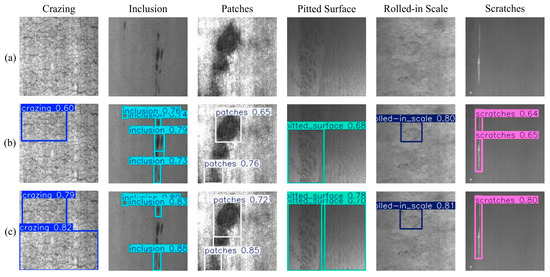
Figure 21.
Defect detection results on the NEU-DET. (a) Original image; (b)Detected by YOLOv8; (c) Detected by YOLO-HDEW.
4. Conclusions
To address the challenge of low precision in PCB defect detection, this paper proposes the YOLO-HDEW model. First, a shallow-resolution P2 layer is introduced to prevent loss of small-target features caused by excessive downsampling, while DSConv is adopted for downsampling operations to mitigate parameter growth from added detection layers and reduce redundant parameters. Second, the enhanced EMP module in the neck network integrates global and local information, enabling superior capture of fine-grained small-target features. Its dynamic weight generation mechanism adaptively adjusts channel-wise weight allocation, improving multi-scale adaptability while suppressing background noise from shallow features to prioritize target regions. Finally, W-IoU replaces the baseline C-IoU as the bounding box loss function, enhancing small-target detection capability. Comparative experiments demonstrate YOLO-HDEW’s superiority over mainstream models in resolving false positives and missed detections, while achieving higher precision and faster inference speed that meet lightweight deployment requirements. Consequently, YOLO-HDEW fulfills industrial standards for PCB surface defect inspection, providing significant theoretical and practical references for object detection algorithms in industrial quality inspection.
The comparative experimental results on the PKU-Market-PCB dataset show that YOLO-HDEW achieves better detection accuracy and speed, meeting the requirements for lightweight deployment. In summary, YOLO-HDEW provides important theoretical support and practical reference for object detection algorithms in the industrial quality inspection field. Generalization experiments on the DeepPCB and NEU-DET datasets validate the model’s generalization ability, but performance remains suboptimal when detecting defects without fixed shapes or boundaries. Future work will focus on cross-dataset collaborative learning to improve performance in diverse scenarios. Additionally, defect detection and recognition for images with varying quality and resolution will be a key direction for future optimization.
Author Contributions
Conceptualization, C.S. and Y.Z.; methodology, Y.Z.; software, Y.Z.; investigation, Y.M., Q.Q. and Z.W.; resources, C.S.; writing—original draft preparation, Y.Z.; writing—review and editing, Y.Z.; visualization, Y.Z.; supervision, K.H.; funding acquisition, C.S. All authors have read and agreed to the published version of the manuscript.
Funding
This research was funded by the National Natural Science Foundation of China (NSFC), grant number 61902205, project manager Keyong Hu.
Data Availability Statement
PKU-Market-PCB: https://robotics.pkusz.edu.cn/resources/dataset/ (accessed on 22 August 2025). DeepPCB: https://github.com/tangsanli5201/DeepPCB (accessed on 22 August 2025).
Acknowledgments
We would like to thank the editor and the anonymous reviewers for their valuable feedback. We also appreciate the contributions of everyone who supported this research.
Conflicts of Interest
The authors declare no conflicts of interest.
References
- Ren, Z.; Liu, Y.; Zhang, J.; Wang, X.; Li, C. State of the Art in Defect Detection Based on Machine Vision. Int. J. Precis. Eng. Manuf.-Green Technol. 2022, 9, 661–691. [Google Scholar] [CrossRef]
- Tulbure, A.-A.; Tulbure, A.-A.; Dulf, E.-H. A Review on Modern Defect Detection Models Using DCNNs–Deep Convolutional Neural Networks. J. Adv. Res 2022, 35, 33–48. [Google Scholar] [CrossRef] [PubMed]
- Zhou, Y.; Yuan, M.; Zhang, J.; Ding, G.; Qin, S. Review of vision-based defect detection research and its perspectives for printed circuit board. J. Manuf. Syst. 2023, 70, 557–578. [Google Scholar] [CrossRef]
- Zhang, D.; Chen, Y.; Li, M.; Liu, Z.; Wei, H. An Efficient Lightweight Convolutional Neural Network for Industrial Surface Defect Detection. Artif. Intell. Rev. 2023, 56, 10651–10677. [Google Scholar] [CrossRef]
- Zhang, H.; Jiang, L.; Li, C. CS-ResNet: Cost-Sensitive Residual Convolutional Neural Network for PCB Cosmetic Defect Detection. Expert Syst. Appl. 2021, 185, 115673. [Google Scholar] [CrossRef]
- He, X.; Chang, Z.; Zhang, L.; Xu, H.; Chen, H.; Luo, Z. A survey of defect detection applications based on generative adversarial networks. IEEE Access 2022, 10, 113493–113512. [Google Scholar] [CrossRef]
- Adibhatla, V.A.; Shieh, J.S.; Abbod, M.F.; Chih, H.C.; Hsu, C.C.; Cheng, J. Detecting Defects in PCB Using Deep Learning via Convolution Neural Networks. In Proceedings of the 13th International Microsystems, Packaging, Assembly and Circuits Technology Conference (IMPACT), Taipei, Taiwan, 24–26 October 2018; IEEE: Piscataway, NJ, USA, 2018. [Google Scholar]
- Kaya, G.U. Development of hybrid optical sensor based on deep learning to detect and classify the micro-size defects in printed circuit board. Measurement 2023, 206, 112247. [Google Scholar] [CrossRef]
- Wu, L.; Zhang, L.; Zhou, Q. Printed circuit board quality detection method integrating lightweight network and dual attention mechanism. IEEE Access 2022, 10, 87617–87629. [Google Scholar] [CrossRef]
- Jiang, W.; Li, Q.; Zhou, Y.; He, X. PCB Defects Target Detection Combining Multi-Scale and Attention Mechanism. Eng. Appl. Artif. Intell. 2023, 123, 106359. [Google Scholar] [CrossRef]
- Tang, H.; Li, Z.; Zhang, D.; He, S.; Tang, J. Divide-and-Conquer: Confluent Triple-Flow Network for RGB-T Salient Object Detection. IEEE Trans. Pattern Anal. Mach. Intell. 2025, 47, 1958–1974. [Google Scholar] [CrossRef]
- Redmon, J.; Divvala, S.; Girshick, R.; Farhadi, A. You only look once: Unified, real-time object detection. In Proceedings of the IEEE Conference on Computer Vision and Pattern Recognition (CVPR), Las Vegas, NV, USA, 27–30 June 2016. [Google Scholar]
- Han, X.; Chang, J.; Wang, K.J.P.C.S. You only look once: Unified, real-time object detection. Procedia Comput. Sci. 2021, 183, 61–72. [Google Scholar] [CrossRef]
- Huo, X. Development of a real-time Printed Circuit board (PCB) visual inspection system using You Only Look Once (YOLO) and fuzzy logic algorithms. J. Intell. Fuzzy Syst. 2023, 45, 4139–4145. [Google Scholar] [CrossRef]
- Tian, Y.; Zhang, Z.; Liu, X.; Sun, S.; Hu, J. Apple Detection During Different Growth Stages in Orchards Using the Improved YOLO-V3 Model. Comput. Electron. Agric. 2019, 157, 417–426. [Google Scholar] [CrossRef]
- Du, B.; Wan, F.; Lei, G.; Xu, L.; Xu, C.; Xiong, Y. YOLO-MBBi: PCB surface defect detection method based on enhanced YOLOv5. Electronics 2023, 12, 2821. [Google Scholar] [CrossRef]
- Chen, B.; Dang, Z. Fast PCB defect detection method based on FasterNet backbone network and CBAM attention mechanism integrated with feature fusion module in improved YOLOv7. IEEE Access 2023, 11, 95092–95103. [Google Scholar] [CrossRef]
- Yuan, M.; Zhou, Y.; Ren, X.; Zhi, H.; Zhang, J.; Chen, H. YOLO-HMC: An improved method for PCB surface defect detection. IEEE Trans. Instrum. Meas. 2024, 73, 1–11. [Google Scholar] [CrossRef]
- Zhang, C.; Li, H.; Sun, G.; Li, Y.; Liu, Z. Automated Detection and Segmentation of Tunnel Defects and Objects Using YOLOv8-CM. Tunn. Underground Space Technol. 2024, 150, 105857. [Google Scholar] [CrossRef]
- Huang, J.; Zhao, F.; Chen, L. Defect Detection Network in PCB Circuit Devices Based on GAN Enhanced YOLOv11. arXiv 2025, arXiv:2501.06879. [Google Scholar] [CrossRef]
- Liu, S.; Qi, L.; Qin, H.; Shi, J.; Jia, J. Path aggregation network for instance segmentation. In Proceedings of the IEEE Conference on Computer Vision and Pattern Recognition, Salt Lake City, UT, USA, 18–23 June 2018; pp. 8759–8768. [Google Scholar]
- Khan, Z.Y.; Niu, Z. CNN with Depthwise Separable Convolutions and Combined Kernels for Rating Prediction. Expert Syst. Appl. 2021, 170, 114528. [Google Scholar] [CrossRef]
- Tong, Z.; Chen, Y.; Xu, Z.; Yu, R. Wise-IoU: Bounding box regression loss with dynamic focusing mechanism. arXiv 2023, arXiv:2301.10051. [Google Scholar]
- Guo, M.-H.; Zhang, F.; Li, J.; Xie, Y. Attention Mechanisms in Computer Vision: A Survey. Comput. Vis. Media 2022, 8, 331–368. [Google Scholar] [CrossRef]
- Jin, X.; Yang, M.; Zhang, L.; Wei, Y.; Liu, J. Delving Deep into Spatial Pooling for Squeeze-and-Excitation Networks. Pattern Recognit. 2022, 121, 108159. [Google Scholar] [CrossRef]
- Woo, S.; Park, J.; Lee, J.-Y.; Kweon, I.S. CBAM: Convolutional block attention module. In Proceedings of the European Conference on Computer Vision (ECCV), Munich, Germany, 8–14 September 2018. [Google Scholar]
- Zhang, F.; Zhang, Z. IEAM: Integrating Edge Enhancement and Attention Mechanism with Multi-Path Complementary Features for Salient Object Detection in Remote Sensing Images. Remote Sens. 2025, 17, 2053. [Google Scholar] [CrossRef]
- Huang, W.; Wei, P.; Zhang, M.; Liu, H. HRIPCB: A challenging dataset for PCB defects detection and classification. J. Eng. 2020, 2020, 303–309. [Google Scholar] [CrossRef]
- Rezatofighi, H.; Tsoi, N.; Gwak, J.; Sadeghian, A.; Reid, I.; Savarese, S. Generalized Intersection Over Union: A Metric and a Loss for Bounding Box Regression. In Proceedings of the IEEE/CVF Conference on Computer Vision and Pattern Recognition (CVPR), Long Beach, CA, USA, 15–20 June 2019; pp. 658–666. [Google Scholar]
- Zhang, Y.-F.; Ren, W.; Zhang, Z.; Jia, Z.; Wang, L.; Tan, T. Focal and Efficient IOU Loss for Accurate Bounding Box Regression. Neurocomputing 2021, 506, 146–157. [Google Scholar] [CrossRef]
- Gevorgyan, Z. SIoU Loss: More Powerful Learning for Bounding Box Regression. arXiv 2022, arXiv:2205.12740. [Google Scholar] [CrossRef]
- Ding, R.; Dai, L.; Li, G.; Liu, H. TDD-net: A tiny defect detection network for printed circuit boards. CAAI Trans. Intell. Technol. 2019, 4, 110–116. [Google Scholar] [CrossRef]


Disclaimer/Publisher’s Note: The statements, opinions and data contained in all publications are solely those of the individual author(s) and contributor(s) and not of MDPI and/or the editor(s). MDPI and/or the editor(s) disclaim responsibility for any injury to people or property resulting from any ideas, methods, instructions or products referred to in the content. |
© 2025 by the authors. Licensee MDPI, Basel, Switzerland. This article is an open access article distributed under the terms and conditions of the Creative Commons Attribution (CC BY) license (https://creativecommons.org/licenses/by/4.0/).