Abstract
In the domain of printed circuit board (PCB) defect detection, challenges such as missed detections and false positives remain prevalent. To address these challenges, we propose a small-sample, high-precision PCB defect detection algorithm, called SSHP-YOLO. The proposed method incorporates an ELAN-C module that merges the convolutional block attention module (CBAM) with the efficient layer aggregation network (ELAN), thereby enhancing the model’s focus on defect features and improving the detection of minute defect details. Furthermore, we introduce the ASPPCSPC structure, which extracts multi-scale features using pyramid pooling combined with dilated convolutions while maintaining the resolution of feature maps. This design improves the detection accuracy and robustness, thereby enhancing the algorithm’s generalization ability. Additionally, we employ the SIoU loss function to optimize the regression between the predicted and ground-truth bounding boxes, thus improving the localization accuracy of minute defects. The experimental results show that SSHP-YOLO achieves a recall rate that is 11.84% higher than traditional YOLOv7, with a mean average precision (mAP) of 97.80%. This leads to a substantial improvement in the detection accuracy, effectively mitigating issues related to missed and false detections in PCB defect detection tasks.
1. Introduction
The rapid development of electronic technology has made printed circuit boards (PCBs) the basic component of electronic devices, and their performance, stability, and reliability directly affect the effectiveness of the overall equipment [1]. Therefore, PCB defect detection technology in the manufacturing of electronic products has a vital role in ensuring the stability of electronic products [2]. Traditional PCB testing methods are artificial visual examination methods, online testing, flying needle testing and so on. However, traditional manual inspection methods are highly subjective, rely on the experience and visual acuity of operators, and exhibit a high rate of misjudgments [3]. The online test method has limited detection capacity for physical defects (such as poor welding, cracks and so on). In addition, online testing equipment requires professional operations and maintenance, and the cost of use is high [4]. The flying needle test method exhibits a relatively slow speed and low efficiency when applied to large-scale, high-density, and high-precision circuit board detection. At present, these traditional detection methods find it difficult to meet the needs of modern industrial production [5]. Therefore, studying an efficient and accurate PCB deficiency detection method has become an urgent problem.
At present, the methods for PCB defect detection are mainly the following: conventional feature extraction techniques and deep learning approaches. Traditional feature extraction methods capture target information through structured steps, such as edge detection and texture analysis [6]. Acciani et al. [7] passed the geometric features extracted from the input welded image to the multi-layer perceptual machine, and then obtained the classification result. Although this method improves the overall classification rate for five types of welded defects, the reference image is obtained through multiple image-matching steps. The calculation process is complex, and it performs only defect classification without defect positioning. Annaby et al. [8] proposed an optimized and low-complexity algorithm. The algorithm belongs to the one-dimensional category; during matching, the two-dimensional sub-image is converted into a one-dimensional descriptor, and the descriptors are then transformed. The implementation of the algorithm has improved the calculation efficiency and reduced the impact of noise. However, the detection accuracy remains limited. The swift advancement of deep learning technology provides new solutions in the field of PCB defect detection [9]. Li et al. [10] leveraged the XGBoost model and neural transformation networks to capture dynamic facial and bodily features, objectively linking classroom participation to academic outcomes. While these approaches demonstrate the efficacy of multimodal fusion in assessing engagement, their application is predominantly focused on general educational settings, leaving room for further exploration in specialized domains such as PCB defect detection, where multimodal data could similarly enhance the detection accuracy and robustness. Zhang et al. [11] introduced a dual-domain feature extraction framework that combined spatial and frequency domain features, along with a resource allocation mechanism to enhance feature integration. Despite these advancements, this approach heavily relies on handcrafted mechanisms, such as channel and position attention, which may not fully adapt to diverse scenarios or exploit latent feature relationships effectively. Li et al. [12] introduced an extended characteristic pyramid network detection model, which effectively combines high-level semantic details with low-level geometric features and introduces a focus loss function. The experimental results demonstrate that the model exhibits strong transferability. However, in the actual industrial production environment, due to the problems of noise interference and uneven exposure, the accuracy is still low and the generalization ability of the algorithm is poor, which makes it unsuitable for industrial production applications. Wang et al. [13] developed a deep large-kernel backbone to broaden the effective receptive field and capture global information more efficiently. They also employed 1 × 1 convolutions to balance the model’s depth, thereby enhancing the efficiency of the feature extraction through reparameterization techniques. Furthermore, they introduced a bidirectional weighted feature fusion network, along with an innovative noise filter and feature enhancement extractor, to eliminate noise generated during information fusion and to recalibrate features across different channels, thereby improving the quality of the deep features. Additionally, the aspect ratio of the bounding box was simplified to address the issue of specificity values. Finally, they achieved an average mean average precision of 97.3% after multiple experiments. Wang et al. [14] proposed a SparseBEV-based framework for enhancing 3D object detection accuracy by incorporating a hybrid discrete–continuous loss function. This method effectively mitigates planar-stereo misidentifications and improves 3D direction regression. However, its reliance on limited contextual information and challenges in handling diverse geometries reduce its robustness in real-world applications. Song et al. [15] proposed a coordinate attention dynamic mechanism that performs convolution operations with the deformable convolutional network v2 (DCNv2) using coordinate attention based on YOLOv7 and a dynamic head diverse (Dy Head-d) module that prioritizes spatial awareness over scale awareness, building on Dy Head. Finally, the WDC-YOLO achieved a mean average precision of 98.4% on public datasets. The two algorithms have enhanced the accuracy of PCB defect detection, but they exhibit poor generalization ability, and the model training process is complicated. In the referenced study, the authors used rotation, random cropping, and other data augmentation methods to expand the original dataset to 10,668 PCB defect images, which improved the model’s performance on a common benchmark. However, this large sample demand not only increases the cost of data collection and processing but also results in significant computational overheads.
To solve the problems of the above-mentioned PCB defect detection accuracy, weak generalization ability, and complex model training, this article proposes a small-sample and high-precision PCB defect detection algorithm: SSHP-YOLO. The main work is as follows.
(1) Design a small target feature information extraction module: The ELAN-C module. The convolutional block attention module (CBAM), combined with the efficient layer attention network (ELAN), constitutes the ELAN-C Module, increasing the degree of attention to PCB tiny defect information.
(2) Propose the ASPPCSPC structure: By combining the dilated convolution, the spatial pyramid pooling and the concatenate operation, extract the multi-scale features of the PCB defects to improve the detection accuracy.
(3) Use the SIoU loss function to enhance the soft-matching relationship between the detection box and the real frame in the target detection, improving the predictive accuracy of the border box.
(4) On the PKU-MARKET-PCB public dataset, through ablation experiments, comparative experiments and visual comparison analysis, verify the effectiveness of each part of this article and the performance advantages of the proposed algorithm.
(5) On the NEU-DET public dataset, through comparative experiments, verify the generalization capacity of the proposed algorithm.
2. Related Work
The YOLO algorithm was first proposed by Joseph Redmon et al. [16] in 2015. The network structure of YOLOv1 mainly includes 24 convolutional layers and two fully connected layers. In the detection process, the image is divided into 7 × 7 grids, and each grid predicts two bounding boxes and class probabilities, and the output is a 7 × 7 × 30 tensor. YOLOv1 is superior to Faster R-CNN in terms of the detection speed and can process 45 frames per second, but the detection effect is poor for small and similar objects. The following year, Joseph Redmon et al. [17] introduced the anchor mechanism, added multi-scale training and joint training strategies, and used the Darknet-19 network structure to propose the YOLOv2 algorithm. The suggested algorithm enhances the detection precision while ensuring a quick detection rate. Then, Redmon et al. [18] made improvements based on YOLOv2 and proposed YOLOv3. The feature extraction component utilizes the Darknet-53 network architecture. The feature pyramid network (FPNLIN) [19] is used for multi-scale detection, which guarantees the precision of object detection while considering practical aspects. In 2020, YOLOv4 was proposed by Alexey Bochkovskiy et al. [20]. Several improvements were made to YOLOv3, including the use of CSPNet as the backbone network, the introduction of the Mish activation function, and the adoption of the CIoU loss function to enhance the detection performance in terms of small objects. One month after YOLOv4’s release, YOLOv5 was officially introduced. YOLOv5 optimizes both the network training and inference processes, emphasizes industrial applicability, and has become the most widely studied algorithm in surface defect detection on PCBs.
Based on YOLOv3, Ge et al. [21] developed YOLOX in 2021 by implementing methods such as decoupled head, data augmentation, anchor free, and SimOTA sample matching to create an anchor-free, end-to-end object detection framework. YOLOv6 was proposed by Li et al. [22]. The algorithm cancels the anchor box that has been used from YOLOv1 to YOLOv5, optimizes the backbone network and neck network, and decouples the detection head to separate the classification process of border and category. Wang et al. [23] proposed YOLOv7 in 2022. They reconstructed the head structure, introduced a new attention mechanism and feature fusion method, and achieved strong performance on multiple standard datasets, making it one of the most studied algorithms in the field of PCB surface defect detection. Table 1 summarizes the network structure of the YOLO family of algorithms.

Table 1.
Network structure of the YOLO family of algorithms.
In view of the problems in the field of PCB defect detection, many scholars have proposed their own methods based on YOLOv5 and YOLOv7. Du et al. [24] proposed YOLO-MBBi, using mobile inverted residual bottleneck block (MBConv) modules, CBAM attention and depth-wise convolutions to substitute layers in the YOLOv5s network. Zhou et al. [25] combined the lightweight MobileNet-v3 network with the CSPDarknet53 network and replaced the coupling detection head with a decoupling detection head. Yuan et al. [26] proposed YOLO-HMC, which adopted the backbone part the HorNet as an improved multiple, designed a convolutional block attention module, and used the content-aware reassembly of features to replace the up-sampling layer of the original model. Xiao et al. [27] introduced the coordinate attention mechanism to improve the backbone and neck network of YOLOv7-tiny, used DS-Conv to replace part of the common convolution in YOLOv7-tiny and used Inner-CIoU as the bounding box regression loss function. Luo et al. [28] proposed EC-YOLO, in which ACmix (a mixed model that enjoys the benefits of both self-attention and convolution)was used as a substitute for the 3 × 3 convolutional modules in the extended ELAN (E-ELAN) architecture, the ResNet-ACmix module was engineered, and the dynamic head (DyHead) was utilized. Multi-modality object detection, especially involving infrared and visible imagery, has drawn significant attention due to its potential to integrate complementary features for improved robustness. Zhang et al. [29] proposed an antagonistic-learning-based framework, utilizing modules like AFED for extracting differential features and ADFF for attention-based feature fusion. This method demonstrates state-of-the-art performance on infrared and visible detection benchmarks. However, its focus on large-scale datasets and general-purpose tasks makes it less effective for small-sample scenarios or domain-specific applications, such as PCB defect detection.
In the above works, some scholars have improved the accuracy of the model, some scholars have reduced the number of parameters of the model, and some scholars have improved the generalization ability of the model to a certain extent. However, these methods rely on a large number of samples, often reaching thousands or even tens of thousands, resulting in significant waste of computational resources. Therefore, SSHP-YOLO is proposed, which has strong generalization ability while ensuring the high accuracy of the model. The entry-level graphics card RTX-4060 can be used to train the model with a small sample.
3. Proposed Method
3.1. Overall Network Structure
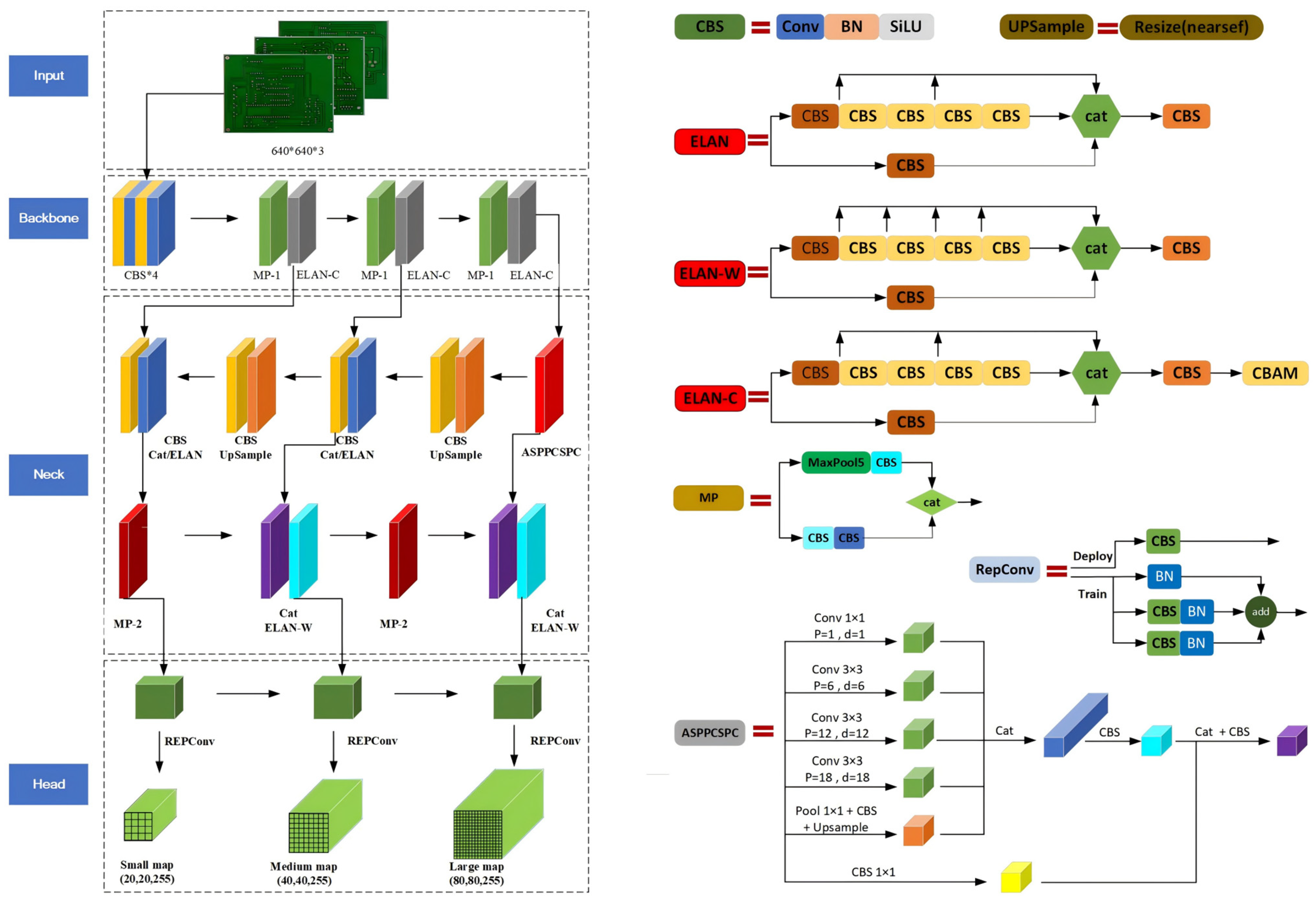
The YOLOv7 algorithm is a one-stage target detection method. Based on YOLOv7, we propose SSHP-YOLO, and the overall network structure is illustrated in Figure 1.
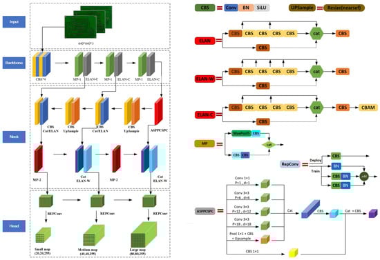
Figure 1.
SSHP-YOLO network structure.
3.1.1. Input Module
The input module preprocesses PCB defective images. The input image is unified to 640 × 640 through the resize method, ensuring that the input image is matched with the model requirements, so that it can be processed correctly through its main network.
3.1.2. Backbone Module
The backbone module is characterized by featuring the input PCB defective image and finally obtained three feature layers. The backbone network structure is mainly composed of the CBS (convolution + bn naturalization + SiLU activation function) module, MP-1 module, and ELAN-C (CBS module for multi-branch stack with CBAM) module.
3.1.3. Neck Module
The neck module enhances feature extraction, primarily incorporating ASPPCSPC, ELAN-W, UP Sample, and the Cat structure. The ASPPCSPC module employs SPP with dilated convolution and a CSP structure to expand the receptive field, facilitating feature map fusion, enriching the feature information, and aiding in the detection of PCB image defects. Compared to the ELAN module, the ELAN-W module incorporates two additional stitching operations. The UP Sample module is utilized to achieve efficient fusion of features at different levels. The Cat structure further optimizes the performance of the convolutional layers.
3.1.4. Head Module
The head module performs detection by using a high-parameter structure to determine the number of output channels, generating a prediction box, and estimating its location, confidence, and category. These predictions serve as the model’s final output.
3.2. ELAN-C Module
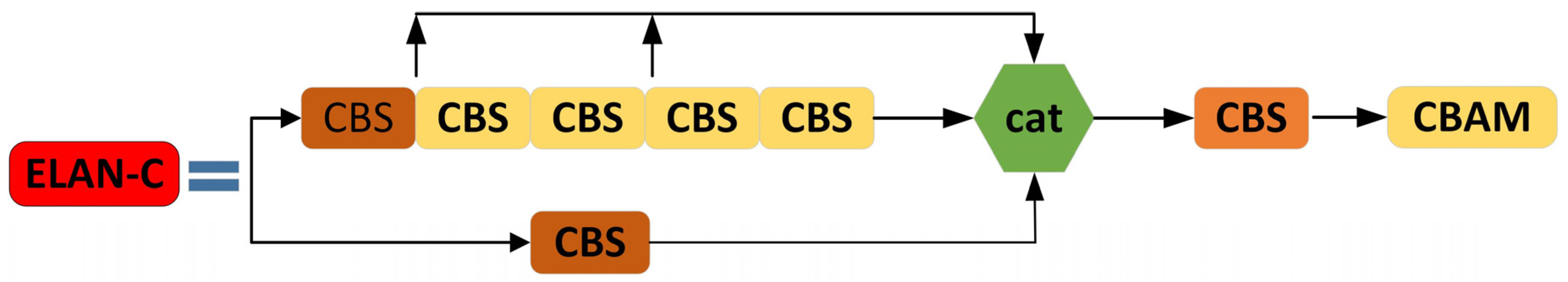
In YOLOv7, ELAN can learn complex features by effectively managing both the shortest and longest gradient pathways, demonstrating significant robustness [30]. It effectively aggregates the characteristics of different levels of characteristics, which significantly improves the model’s capture ability in terms of multi-scale target information. Especially when processing tasks with significant scale differences, it shows a strong performance advantage. Nonetheless, when it comes to identifying defects in PCBs, the detection difficulty of ELAN is still large due to small defect size and the low contrast of PCBs.
We propose a small target feature information extraction module: ELAN-C module, as shown in Figure 2. The module that adds the CBAM after the ELAN depth can decouple the convolution process, thereby constructing a new, highly efficient layer attention network. The ELAN-C module fully leverages the surrounding contextual information. By dynamically adjusting the weights of the PCB feature map, it enhances the utilization of global information and significantly improves the sensitivity to local, subtle defect details. This capability is particularly advantageous for detecting high-density, multi-detailed PCB defects, where precision in identifying subtle variations is crucial. Furthermore, the module’s ability to effectively extract and prioritize essential features reduces the reliance on large training datasets. This makes SSHP-YOLO highly data-efficient.
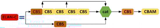
Figure 2.
ELAN-C module.
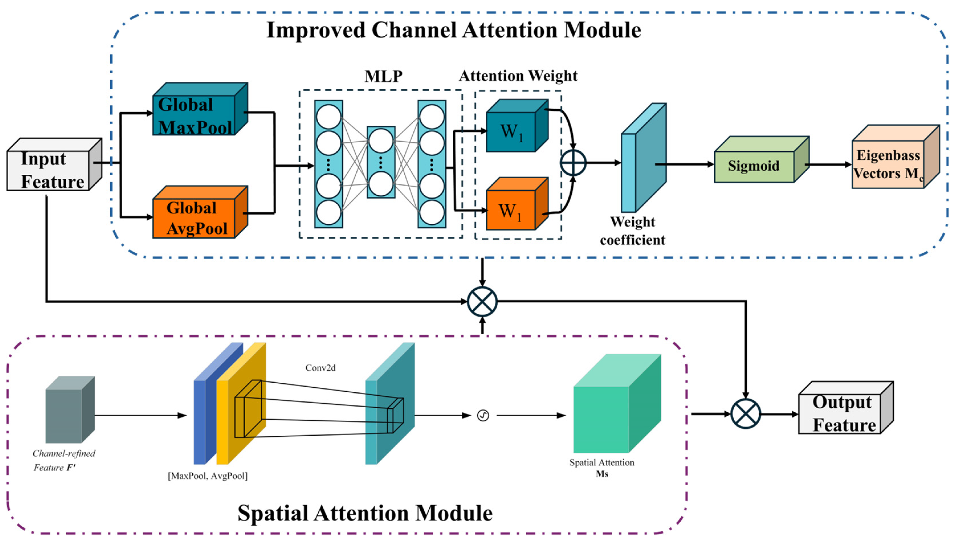
The CBAM [31] is an attention mechanism that employs dual pathways, consisting of a channel attention module (CAM) and a spatial attention module (SAM), as depicted in Figure 3.
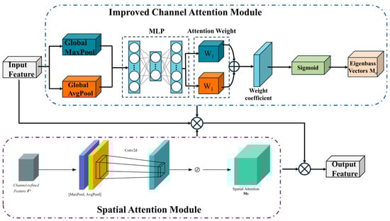
Figure 3.
Convolutional block attention module.
The CAM focuses on the channel characteristics of the PCB feature diagram. This module applies maximum pooling and average pooling to the input feature map in parallel, and then it sends the two one-dimensional tensors after pooling to the fully connected layer to obtain the channel attention weight MC. Finally, the MC is element-wise multiplied by the input feature map F to generate the feature map F’ adjusted by the CAM.
The specific calculations are shown in Equation (1).
Among them, is the average pooling, is the maximum pooling, is the weight of the hidden layer to the output layer, is the weight of the input layer to the dimension layer, is the vector after average pooling, and is the vector after maximum pooling.
The SAM focuses on the spatial characteristics of the PCB feature diagram. This module concatenates the tensors after maximum pooling and average pooling according to space, and then it performs convolution and sigmoid nonlinear activation operations in turn to normalize the channel weights of the PCB feature maps and generate the spatial attention weights MS. Finally, the MS is element-wise multiplied by the input feature map F′ to produce the feature map F″ adjusted by the SAM. The specific calculations are shown in Equation (2).
Among them, is a 2-dimensional space attention vector; is a convolutional layer that uses a convolution kernel size of 7 × 7; is average pooling, with a size of 1 × H × W; and is the maximum pooling feature, with a size of 1 × H × W.
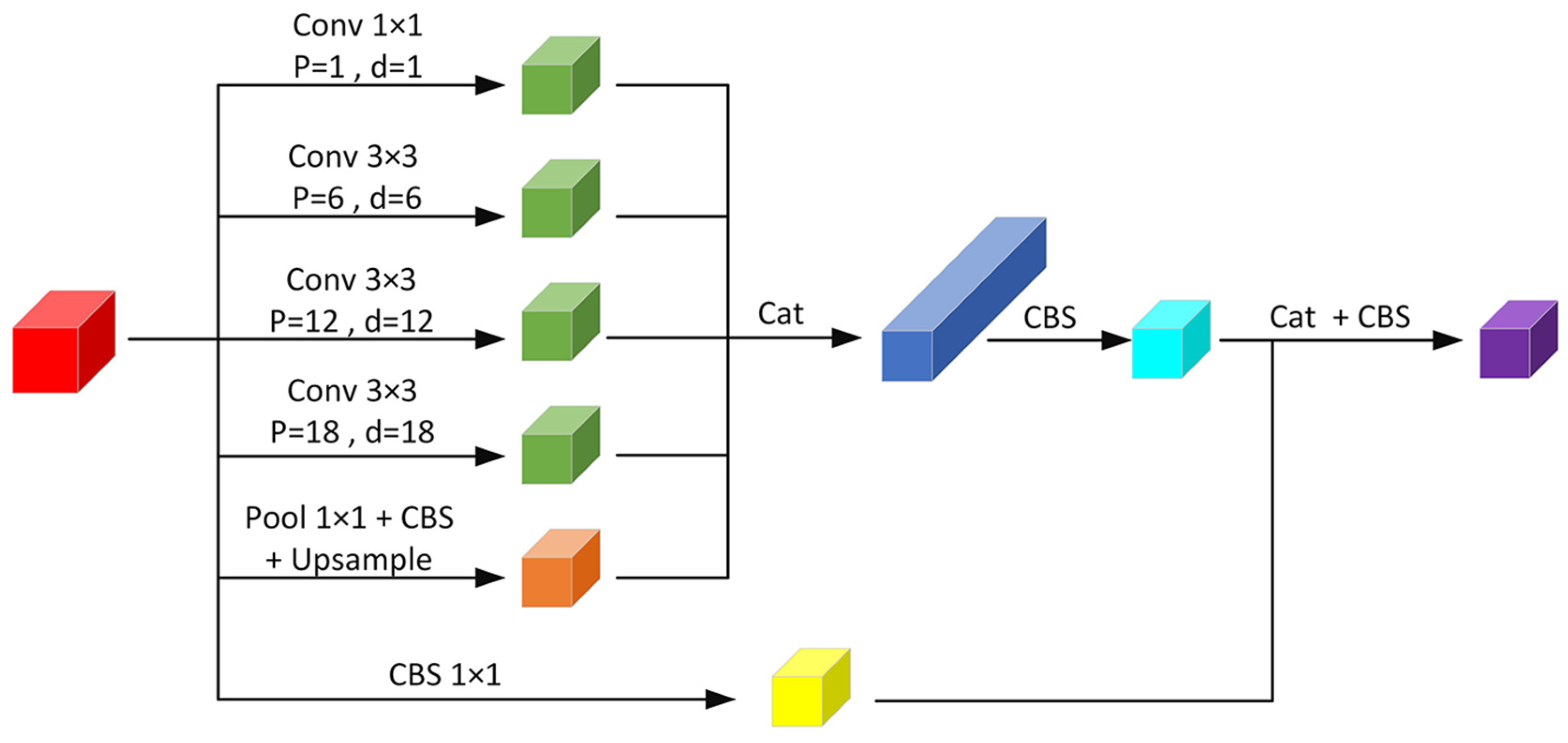
3.3. ASPPCSPC Module
In YOLOv7, the SPPCSPC structure adopts multiple branches [32], which combine the maximum pooling method of different sizes and the PCB defect characteristics obtained by conventional convolution. The processing method of scale enhances the sensitivity of the model to different size defects. By introducing the spatial pyramid pooling (SPP) layer, the SPPCSPC structure can significantly increase the effective field and enable the algorithm to capture global information more effectively, which is particularly important for identifying defects that span larger areas. However, the SPP structure inevitably leads to the loss of feature map resolution while increasing the receptive field, which will weaken the algorithm’s ability to capture fine features, thus affecting the accuracy and robustness of PCB defect detection. Resolution loss becomes a key factor limiting the detection performance, particularly when handling small defects or those with blurred edges.
The structure of the ASPPCSPC that has been suggested is illustrated in Figure 4. The dilated convolution [33] is set to ensure that the resolution of the feature map is unchanged while the receptive field is increased. The receptive field is further expanded through multiple dilated convolutions, pooling, parallel operations, and splicing, enabling multi-scale feature extraction that enhances the precision and robustness of PCB defect identification. This ensures that the network effectively captures fine details and contextual information, which is critical for detecting small or subtle PCB defects. The structure integrates multi-scale feature extraction through dilated convolution, pooling, parallel, and splicing operations, enhancing both the precision and the reliability of PCB defect identification. Dilated convolution adds the dilated rate (d) parameter to traditional convolution and adds convolution with a constant weight of 0 to the convolution kernel. The receptive field of the convolution kernel is expanded by increasing the hole step, so that each convolution operation can cover a wider input area and capture more context information. At the same time, combined with the padding operation (p), the dilated convolution can maintain the output feature map’s resolution to allow the network to effectively gather information at multiple scales. This high-resolution feature extraction reduces the reliance on large-scale annotated datasets, improving the model’s adaptability and efficiency in data-scarce environments.

Figure 4.
ASPPCSPC module.
The ASPPCSPC structure is mainly composed of the ASPP and CSP. The ASPP structure contains one 1 × 1 convolution with d of 0, which is equivalent to a normal convolution, and three 3 × 3 convolution with d of {6,12,18} and filled with p of {6,12,18}, resulting in PCB feature maps that have an equal number of input channels, height and width. In this structure, four dilated convolutions with different d are used in parallel for sampling, which effectively expands the receptive field of the feature map while maintaining the resolution of the image. This high-resolution feature enables the algorithm to precisely locate PCB defects. Moreover, the use of varying dilation rates (d) enables the network to perceive information at multiple scales, allowing for a more comprehensive understanding and analysis of details and contextual information within the image, thereby enhancing the performance of PCB defect detection. This approach is particularly advantageous for small-sample datasets, as it ensures high-quality feature representation without sacrificing detail, enabling accurate defect localization with fewer labeled samples. In parallel with the ASPP structure, image-level feature representation is performed. The specific operation is to apply global average pooling followed by a CBS structure, and then a bilinear up-sample operation is performed to generate PCB feature maps that match the quantity, height, and width of the input channels.
This enhances the capability of the feature map to extract features more effectively. The CSP structure divides the feature map into two parts. One part is processed with the ASPP structure and parallel image feature representation, and the other part is processed with traditional CBS. Finally, the CBS structure is used to output the PCB feature map using the same number of channels, as well as the same height and width of the input feature map. By leveraging these dual pathways, the ASPPCSPC structure enhances the feature extraction capability, enabling robust and precise detection of PCB defects. Moreover, this efficient architecture significantly reduces the dependency on extensive training datasets, ensuring that SSHP-YOLO performs effectively even in small-sample settings.
3.4. SIoU Loss Function
In the task of detecting targets, the boundary box loss function plays a vital role [34]. The coordinate loss in the YOLOv7 network model uses the CIoU loss function, which is calculated as in Equation (3).
Among them, represents the prediction box; means the real box; and IoU is used to overlap between the quantitative prediction box and the real frame. The higher the value, the more accurate the prediction; represents the Euclidean distance between the center of the predicted box and the true box and refers to the diagonal len10668h of the minimum rectangular closed area that can fully cover the prediction box and the real frame. The consistency ratio of the length between the prediction box and the real frame is measured, and Equation (4) is defined.
Among them, represents the width of the center position of the rear frame; represents the level of the center of the rear frame; represents the width of the position of the center of the prediction box; and is a parameter used for trade-off, which indicates the weight of the weight, defined as shown in Equation (5).
Although the CIoU loss function introduces the length–width ratio of the detection box, it can only measure the consistency of the width and height ratio. It is not the difference between the real width and height and its confidence, which will hinder the return optimization of the forecast box. The SIoU [35] loss function starts from the direction and angle between the regression vector, and it introduces the angle between the actual box and the predicted box in vector terms. The calculation is as shown in Equation (6).
Among them, is a distance loss and omega is the shape loss. The SIoU loss function makes the model converge faster by introducing the vector angle between the prediction box and the real frame. This design makes the SIoU loss function more advantageous in the target detection task, which can more accurately locate the target object, thereby improving the model’s accuracy. Therefore, this article uses the SIoU loss function.
4. Experiments and Results
4.1. Experimental Environment and Settings
This experiment uses the Python language for development, using the PyTorch deep learning framework. The specific environment and configuration are shown in Table 2.
Table 2.
Experimental environment and parameters.
4.2. Dataset
This experimental dataset uses the following public dataset: PKU-MARKET-PCB. The dataset contains 693 images, with a total of six defects. The defects and numbers are shown in Table 3.
Table 3.
Types and numbers of defects.
4.3. Evaluation Metrics
The precision (P) represents the proportion of samples that belong to the positive class in all the samples predicted as positive classes and calculates Equation (7). Among them, represents the number of samples that are correctly classified as positive samples in all the sets of all the actual samples; and represents the number of samples that are mistakenly classified as positive samples in the negative sample set. It belongs to a positive sample, and the model predicts it as the number of samples of the negative class.
The recall rate (R) indicates that in the group of positive samples, the proportion of the model’s prediction as a positive sample is calculated as in Equation (8).
The average accuracy (AP) represents the average accuracy rate of a certain class and measures the identification effect of the model for the category. The area of the curve of the horizontal axis and the vertical axis is the value of the AP. The calculation is as shown in Equation (9).
The average accuracy (mAP) refers to the average accuracy of multiple categories, that is, the average value of all the APs, and the calculation is as shown in Equation (10).
4.4. Ablation Experiment
In order to verify the effectiveness of the algorithm improvement, this article is designed to include ablation experiments. According to the different model improvements, a total of five groups of experiments are divided into five groups. The results of the ablation experiments are presented in Table 4.
Table 4.
Results of the ablation experiments.
The “√” in Table 3 indicates that the experiment incorporates this improvement, while the “×” label denotes the absence of this improvement. It can be observed that when the ELAN-C module is applied, the algorithm shows a slight increase in performance, while the P slightly is decreased, and both the R and mAP are improved. When the ASPPCSPC and SIoU are improved independently, the precision (P), recall (R), and mean average precision (mAP) of the algorithm increase. Compared to YOLOv7, SSHP-YOLO shows an increase of 2.04% in precision, 11.84% in recall, and 8.28% in mAP, demonstrating the effectiveness of the SSHP-YOLO algorithm in enhancing the individual components of YOLOv7 without mutual exclusivity among the modules.
4.5. Comparison Experiment
At present, numerous scholars have conducted extensive studies on PCB defect detection. Some researchers have applied data augmentation techniques, including flipping, rotation, scaling, noise addition, and color adjustment, to expand the PKU-Market-PCB dataset to 10,668 images, making this expanded dataset publicly available. To highlight the performance advantages of the proposed SSHP-YOLO algorithm, comparative experiments were conducted against mainstream algorithms on both the original dataset and the publicly available expanded dataset. The performance was quantified using the mAP metric, and the results of the comparison are presented in Table 5.
Table 5.
Performance comparison results of the different algorithms.
The experimental results clearly demonstrate that SSHP-YOLO delivers exceptional performance, particularly on the small-sample dataset. It achieves an impressive mAP of 97.8%, outperforming all the other algorithms evaluated on the same dataset and remaining competitive even when tested with the expanded dataset. This remarkable performance highlights SSHP-YOLO’s ability to effectively balance data constraints while achieving superior detection accuracy, solidifying its role in high-precision PCB defect detection tasks. When comparing the experimental results across algorithms, it is evident that all the other algorithms exhibit lower mAP on the small-sample dataset compared to the large-sample dataset, indicating that data augmentation techniques (e.g., flipping, rotation, scaling, noise addition, and color adjustment) improved the model’s performance. However, SSHP-YOLO not only achieves the highest mAP on the small-sample dataset (97.8%) but also surpasses the performance of the other algorithms on the large-sample datasets, underscoring its robustness and efficiency. Specifically, traditional detection algorithms, such as SSD and Faster RCNN, achieve small-sample mAP values of 78.2% and 80.1%, respectively. These relatively weak performances highlight their limited feature extraction capabilities when addressing complex PCB defect detection tasks. Single-stage detection algorithms, such as CenterNet and YOLOX, perform better, with mAP values of 89.4% and 90.2%, respectively, demonstrating the balance advantage of single-stage algorithms in terms of the speed and accuracy. Algorithms optimized for PCB defect detection, such as PCB-YOLO and TDD-Net, further improve the detection accuracy, achieving mAP values of 94.4% and 93.1%, respectively. However, they still fail to achieve the best results. The extended FPN algorithm improves the mAP to 95.0% by leveraging multi-scale feature fusion, but it still falls short of the proposed SSHP-YOLO. The proposed SSHP-YOLO algorithm significantly enhances the model’s ability to recognize small defects and subtle features, achieving the highest mAP on both the small-sample and expanded datasets. This indicates that SSHP-YOLO is not only capable of handling limited data effectively but also excels at leveraging large-scale datasets. Such performance advantages, particularly in high-precision scenarios with small samples, demonstrate its exceptional detection capabilities and establish it as a more effective solution for PCB defect detection tasks.
4.6. Visual Comparative Analysis
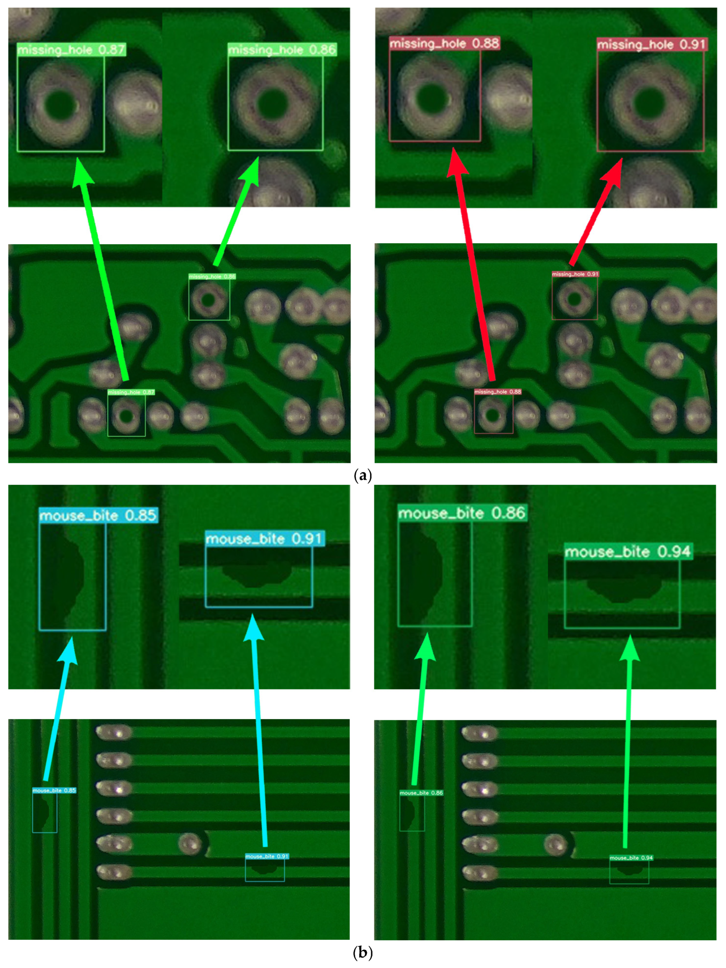
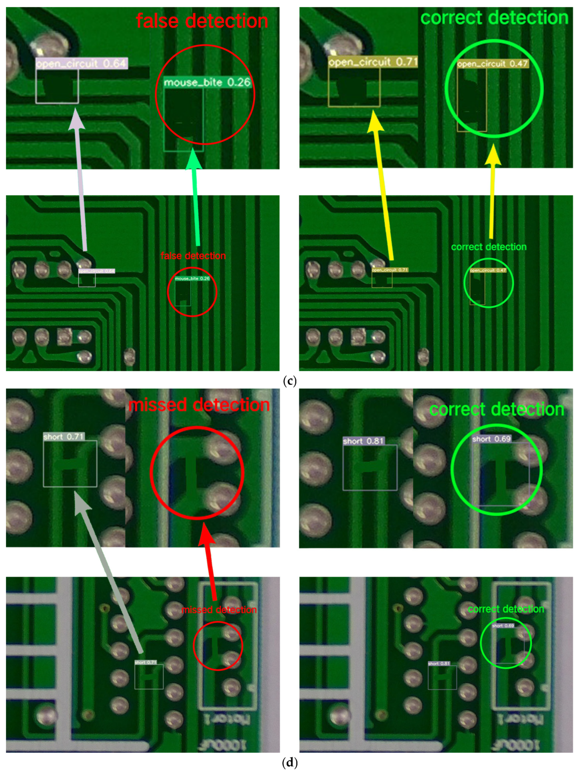
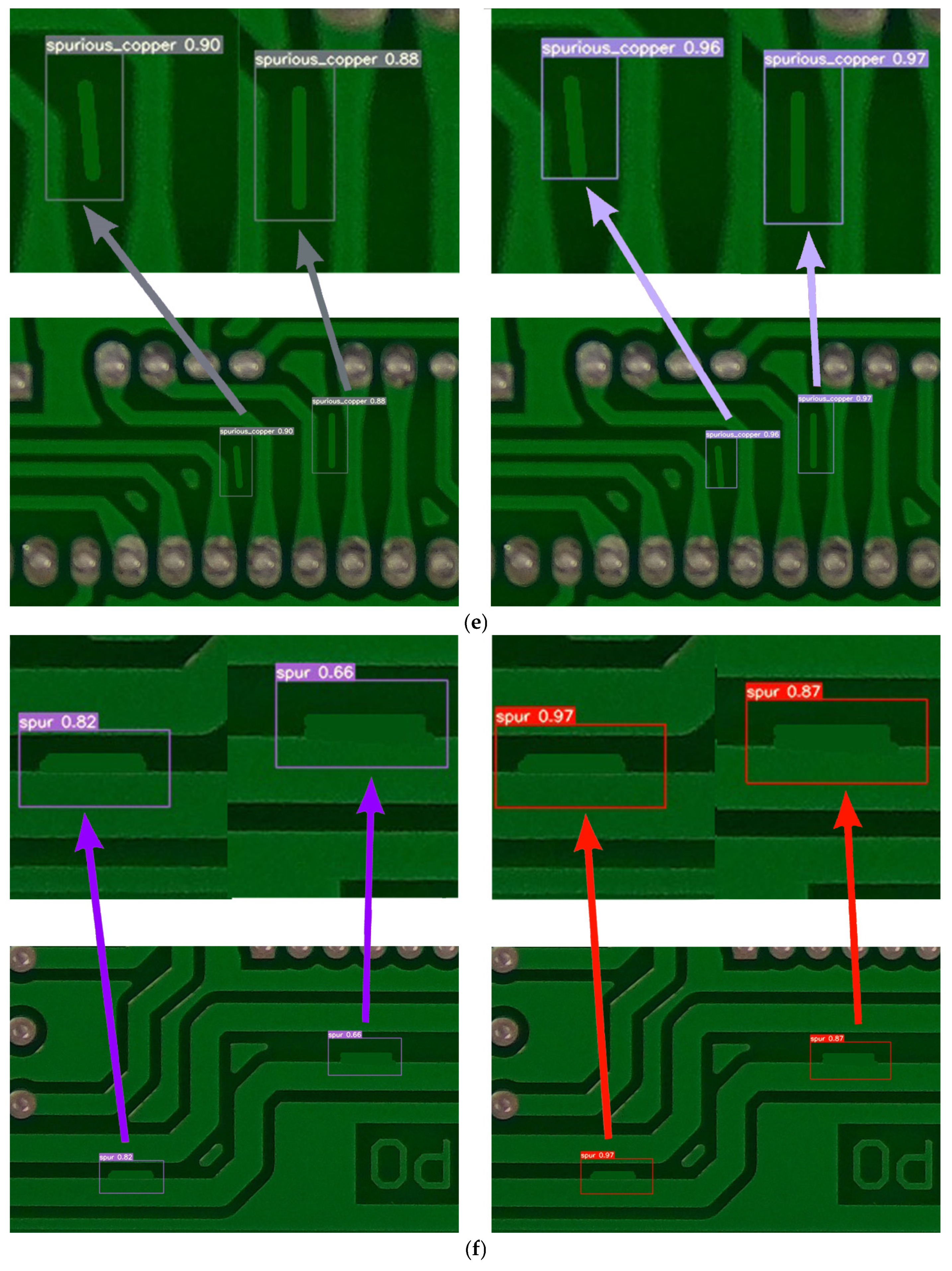
To more intuitively highlight the performance advantages of the algorithm, the YOLOv7 algorithm and SSHP-YOLO have been visualized and compared. The detection results are shown in Figure 5.
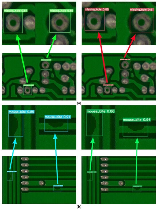

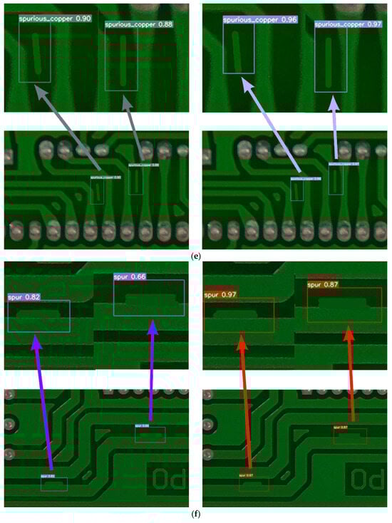
Figure 5.
Visual comparison results. (a) Visual comparison results: missing_hole. (b) Visual comparison results: mouse_bite. (c) Visual comparison results: open_circuit. (d) Visual comparison results: short. (e) Visual comparison results: spurious_copper. (f) Visual comparison results: spur.
The visual comparison results, as shown in Figure 5a–f, illustrate the detection performance of YOLOv7 and SSHP-YOLO on different PCB defects. Each figure consists of two images: the left image shows the detection results of YOLOv7, and the right image shows the results of SSHP-YOLO. The defect categories include (a) missing_hole, (b) mouse_bite, (c) open_circuit, (d) short, (e) spurious_copper, and (f) spur. The SSHP-YOLO model reduces false detections in open_circuit defect detection and missed detections in short defect detection, demonstrating its ability to correctly identify these defects. Furthermore, SSHP-YOLO achieves higher confidence levels in detecting six types of defects compared to YOLOv7, as shown in the experimental results. These findings validate the superior accuracy and reliability of the proposed algorithm.
4.7. Generalization Experiment Test
To verify the generality of the improvement algorithm in the field of defect detection, the NEU-DET public steel defect dataset was selected to train the YOLOv7 algorithm and SSHP-YOLO. The mAP was used as the evaluation indicator and the experimental results are presented in Table 6.
Table 6.
Generalization of the experimental results.
The mAP of the SSHP-YOLO model increased by 2.24% compared with YOLOv7, further demonstrating that the algorithm has strong generalization ability.
5. Conclusions
This paper tackles the challenges of PCB defect detection, including the complexity and high rates of false positives and negatives, by introducing an improved PCB defect detection algorithm, SSHP-YOLO, which builds upon enhancements to YOLOv7. First, the CBAM attention mechanism is incorporated into the ELAN-C module, thereby enhancing the model’s ability to focus on critical features of PCB defects. Subsequently, the SPPCSPC module is substituted with the ASPPCSPC module, which facilitates the capture of contextual information across different scales through dilated convolutions applied to the input PCB feature map at varying sampling rates. This modification substantially improves the detection accuracy and robustness of PCB defect identification. Furthermore, the SIoU loss function is employed instead of the traditional CIoU loss function, thereby improving the soft-matching relationship between the predicted bounding box and the ground truth. This substitution enhances the precision of bounding box predictions in target detection. Finally, ablation experiments are performed on the PKU-Market-PCB public dataset to assess the effectiveness of each improvement. The proposed model achieves a precision of 96.91%, a recall of 96.16%, and a mean average precision (mAP) of 97.80%. The superiority of the improved model is further validated through visual comparative analysis. To assess the model’s generalization ability, additional experiments are conducted on the NEU-DET public steel defect dataset, confirming the robustness and adaptability of the enhanced algorithm. This paper aims to tackle issues such as the low detection accuracy, frequent false positives and negatives, requirement for large training samples, and complexity of PCB defect detection. Future work will focus on reducing the model complexity and computational cost while maintaining the detection accuracy.
Author Contributions
Conceptualization, J.W. and L.M.; methodology, J.W.; software, L.M.; validation, L.M., Z.L. and Y.C.; formal analysis, J.W.; investigation, L.M.; resources, J.W.; data curation, L.M.; writing—original draft preparation, L.M.; writing—review and editing, J.W., Z.L., Y.C. and H.Z.; supervision, Y.C. All authors have read and agreed to the published version of the manuscript.
Funding
This research was funded by the Science and Technology Research Project of Henan Province, grant number 232102240097.
Data Availability Statement
The data presented in this study are available on request from the corresponding author.
Conflicts of Interest
The authors declare no conflicts of interest.
References
- Park, J.-H.; Kim, Y.-S.; Seo, H.; Cho, Y.-J. Analysis of Training Deep Learning Models for PCB Defect Detection. Sensors 2023, 23, 2766. [Google Scholar] [CrossRef] [PubMed]
- Pham, T.T.A.; Thoi, D.K.T.; Choi, H.; Park, S. Defect Detection in Printed Circuit Boards Using Semi-Supervised Learning. Sensors 2023, 23, 3246. [Google Scholar] [CrossRef] [PubMed]
- Yuan, Z.; Tang, X.; Ning, H.; Yang, Z. LW-YOLO: Lightweight Deep Learning Model for Fast and Precise Defect Detection in Printed Circuit Boards. Symmetry 2024, 16, 418. [Google Scholar] [CrossRef]
- Lv, S.; Ouyang, B.; Deng, Z.; Liang, T.; Jiang, S.; Zhang, K.; Chen, J.; Li, Z. A dataset for deep learning based detection of printed circuit board surface defect. Sci. Data 2024, 11, 811. [Google Scholar] [CrossRef]
- Chi, T.S.; Ab Wahab, M.N.; Mohamed, A.S.A.; Noor, M.H.M.; Kang, K.B.; Chuan, L.L.; Brigitte, L.W.J. Enhancing EfficientNet-YOLOv4 for Integrated Circuit Detection on Printed Circuit Board (PCB). IEEE Access 2024, 12, 25066–25078. [Google Scholar] [CrossRef]
- Klco, P.; Koniar, D.; Hargas, L.; Dimova, K.P.; Chnapko, M. Quality inspection of specific electronic boards by deep neural networks. Sci. Rep. 2023, 13, 20657. [Google Scholar] [CrossRef]
- Acciani, F.; Frasca, P.; Heijenk, G.; Stoorvogel, A.A. Achieving Robust Average Consensus Over Lossy Wireless Networks. IEEE Trans. Control Netw. Syst. 2019, 6, 127–137. [Google Scholar] [CrossRef]
- Annaby, M.H.; Fouda, Y.M.; Rushdi, M.A. Improved Normalized Cross-Correlation for Defect Detection in Printed-Circuit Boards. IEEE Trans. Semicond. Manuf. 2019, 32, 199–211. [Google Scholar] [CrossRef]
- Chen, X.; Wu, Y.; He, X.; Ming, W. A Comprehensive Review of Deep Learning-Based PCB Defect Detection. IEEE Access 2023, 11, 139017–139038. [Google Scholar] [CrossRef]
- Li, C.; Weng, X.; Li, Y.; Zhang, T. Multimodal Learning Engagement Assessment System: An Innovative Approach to Optimizing Learning Engagement. Int. J. Hum.–Comput. Interact. 2024, 24, 390–393. [Google Scholar] [CrossRef]
- Zhang, R.; Xu, L.; Yu, Z.; Shi, Y.; Mu, C.; Xu, M. Deep-irtarget: An automatic target detector in infrared imagery using dual-domain feature extraction and allocation. IEEE Trans. Multimed. 2021, 24, 1735–1749. [Google Scholar] [CrossRef]
- Li, C.-J.; Qu, Z.; Wang, S.-Y.; Bao, K.-H.; Wang, S.-Y. A Method of Defect Detection for Focal Hard Samples PCB Based on Extended FPN Model. IEEE Trans. Compon. Packag. Manuf. Technol. 2022, 12, 217–227. [Google Scholar] [CrossRef]
- Wang, Y.; Huang, J.; Dipu, M.S.K.; Zhao, H.; Gao, S.; Zhang, H.; Lv, P. YOLO-RLC: An advanced target-detection algorithm for surface defects of printed circuit boards based on YOLOv5. Comput. Mater. Contin. 2024, 80, 4973–4995. [Google Scholar] [CrossRef]
- Wang, Y.; Zhang, Y.; Liu, S.; Li, C. Enhancing Safety Perception in Autonomous Driving Systems Through 3D Object Detection and Neural Network Regression. In Proceedings of the 2024 2nd International Conference on Algorithm, Image Processing and Machine Vision (AIPMV), Zhenjiang, China, 16–18 August 2024; pp. 390–393. [Google Scholar]
- Song, X.; Wang, Y.; Li, C.; Song, L. WDC-YOLO: An improved YOLO model for small objects oriented printed circuit board defect detection. J. Electron. Imaging 2024, 33, 013051. [Google Scholar] [CrossRef]
- Redmon, J.; Divvala, S.; Girshick, R.; Farhadi, A. You only look once: Unified, real-time object detection. In Proceedings of the IEEE Conference on Computer Vision and Pattern Recognition, Las Vegas, NV, USA, 27–30 June 2016; pp. 779–788. [Google Scholar]
- Redmon, J.; Farhadi, A. YOLO9000: Better, faster, stronger. In Proceedings of the IEEE Conference on Computer Vision and Pattern Recognition, Honolulu, HI, USA, 21–26 July 2017; pp. 7263–7271. [Google Scholar]
- Redmon, J.; Farhadi, A. Yolov3: An incremental improvement. arXiv 2018, arXiv:1804.02767. [Google Scholar]
- Lin, T.Y.; Dollár, P.; Girshick, R.; He, K.; Hariharan, B.; Belongie, S. Feature pyramid networks for object detection. In Proceedings of the IEEE Conference on Computer Vision and Pattern Recognition, Honolulu, HI, USA, 21–26 July 2017; pp. 2117–2125. [Google Scholar]
- Bochkovskiy, A.; Wang, C.Y.; Liao, H.Y.M. Yolov4: Optimal speed and accuracy of object detection. arXiv 2020, arXiv:2004.10934. [Google Scholar]
- Ge, Z.; Liu, S.; Wang, F.; Li, Z.; Sun, J. Yolox: Exceeding Yolo series in 2021. arXiv 2021, arXiv:2107.08430. [Google Scholar]
- Li, C.; Li, L.; Jiang, H.; Weng, K.; Geng, Y.; Li, L.; Ke, Z.; Li, Q.; Cheng, M.; Nie, W.; et al. Yolov6: A single-stage object detection framework for industrial applications. arXiv 2022, arXiv:2209.02976. [Google Scholar]
- Wang, C.Y.; Bochkovskiy, A.; Liao, H.Y.M. YOLOv7: Trainable bag-of-freebies sets new state-of-the-art for real-time object detectors. arXiv 2022, arXiv:2207.02696. [Google Scholar]
- Du, B.; Wan, F.; Lei, G.; Xu, L.; Xu, C.; Xiong, Y. YOLO-MBBi: PCB Surface Defect Detection Method Based on Enhanced YOLOv5. Electronics 2023, 12, 2821. [Google Scholar] [CrossRef]
- Zhou, G.; Yu, L.; Su, Y.; Xu, B.; Zhou, G. Lightweight PCB defect detection algorithm based on MSD-YOLO. Clust. Comput.-J. Netw. Softw. Tools Appl. 2024, 27, 3559–3573. [Google Scholar] [CrossRef]
- Yuan, M.; Zhou, Y.; Ren, X.; Zhi, H.; Zhang, J.; Chen, H. YOLO-HMC: An Improved Method for PCB Surface Defect Detection. IEEE Trans. Instrum. Meas. 2024, 73, 2001611. [Google Scholar] [CrossRef]
- Xiao, G.; Hou, S.; Zhou, H. PCB defect detection algorithm based on CDI-YOLO. Sci. Rep. 2024, 14, 7351. [Google Scholar] [CrossRef] [PubMed]
- Luo, S.; Wan, F.; Lei, G.; Xu, L.; Ye, Z.; Liu, W.; Zhou, W.; Xu, C. EC-YOLO: Improved YOLOv7 Model for PCB Electronic Component Detection. Sensors 2024, 24, 4363. [Google Scholar] [CrossRef] [PubMed]
- Zhang, R.; Li, L.; Zhang, Q.; Zhang, J.; Xu, L.; Zhang, B.; Wang, B. Differential feature awareness network within antagonistic learning for infrared-visible object detection. IEEE Trans. Circuits Syst. Video Technol. 2023, 34, 6735–6748. [Google Scholar] [CrossRef]
- Zeng, Y.; Zhang, T.; He, W.; Zhang, Z. YOLOv7-UAV: An Unmanned Aerial Vehicle Image Object Detection Algorithm Based on Improved YOLOv7. Electronics 2023, 12, 3141. [Google Scholar] [CrossRef]
- Woo, S.; Park, J.; Lee, J.Y.; Kweon, I.S. CBAM: Convolutional block attention module. In Proceedings of the European Conference on Computer Vision (ECCV), Munich, Germany, 8–14 September 2018; pp. 3–19. [Google Scholar]
- Wei, G.; Wan, F.; Zhou, W.; Xu, C.; Ye, Z.; Liu, W.; Lei, G.; Xu, L. BFD-YOLO: A YOLOv7-Based Detection Method for Building Facade Defects. Electronics 2023, 12, 3612. [Google Scholar] [CrossRef]
- Yu, F.; Koltun, V. Multi-scale context aggregation by dilated convolutions. arXiv 2015, arXiv:1511.07122. [Google Scholar]
- Chen, H.-C.; Widodo, A.M.; Wisnujati, A.; Rahaman, M.; Lin, J.C.-W.; Chen, L.; Weng, C.-E. AlexNet Convolutional Neural Network for Disease Detection and Classification of Tomato Leaf. Electronics 2022, 11, 951. [Google Scholar] [CrossRef]
- Gevorgyan, Z. SIoU loss: More powerful learning for bounding box regression. arXiv 2022, arXiv:2205.12740. [Google Scholar]
- Liu, W.; Anguelov, D.; Erhan, D.; Szegedy, C.; Reed, S.; Fu, C.-Y.; Berg, A.C. SSD: Single Shot Multibox Detector. In Proceedings of the Computer Vision–ECCV 2016: 14th European Conference, Proceedings, Part I 14, Amsterdam, The Netherlands, 11–14 October 2016; pp. 21–37. [Google Scholar]
- Ren, S.; He, K.; Girshick, R.; Sun, J. Faster R-CNN: Towards real-time object detection with region proposal networks. IEEE Trans. Pattern Anal. Mach. Intell. 2015, 39, 1137–1149. [Google Scholar] [CrossRef] [PubMed]
- Duan, K.; Bai, S.; Xie, L.; Qi, H.; Huang, Q.; Tian, Q. Centernet: Keypoint triplets for object detection. In Proceedings of the IEEE/CVF International Conference on Computer Vision, Seoul, Republic of Korea, 27 October–2 November 2019; pp. 6569–6578. [Google Scholar]
- He, Q.; Xu, A.; Ye, Z.; Zhou, W.; Cai, T. Object Detection Based on Lightweight YOLOX for Autonomous Driving. Sensors 2023, 23, 7596. [Google Scholar] [CrossRef] [PubMed]
- Ding, R.; Dai, L.; Li, G.; Liu, H. TDD-net: A tiny defect detection network for printed circuit boards. CAAI Trans. Intell. Technol 2019, 4, 110–116. [Google Scholar] [CrossRef]
- Tang, J.; Liu, S.; Zhao, D.; Tang, L.; Zou, W.; Zheng, B. PCB-YOLO: An Improved Detection Algorithm of PCB Surface Defects Based on YOLOv5. Sustainability 2023, 15, 5963. [Google Scholar] [CrossRef]
- Deng, C.; Wang, M.; Liu, L.; Liu, Y.; Jiang, Y. Extended feature pyramid network for small object detection. IEEE Trans. Multimed. 2021, 24, 1968–1979. [Google Scholar] [CrossRef]
Disclaimer/Publisher’s Note: The statements, opinions and data contained in all publications are solely those of the individual author(s) and contributor(s) and not of MDPI and/or the editor(s). MDPI and/or the editor(s) disclaim responsibility for any injury to people or property resulting from any ideas, methods, instructions or products referred to in the content. |
© 2025 by the authors. Licensee MDPI, Basel, Switzerland. This article is an open access article distributed under the terms and conditions of the Creative Commons Attribution (CC BY) license (https://creativecommons.org/licenses/by/4.0/).