

Transistor Frequency-Response Analysis: Recursive Shunt-Circuit Transformations


Abstract
:1. Introduction: Frequency Response in Electronic Circuits
2. Proposed Frequency-Response Analysis
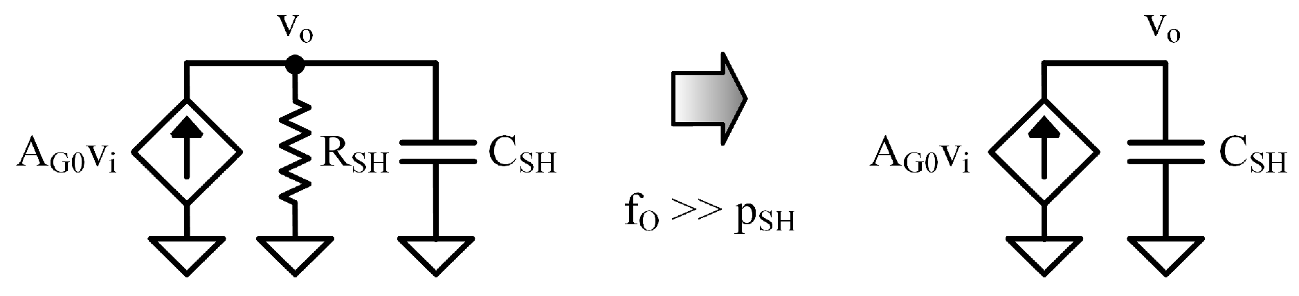
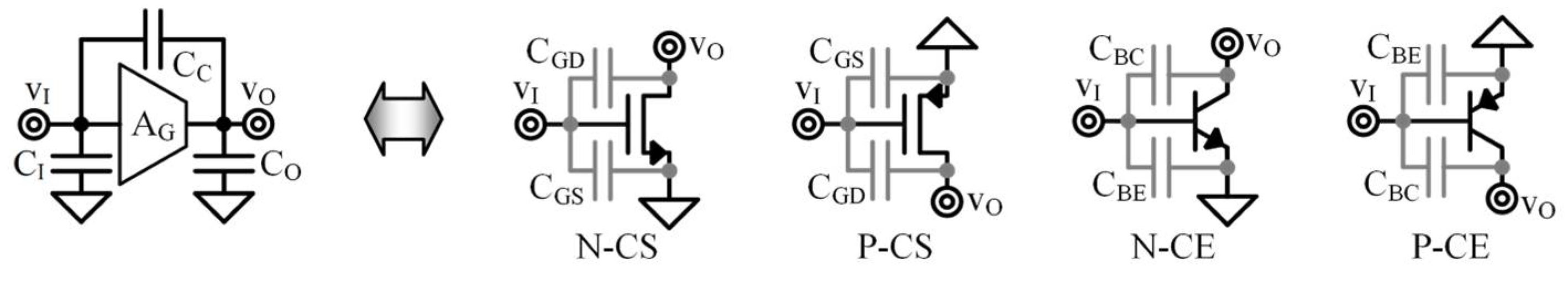
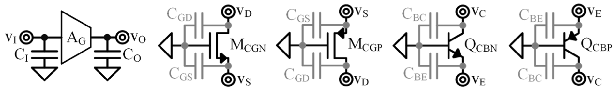
2.1. Shunt Circuits
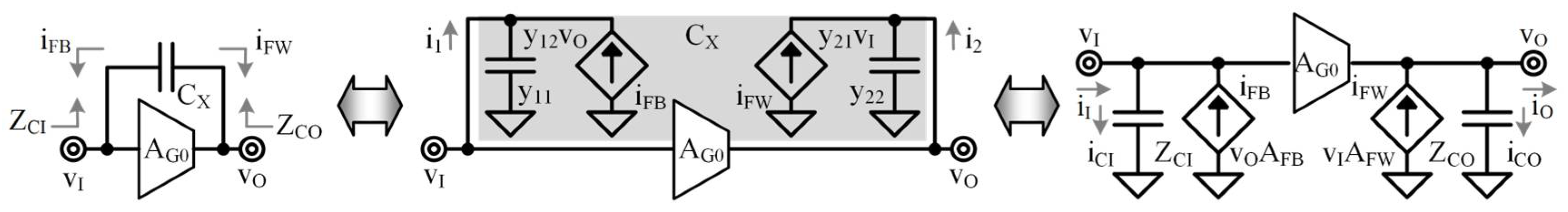
2.2. Feedback–Forward Split
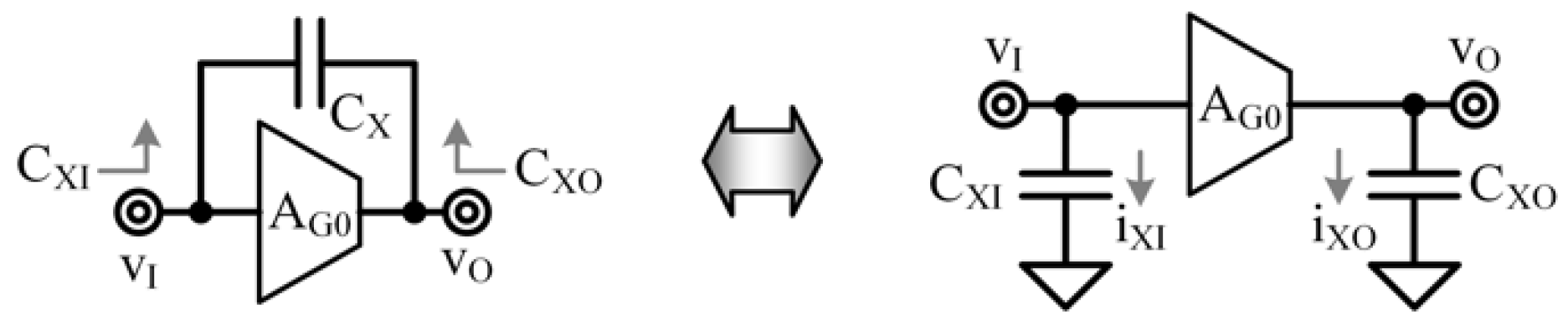
2.3. Cross-Amp Capacitance Split
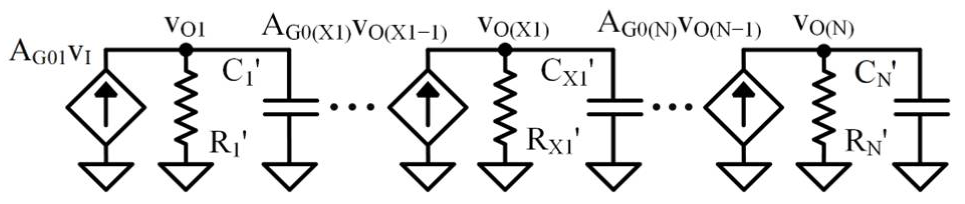
2.4. Recursive Shunt-Circuit Transformations
3. Common-Gate Stage
3.1. Low-Frequency Circuit for Common-Gate Stage
3.2. First-Pole Shunt Circuit for Common-Gate Stage
3.3. Second-Pole Shunt Circuit for Common-Gate Stage
3.4. Frequency Response for Common-Gate Stage
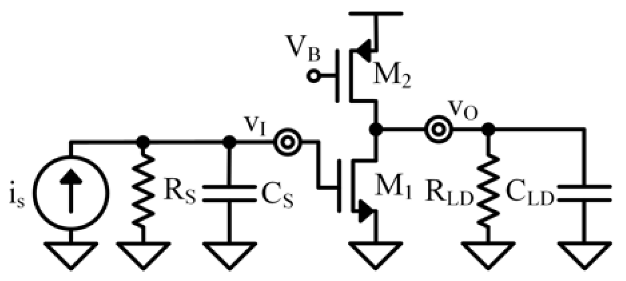
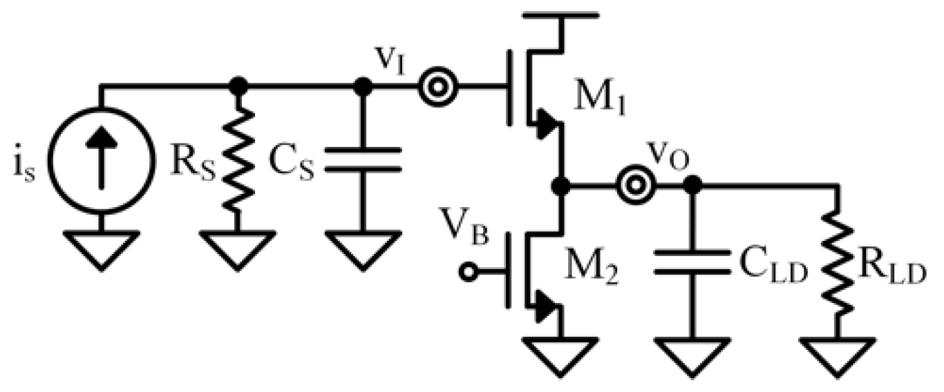
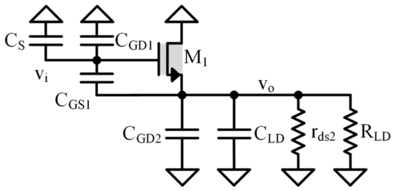
4. Common-Source Stage
4.1. Low-Frequency Circuit for Common-Source Stage
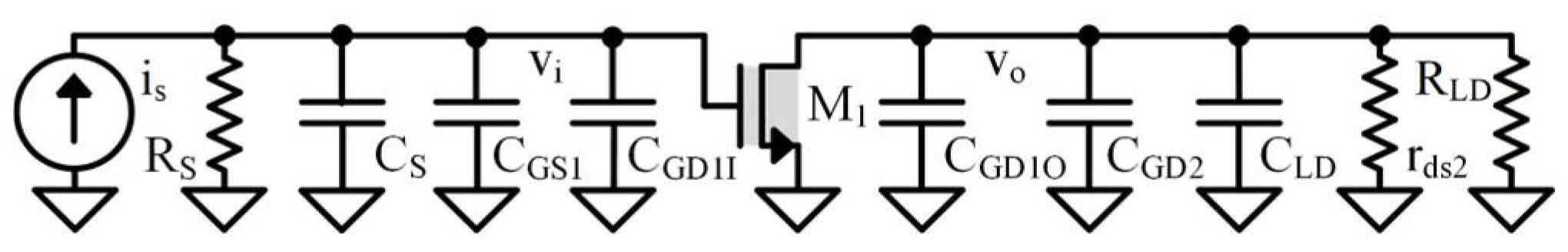
4.2. First-Pole Shunt Circuit for Common-Source Stage
4.3. Second-Pole Shunt Circuit for Common-Source Stage
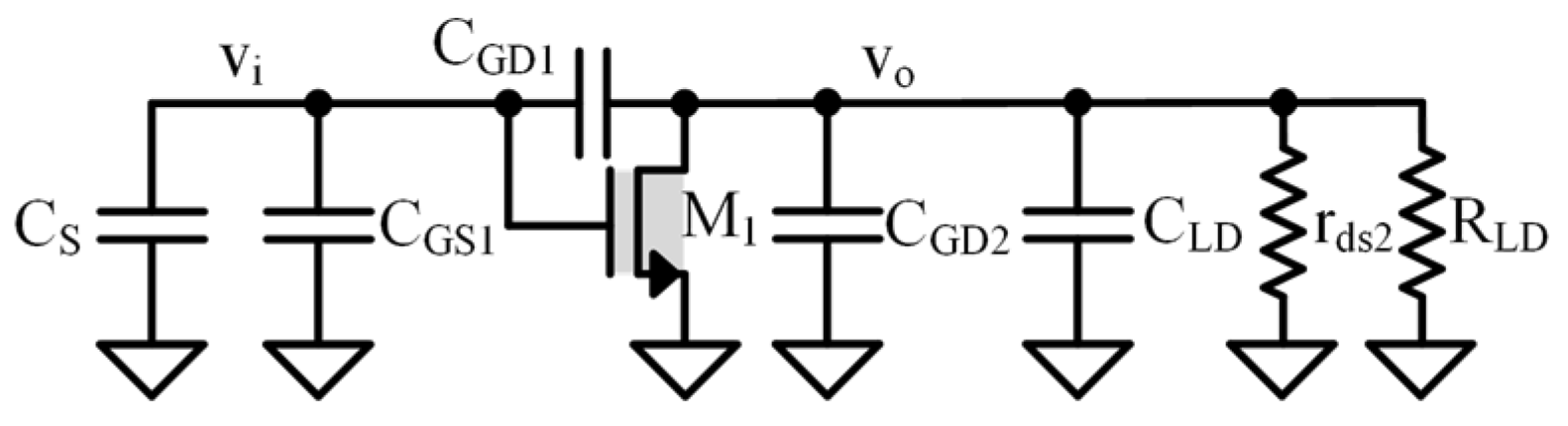
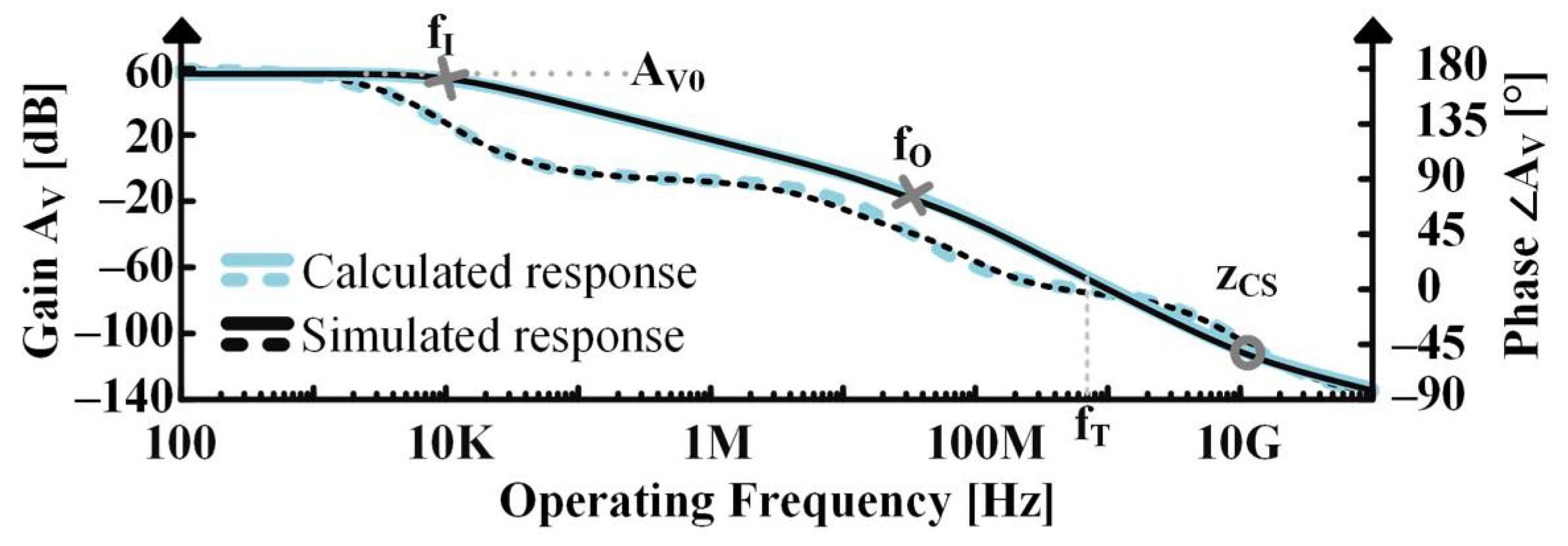
4.4. Frequency Response for Common-Source Stage
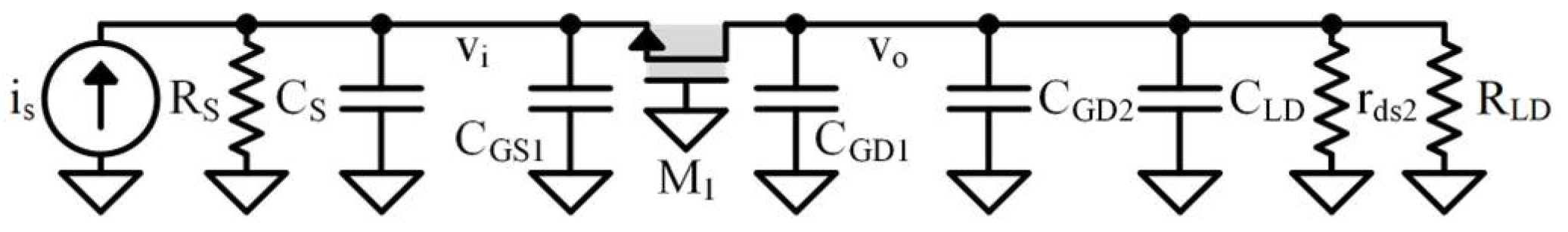
5. Common-Drain Stage
5.1. Low-Frequency Circuit for Common-Drain Stage
5.2. First-Pole Shunt Circuit for Common-Drain Stage
5.3. Second-Pole Shunt Circuit for Common-Drain Stage
5.4. Frequency Response for Common-Drain Stage
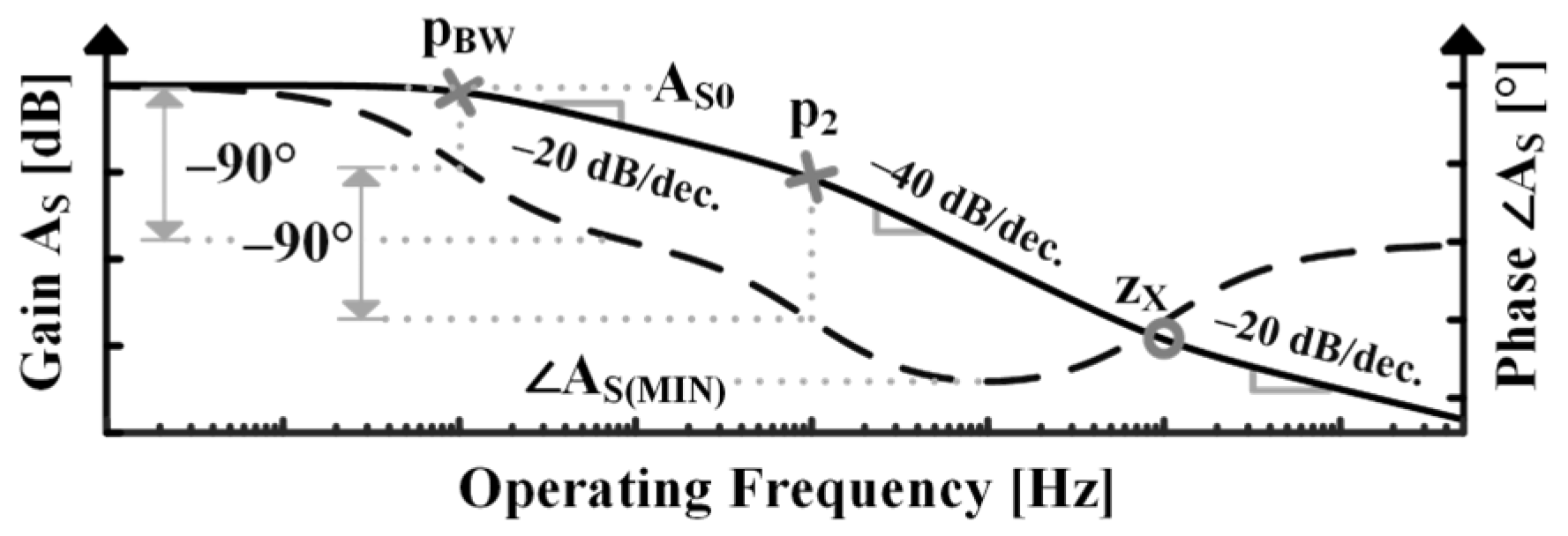
6. Clustered Poles
6.1. Coupled Poles
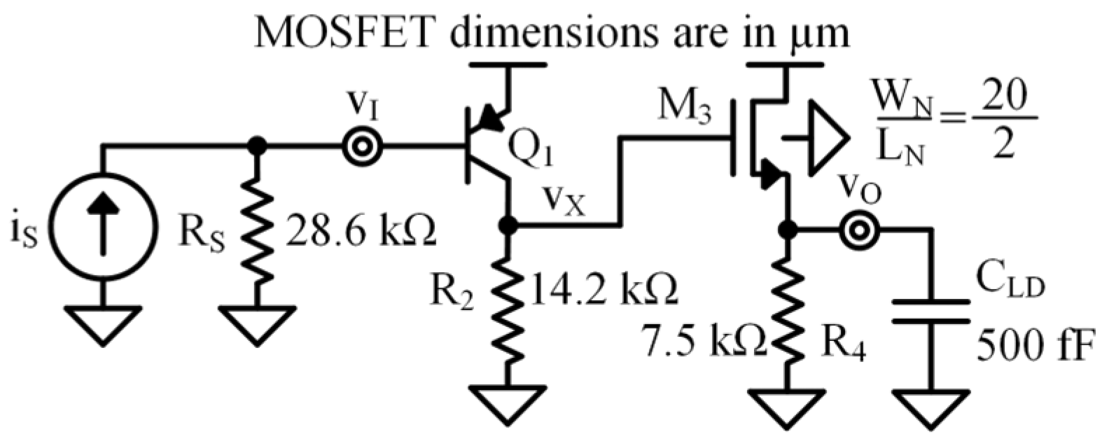
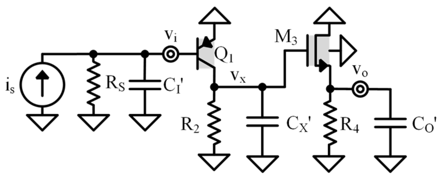
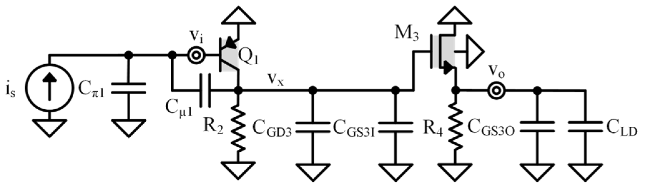
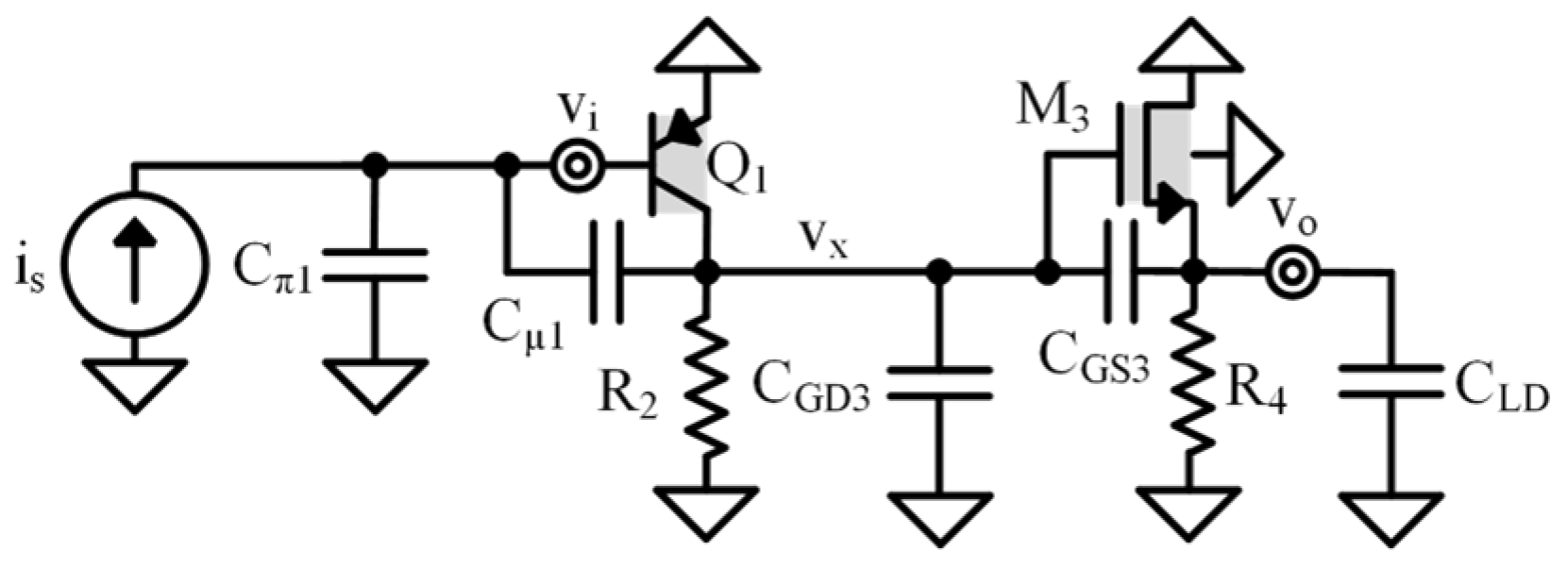
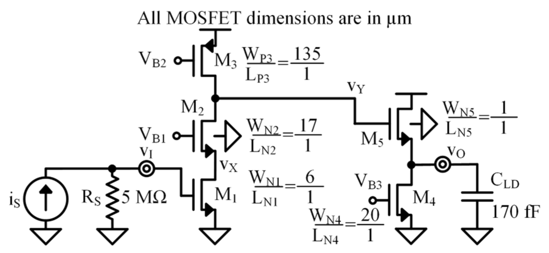
Common Emitter–Common Drain Design Example
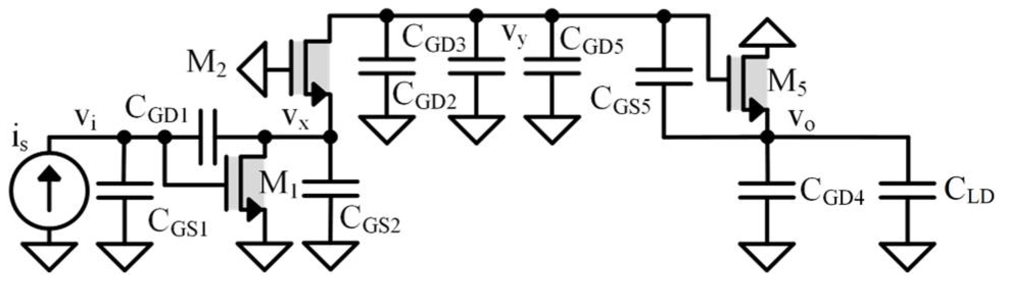
- Low-Frequency Common Emitter–Common Drain Circuit
- 2.
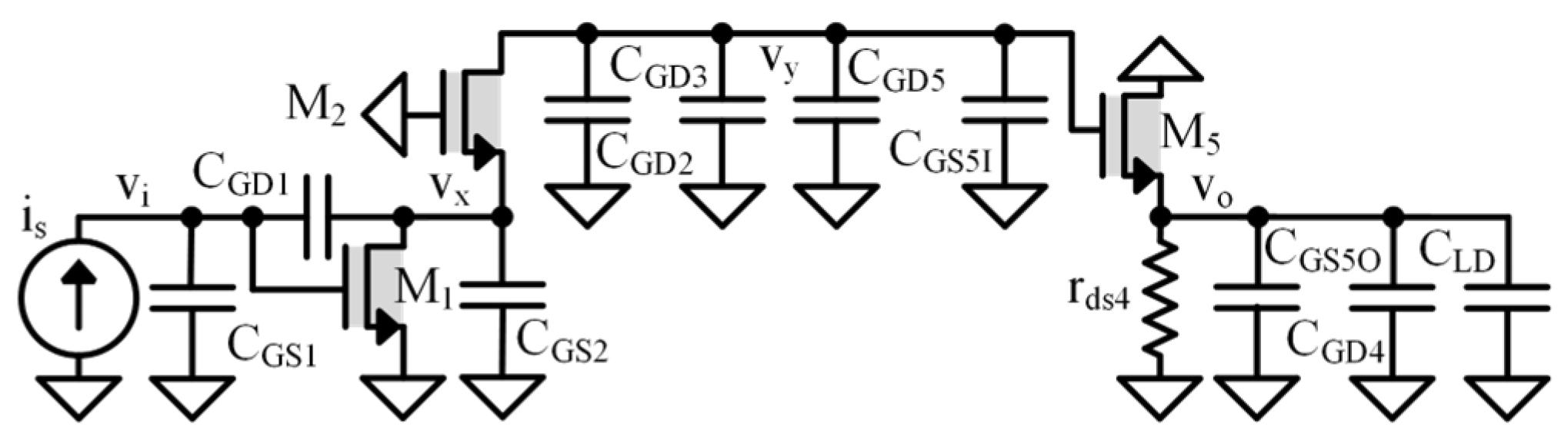
- First-Pole Common Emitter–Common Drain Shunt-Circuit
- 3.
- Second-Pole Common Emitter–Common Drain Shunt Circuit
- 4.
- Third-Pole Common Emitter–Common Drain Shunt Circuit
- 5.
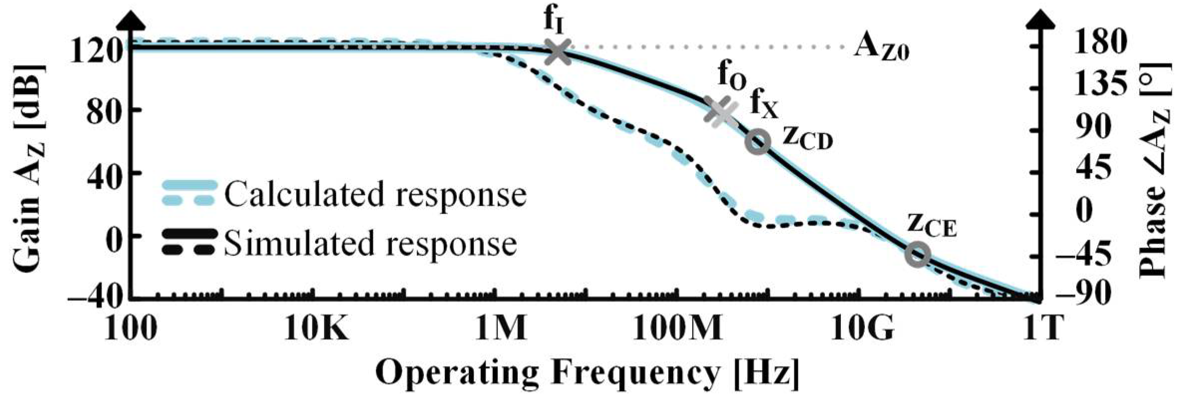
- Frequency Response for Common Emitter–Common Drain Circuit
6.2. Decoupled Poles
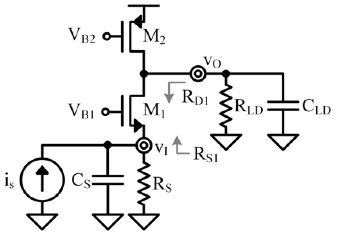
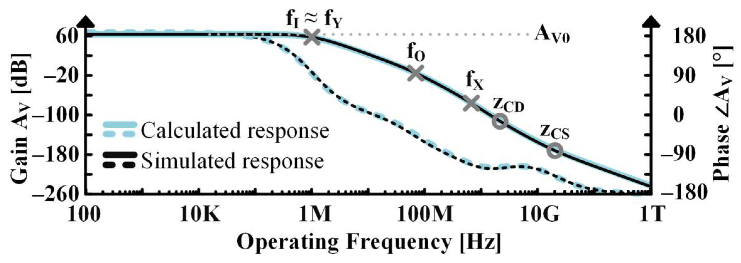
Common Source–Common Gate–Common Drain Design Example
- Low-Frequency Common Source–Common Gate–Common Drain Circuit
- 2.
- First-Pole Common Source–Common Gate–Common Drain Shunt Circuit
- 3.
- Second-Pole Common Source–Common Gate–Common Drain Shunt Circuit
- 4.
- Third-Pole Common Source–Common Gate–Common Drain Shunt Circuit
- 5.
- Fourth-Pole Common Source–Common Gate–Common Drain Shunt Circuit
- 6.
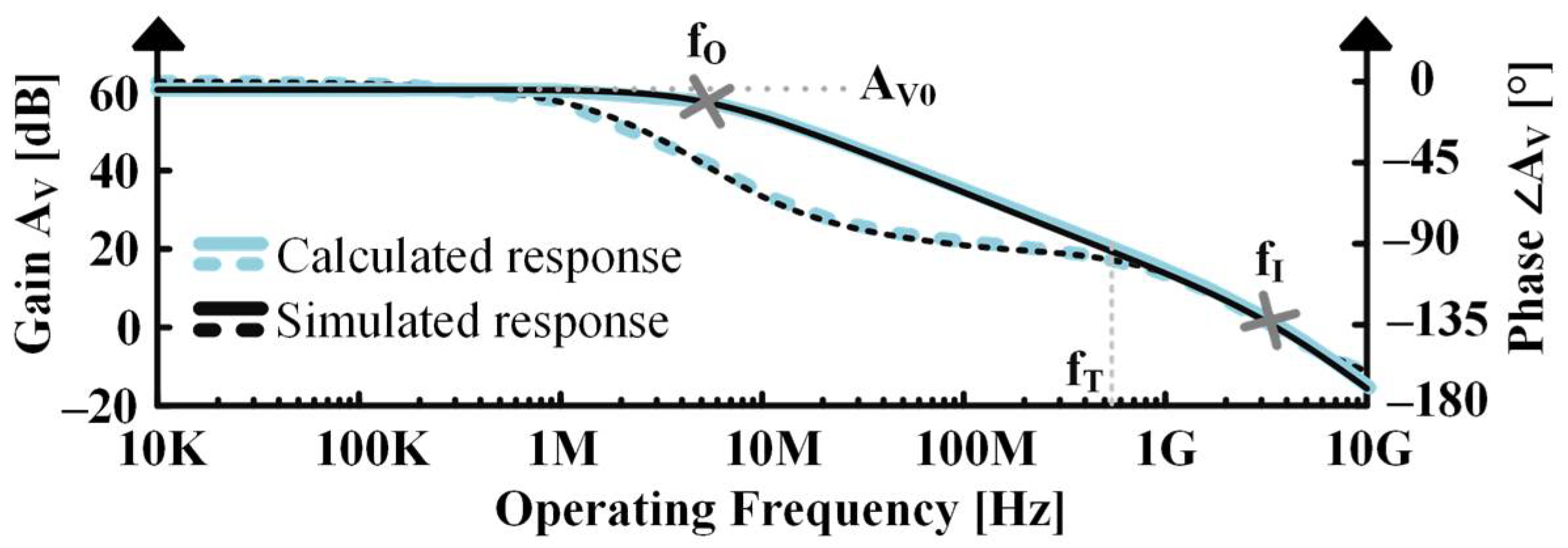
- Frequency Response for Common Source–Common Gate–Common Drain Circuit
7. Benefits for Design
7.1. Design Perspective
7.2. Direct Analysis
7.3. Graphical Analyses
7.4. Short-Circuit Approximation
7.5. Proposed Shunt-Circuit Approximation

| Stage | Pole Zero | Sim. | Direct | SoA | Error with Sim. | This Work | Error with Sim. |
|---|---|---|---|---|---|---|---|
| CG | pO | 5.0 MHz | 4.9 MHz | 4.9 MHz | −2.5% | 4.9 MHz | −2.5% |
| pI | 3.6 GHz | 3.6 GHz | 3.6 GHz | +1.9% | 3.6 GHz | +1.9% | |
| CS | pI | 10 kHz | 10 kHz | 10 kHz | −1.9% | 10 kHz | −1.9% |
| pO | 34 MHz | 35 MHz | 310 MHz | +810% | 34 MHz | −2.6% | |
| zCS | 11 GHz | 11 GHz | 11 GHz | +0.9% | 11 GHz | +0.9% | |
| CD | pI | 30 kHz | 30 kHz | 31 kHz | +3.3% | 31 kHz | +3.3% |
| pO | 3.1 MHz | 3.0 MHz | 58 MHz | +1800% | 3.0 MHz | −3.2% | |
| zCD | 280 MHz | 300 MHz | 300 MHz | +7.1% | 300 MHz | +7.1% |
| Stage | Pole Zero | Direct | SoA | This Work |
|---|---|---|---|---|
| CE-CD | pI | 4.9 MHz | 5.0 MHz | 5.0 MHz |
| pO | 230 MHz 1 | 450 MHz | 280 MHz | |
| pX | 370 MHz 1 | 950 MHz | 390 MHz | |
| zCD | 800 MHz | 800 MHz | 800 MHz | |
| zCE | 46 GHz | 46 GHz | 46 GHz | |
| CS-CG-CD | pI | 500 kHz 1 | 1.0 MHz | 1.0 MHz |
| pY | 2.0 MHz 1 | 17 MHz | 1.0 MHz | |
| pO | 60 MHz | 70 MHz | 70 MHz | |
| pX | 680 MHz | 730 MHz | 680 MHz | |
| zCD | 2 GHz | 2 GHz | 2 GHz | |
| zCD | 20 GHz | 20 GHz | 20 GHz |
8. Conclusions
Author Contributions
Funding
Data Availability Statement
Conflicts of Interest
References
- Rincón-Mora, G.A. Analog IC Design—An Intuitive Approach, 7th ed.; KDP: New York, NY, USA, 2019. [Google Scholar]
- Kamath, B.Y.; Meyer, R.G.; Gray, P.R. Relationship Between Frequency Response and Settling Time of Operational Amplifiers. IEEE J. Solid-State Circuits 1974, 9, 347–352. [Google Scholar] [CrossRef]
- Schubert, T.F. Heuristic Approach to the Development of Frequency Response Characteristics the Design of Feedback Amplifiers. In Technology-Based Re-Engineering Engineering Education, Proceedings of the Frontiers in Education FIE’96 26th Annual Conference, Salt Lake City, UT, USA, 6–9 November 1996; IEEE: New York, NY, USA; pp. 340–343. [CrossRef]
- Mazhari, B. On the Estimation of Frequency Response in Amplifiers Using Miller’s Theorem. IEEE Trans. Educ. 2005, 48, 559–561. [Google Scholar] [CrossRef]
- Alves, L.N.; Aguiar, R.L. Extending the Laplace Expansion Method to the Frequency Response Analysis of Active RLC Circuits. In Proceedings of the 10th IEEE International Conference on Electronics, Circuits and Systems, Sharjah, United Arab Emirates, 14–17 December 2003; Volume 3, pp. 1248–1251. [Google Scholar] [CrossRef]
- Potirakis, S.M.; Alexakis, G.E. An Accurate Calculation of Miller Effect on the Frequency Response and on the Input and Output Impedances of Feedback Amplifiers. IEEE Trans. Circuits Syst. II Express Briefs 2005, 52, 491–495. [Google Scholar] [CrossRef]
- Aminzadeh, H.; Grasso, A.D.; Palumbo, G. A Methodology to Derive a Symbolic Transfer Function for Multistage Amplifiers. IEEE Access 2022, 10, 14062–14075. [Google Scholar] [CrossRef]
- Cochrun, B.L.; Grabel, A. A Method for the Determination of the Transfer Function of Electronic Circuits. IEEE Trans. Circuit Theory 1973, 20, 16–20. [Google Scholar] [CrossRef]
- Abramovitz, A. A Practical Approach for Analysis of Input and Output Impedances of Feedback Amplifiers. IEEE Trans. Educ. 2009, 52, 169–176. [Google Scholar] [CrossRef]
- Fathi, A.; Khoei, A.; Mousazadeh, M. Generalized Method of Analog Circuit Characteristic Function Analysis. IEEE Trans. Circuits Syst. II Express Briefs 2019, 66, 172–176. [Google Scholar] [CrossRef]
- Razavi, B. Design of Analog CMOS Integrated Circuits, 2nd ed.; McGraw-Hill: New York, NY, USA, 2017; ISBN 9780072524932. [Google Scholar]
- Carusone, T.C.; Johns, D.A.; Martin, K.W. Analog Integrated Circuit Design, 2nd ed.; Wiley: Hoboken, NJ, USA, 2012. [Google Scholar]
- Jaeger, R.C.; Blalock, T.N. Microelectronic Circuit Design, 5th ed.; McGraw-Hill: New York, NY, USA, 2016. [Google Scholar]
- Miller, J.M. Dependence of the Input Impedance of a Three-Electrode Vacuum Tube upon the Load in the Plate Circuit. Sci. Pap. Bur. Stand. 1920, 15, 367–385. [Google Scholar] [CrossRef]
- Potirakis, S.; Alexakis, G.E. The Feedback Decomposition Theorem: The Evolution of Miller’s Theorem. Int. J. Electron. 1998, 85, 571–587. [Google Scholar] [CrossRef]
- Sedra, A.S.; Smith, K.C.; Carusone, T.C.; Gaudet, V. Microelectronic Circuits, 8th ed.; Oxford University Press: New York, NY, USA, 2020. [Google Scholar]
- Gray, P.R.; Hurst, P.J.; Lewis, S.H.; Meyer, R.G. Analysis and Design of Analog Integrated Circuits, 5th ed.; Wiley: Hoboken, NJ, USA, 2009. [Google Scholar]
- Huijsing, J.; Eschauzier, R. Frequency Compensation Techniques for Low-Power Operational Amplifiers, 1st ed.; Springer: New York, NY, USA, 1995. [Google Scholar]
- Huijsing, J. Operational Amplifiers—Theory and Design, 2nd ed.; Springer: Dordrecht, The Netherlands, 2011. [Google Scholar]
- Andreani, P.; Mattisson, S. Characteristic Polynomial and Zero Polynomial with the Cochrun–Grabel Method. Int. J. Circuit Theory Appl. 1998, 26, 287–292. [Google Scholar] [CrossRef]
- Andreani, P.; Mattisson, S. Extension of the Cochrun-Grabel Method to Allow for Mutual Inductances. IEEE Trans. Circuits Syst. I Fundam. Theory Appl. 1999, 46, 481–483. [Google Scholar] [CrossRef]
- Davis, A.M.; Moustakas, E.A. Analysis of Active RC Networks by Decomposition. IEEE Trans. Circuits Syst. 1980, 27, 417–419. [Google Scholar] [CrossRef]
- Fox, R.M.; Lee, S.G. Extension of the Open-Circuit Time-Constant Method to Allow for Transcapacitances. IEEE Trans. Circuits Syst. 1990, 37, 1167–1171. [Google Scholar] [CrossRef]
- Hajimiri, A. Generalized Time-and Transfer-Constant Circuit Analysis. IEEE Trans. Circuits Syst. I Regul. Pap. 2010, 57, 1105–1121. [Google Scholar] [CrossRef]
- Salvatori, S.; Conte, G.R. On the SCTC-OCTC Method for the Analysis and Design of Circuits. IEEE Trans. Educ. 2009, 52, 318–327. [Google Scholar] [CrossRef]
- Davis, A.M.; Moustakas, E.A. Decomposition Analysis of Active Networks. Int. J. Electron. 1979, 46, 449–456. [Google Scholar] [CrossRef]
- Thornton, R.D.; Searle, C.L.; Pederson, D.O.; Adler, R.B.; Angelo, E.J. Multistage Transistor Circuits; John Wiley & Sons: Hoboken, NJ, USA, 1965; ISBN 978-0471865056. [Google Scholar]
- Middlebrook, R.D. Null Double Injection and the Extra Element Theorem. IEEE Trans. Educ. 1989, 32, 167–180. [Google Scholar] [CrossRef]
- David Middlebrook, R.; Vorpérian, V.; Lindal, J. The N Extra Element Theorem. IEEE Trans. Circuits Syst. I Fundam. Theory Appl. 1998, 45, 919–935. [Google Scholar] [CrossRef]
- Gutierrez-Cortés, E.; Báez-López, D. On the Accurate Calculation of Miller Effect. In Proceedings of the 17th International Conference on Electronics, Communications and Computers—CONIELECOMP’07, Cholula, Mexico, 26–28 February 2007. [Google Scholar] [CrossRef]
- Ochoa, A. A Systematic Approach to the Analysis of General and Feedback Circuits and Systems Using Signal Flow Graphs and Drivingpoint Impedance. IEEE Trans. Circuits Syst. II Analog. Digit. Signal Process. 1998, 45, 187–195. [Google Scholar] [CrossRef]
- Tepwimonpetkun, S.; Pholpoke, B.; Wattanapanitch, W. Graphical Analysis and Design of Multistage Operational Amplifiers with Active Feedback Miller Compensation. Int. J. Circuit Theory Appl. 2016, 44, 562–583. [Google Scholar] [CrossRef]
- Vazzana, G.A.; Dario Grasso, A.; Pennisi, S. A Toolbox for the Symbolic Analysis and Simulation of Linear Analog Circuits. In Proceedings of the SMACD 2017—14th International Conference on Synthesis, Modeling, Analysis and Simulation Methods and Applications to Circuit Design, Giardini Naxos, Italy, 12–15 June 2017. [Google Scholar] [CrossRef]
- Fakhfakh, M. Design of Analog Circuits Through Symbolic Analysis; Bentham Science Publishers: Sharjah, United Arab Emirates, 2012. [Google Scholar] [CrossRef]
- Fontana, G.; Grasso, F.; Luchetta, A.; Manetti, S.; Piccirilli, M.C.; Reatti, A. A New Simulation Program for Analog Circuits Using Symbolic Analysis Techniques. In Proceedings of the 2015 International Conference on Synthesis, Modeling, Analysis and Simulation Methods and Applications to Circuit Design—SMACD 2015, Istanbul, Turkey, 7–9 September 2015. [Google Scholar] [CrossRef]
- Fernández, F.; Rodrígez-Vánquez, Á.; Huertas, J.L.; Gielen, G.G.E. Symbolic Analysis Techniques: Applications to Analog Design Automation; Wiley-IEEE Press: Hoboken, NJ, USA, 1998. [Google Scholar] [CrossRef]
- Allen, P.E.; Holberg, D.R. CMOS Analog Circuit Design, 3rd ed.; Oxford University Press: New York, NY, USA, 2012; ISBN 9780199765072. [Google Scholar]
- Palumbo, G.; Choma, J. An Overview of Analog Feedback Part I: Basic Theory. Analog Integr. Circuits Signal Process. 1998, 17, 175–194. [Google Scholar] [CrossRef]
- Zaidi, M.; Grout, I.; A’Ain, A.K. Evaluation of Compensation Techniques for CMOS Operational Amplifier Design. In Proceedings of the ICICDT 2018—International Conference on IC Design and Technology, Otranto, Italy, 4–6 June 2018; pp. 5–8. [Google Scholar] [CrossRef]
- Ochoa, A. On Stability in Linear Feedback Circuits. Midwest Symp. Circuits Syst. 1997, 1, 51–55. [Google Scholar] [CrossRef]
- Liu, X. Research on the Stability of Negative Feedback Circuit. Theor. Nat. Sci. 2023, 19, 193–199. [Google Scholar] [CrossRef]


| Parameters | ||
|---|---|---|
| ICS = 10 μA | WCS = 20 μm | L = 1 μm |
| ICD = 1 mA | WCD = 5 mm | LOL = 30 nm |
| ICG = 10 μA | WCG = 50 μm | KN′ = 200 μA/V 2 |
| COX″ = 7 fF/μm 2 | λN/P = 2% | KP′ = 40 μA/V 2 |
| RS(CS/CD) = 5 MΩ 1 | Ω | VDD = 5 V |
| fT(CS) = 470 MHz 2 | fT(CD) = 290 MHz 2 | fT(CG) = 280 MHz 2 |
| VTN0 = |VTP0| = 0.4 V | CJ0 = 50 fF | tf = 100 ps |
| β0 = 100 A/A | I2/4(CE-CD) = 200 μA | VA = 50 V |
| IS = 1fA | I3/4(CS-CG-CD) = 10 μA | γ = 600 mV |
Disclaimer/Publisher’s Note: The statements, opinions and data contained in all publications are solely those of the individual author(s) and contributor(s) and not of MDPI and/or the editor(s). MDPI and/or the editor(s) disclaim responsibility for any injury to people or property resulting from any ideas, methods, instructions or products referred to in the content. |
© 2025 by the authors. Licensee MDPI, Basel, Switzerland. This article is an open access article distributed under the terms and conditions of the Creative Commons Attribution (CC BY) license (https://creativecommons.org/licenses/by/4.0/).
Share and Cite
Manocha, P.; Rincón-Mora, G.A. Transistor Frequency-Response Analysis: Recursive Shunt-Circuit Transformations. Electronics 2025, 14, 296. https://doi.org/10.3390/electronics14020296
Manocha P, Rincón-Mora GA. Transistor Frequency-Response Analysis: Recursive Shunt-Circuit Transformations. Electronics. 2025; 14(2):296. https://doi.org/10.3390/electronics14020296
Chicago/Turabian StyleManocha, Pratyush, and Gabriel A. Rincón-Mora. 2025. "Transistor Frequency-Response Analysis: Recursive Shunt-Circuit Transformations" Electronics 14, no. 2: 296. https://doi.org/10.3390/electronics14020296
APA StyleManocha, P., & Rincón-Mora, G. A. (2025). Transistor Frequency-Response Analysis: Recursive Shunt-Circuit Transformations. Electronics, 14(2), 296. https://doi.org/10.3390/electronics14020296