Abstract
Model Predictive Control (MPC) is widely adopted for power electronics converters due to its ability to optimize system performance under dynamic constraints. However, its FPGA implementation remains challenging due to the complexity of Hardware Description Language (HDL) programming. This paper addresses this challenge by introducing a straightforward methodology that simplifies FPGA implementation using MATLAB R2022b Simulink HDL Coder. It is shown that HDL Coder yields favorable synthesis outcomes, both in terms of area and time, compared to hand-coded HDL. Notably, the proposed method achieves a significantly reduced sampling step for the MPC algorithm—down to 32 ns—marking a substantial improvement over state-of-the-art implementations. The Integrated Logic Analyzer (ILA) IP available in the Vivado tool is used during the HIL testing phase to facilitate the real-time observation and analysis required for debugging and confirming the FPGA-implemented controller performance. Additionally, this paper discusses the advantages of utilizing HDL Coder for simplifying the FPGA programming process in power electronics applications and addresses the design challenges encountered using this methodology.
1. Introduction
Model Predictive Control (MPC) is an advanced control strategy extensively used in power electronics converters, particularly in applications involving DC/AC converters [1,2]. This approach brings numerous advantages, including its simplicity in design, exceptional dynamic performance, capacity to address multiple control objectives, and simple incorporation of system constraints and nonlinearities. The fundamental parts in MPC algorithms are the prediction model, the cost function, and the optimization algorithm. MPC predicts the system’s future behavior within a specified time frame. Subsequently, by computing a cost function, it determines the optimal state to fulfill the controller’s objectives [3,4,5].
MPC controllers are divided into two main types: Continuous Control Set (CCS) and Finite Control Set (FCS) [6]. In CCS-MPC, a fixed frequency can be achieved through the use of a Pulse Width Modulation (PWM) block. This method involves calculating the control action, such as the modulating signal or duty ratio, and subsequently generating switching pulses. On the other hand, FCS-MPC typically does not aim for a fixed switching frequency. In each step of the control algorithm, FCS-MPCs select the optimal switching state without involving any modulator block. They focus on determining the optimal states from a limited set of switching options available in switching power converters [7]. This flexibility enables the adaptation of choosing the most suitable switching state in each step, resulting in variable switching frequencies rather than maintaining a fixed one [8]. Comparatively, CCS-MPC proves effective for addressing challenges with longer prediction horizons, while FCS-MPC is commonly utilized for applications with shorter prediction horizons in power electronics [9]. Particularly, the FCS-MPC approach has gained notable recognition for its emphasis on reducing the computational burden of the MPC algorithm by acknowledging that power converters can be modeled as discrete systems [10]. However, achieving small sampling steps remains a significant challenge for FCS-MPC implementations, which is addressed in this paper.
When considering hardware alternatives for the implementation of MPC algorithms in power electronics applications, several options emerge, such as Digital Signal Processors (DSPs), microcontrollers, and Field-Programmable Gate Arrays (FPGAs) [10,11]. The selection of the most suitable platform often depends on the specific application requirements or the programming knowledge of the designer. DSPs and microcontrollers, owing to their utilization of the widely familiar C language and ease of programming, are extensively employed in control applications [12]. However, FPGA stands out as a powerful alternative, particularly in high-frequency applications, due to its parallel processing capabilities, providing the flexibility to efficiently implement complex algorithms [11,13]. Despite the notable advantages of FPGAs, a significant challenge lies in the expertise required for Hardware Description Language (HDL) coding, such as Verilog or VHDL, which is commonly used in FPGA programming. Unlike the C language, which is more familiar to many power electronics engineers accustomed to DSP or microcontroller programming, HDL code demands a specific skill set that can pose a barrier for engineers transitioning to FPGA-based implementations.
Various FPGA programming methods are available, including hand-coded HDLs [14,15], High-Level Synthesis (HLS) [16,17], LabVIEW G language [18], and automatic HDL code generation [19]. Each method has distinct impacts on design efforts and synthesis/timing results [11], as thoroughly compared by Zamiri et al. [20]. Hand-coded HDL allows for precise hardware customization but demands significant FPGA expertise and time investment, often making it impractical for time-sensitive or industrial projects. HLS tools convert C/C++ into FPGA-compatible HDL codes, reducing design efforts but frequently yielding synthesis results inferior to hand-coded HDLs [20]. Similarly, LabVIEW G language, despite offering a user-friendly graphical programming environment, tends to result in high resource utilization [21], which limits its suitability for complex algorithms like MPC, where reaching small sampling steps is critical. In contrast, MATLAB’s HDL Coder and Xilinx System Generator (XSG) [22,23] provide automated HDL code generation, offering a balance between design simplicity and performance. While XSG is limited to Xilinx-AMD FPGA platforms, HDL Coder in MATLAB is versatile, supporting a wide range of FPGA vendors. Moreover, HDL Coder achieves comparable or superior synthesis results, as evidenced by this study, which demonstrates significantly reduced sampling steps and efficient resource utilization in MPC applications [24,25]. These attributes establish HDL Coder as a highly effective solution, overcoming the limitations of alternative methods and enabling accessible and optimized FPGA-based implementations.
A study by Saralegui et al. [19] demonstrated that utilizing MATLAB Simulink HDL Coder can produce synthesis results and timing performance very similar to hand-coded HDL when translating model equations into HDL design for applications such as a Hardware-In-the-Loop (HIL) model of a buck converter. However, the study does not delve into the detailed steps of the automatic translation process, nor the applicability of the method for MPC algorithms, which are more complex and difficult to design due to their control-flow structures. Similarly, Nasika et al. [26] used MATLAB Simulink HDL Coder for a converter firing control model in HVDC systems but did not quantify FPGA resource consumption or constraints, highlighting the need for further investigation into the hardware implications of automatic HDL generation, particularly in terms of resource efficiency and performance optimization. It is important to note that neither of these examples focused on MPC applications.
In contrast, Simulink HDL Coder has been successfully applied in few cases for the design of MPC algorithms. For instance, Singh et al. [27] explored a model-based design approach for implementing FCS-MPC for a three-phase voltage source inverter using MATLAB-Simulink. However, their work focused primarily on the simulation of the control system rather than offering a comprehensive guide to FPGA hardware implementation. Although the study highlighted the potential advantages of this approach for FPGA prototyping, it did not provide experimental results from an actual FPGA-based setup, leaving a gap in detailed procedural information necessary for FPGA implementation [27]. The same authors later implemented the MPC algorithm into an FPGA in [22]. However, the sampling step they achieved (50 s) is relatively large for most power electronics applications. Another relevant study presented by Siwakoti et al. [28] highlighted the use of MATLAB Simulink HDL Coder in the rapid prototyping of MPC controllers, enabling designers to model, simulate, and automatically generate VHDL code for FPGA implementation. It shows that the overall project development time is reduced by through HDL Coder design compared to manual coding. However, these examples do not delve into the detailed steps of the automatic translation process and the remaining challenges of using Simulink HDL Coder for MPC designs, such as reaching optimal synthesis/timing results.
Achieving smaller sampling steps in Finite FCS-MPC algorithms is crucial for enhancing control performance, particularly in reducing the Total Harmonic Distortion (THD) in load currents. Sankar et al. [29] demonstrate that smaller sampling intervals significantly lower THD, although this comes at the cost of increased resource usage. Their study reached a minimum sampling step of 1 s, which is among the smallest found in the state of the art for FCS-MPC controllers. Other studies have reported similar or larger sampling steps, such as 50 s in [22] and 1 s in [28].
While MATLAB Simulink HDL Coder has been introduced as an easy choice for initiating controller designs in FPGAs for power converters, there is a lack of detailed studies focusing on the actual design process. Most existing works mention its utility but do not delve into the step-by-step details of how to use it. This gap highlights the need for more comprehensive studies that guide users through the intricacies of MATLAB HDL Coder for power electronics designs. This paper introduces a step-by-step guide for the FPGA implementation of an MPC algorithm designed to regulate the injected current into the grid through an H-bridge converter. It begins with an in-depth analysis of the MPC controller and H-bridge converters, including the mathematical equations and discretized models essential for embedding such a control algorithm into an FPGA. The proposal involves breaking the complex MPC algorithm into general subblocks, which can be adapted to any new algorithm. This approach simplifies the design process, reducing the complexity that can often be challenging when implementing the algorithm in a graphical environment. Subsequently, the paper delves into the MPC controller design process in MATLAB HDL Coder, emphasizing the consideration of fixed-point numerical formats to enhance hardware resource optimization. After obtaining the VHDL codes from MATLAB tool, the design process in Vivado tool is presented to obtain the bitstream file needed for FPGA programming. For debugging internal digital signals within the FPGA, the Integrated Logic Analyzer (ILA) in Vivado is employed. The ILA enables designers to validate signal functionality and assess FPGA behavior in real time throughout the development process. Thus, this paper provides a comprehensive overview of the fast design and test process of MPC controllers in an FPGA by using MATLAB HDL Coder, highlighting the process from the starting point to the end, where the algorithm is tested using a real-time platform inside the FPGA.
This paper addresses the challenge of implementing Model Predictive Control (MPC) algorithms on FPGAs by introducing a systematic and accessible methodology using MATLAB Simulink HDL Coder. The key contributions of this work are as follows:
- Smaller sampling times: The proposed methodology achieves significantly smaller sampling steps compared to previous state-of-the-art Finite Control Set MPC (FCS-MPC) implementations. Experimental results demonstrate a sampling step of 500 ns to avoid high switching frequencies, with the capability to achieve steps as short as 32 ns, significantly surpassing state-of-the-art implementations.
- Efficient resource utilization: The study highlights new findings regarding the synthesis and execution of MPC algorithms on FPGAs, showing that HDL Coder enables synthesis results nearly identical to those achieved with hand-coded HDL. This is particularly important for resource-constrained and low-cost FPGA devices, ensuring efficient hardware resource utilization.
- Single clock-period execution: The methodology introduces a novel approach by executing the entire MPC algorithm within a single clock period, enabling fully parallel operation of the controller. This optimization ensures highly responsive and efficient real-time control, essential for applications requiring rapid switching, such as power electronics systems.
- Practical accessibility: By leveraging HDL Coder, the proposed methodology simplifies FPGA programming, making advanced MPC implementation accessible to engineers without deep expertise in hardware description languages. Additionally, comprehensive design details in the Vivado tool are provided, offering a complete workflow from pure simulation to a fully implemented controller in FPGA hardware.
- Unified HIL and Controller Integration: A key advancement is the integration of the HIL model of the converter with the MPC controller within the same FPGA. This approach resolves the clock mismatch issue reported in HIL tests, where the controller and the HIL model do not share the same clock, a limitation specific to HIL testing and not observed in real hardware setups. By unifying the HIL setup within the same FPGA, this method eliminates such synchronization challenges, simplifying the testing process. The integrated HIL setup also follows the same design methodology, facilitating efficient and accurate controller validation before deployment in real hardware systems.
The rest of this paper is organized as follows: Section 2 delves into the theoretical principles of MPC, presenting an overview and detailing the mathematical model of the grid-connected H-bridge, alongside the discrete-time model, cost function, and optimum state finder crucial for MPC’s implementation. Section 3 outlines the MPC implementation using MATLAB Simulink and HDL Coder, emphasizing the transition from a Simulink model to VHDL code suitable for FPGA programming. Section 4 elaborates on the FPGA implementation process, from importing the VHDL code into the Vivado tool to generating the bitstream file necessary for programming the FPGA, illustrating the practical aspects of bringing the designed MPC controller to life. Section 5 presents a thorough verification of the MPC algorithm through MATLAB simulations and HIL tests, demonstrating the efficacy and real-world applicability of the designed controller. Finally, the paper concludes with a comprehensive discussion in Section 6.
2. Model Predictive Control Overview
MPC is a control strategy that uses a dynamic model to predict the future behavior of a system based on current and upcoming inputs. It employs a predictive model, control objectives, and an optimization process to calculate optimal control actions, driving the system toward desired states within a specified timeframe. MPC controllers are divided in two main groups: FCS-MPC and CCS-MPC. When it comes to the control of switching power converters, FCS-MPC has several advantages over CCS-MPC. It limits control actions to a discrete set of feasible switching states, which aligns well with the finite and distinct states in power converters. This simplicity helps efficiently manage power switch states, striking a balance between control performance and computational ease. Hence, FCS-MPC is the selected control algorithm for this study.
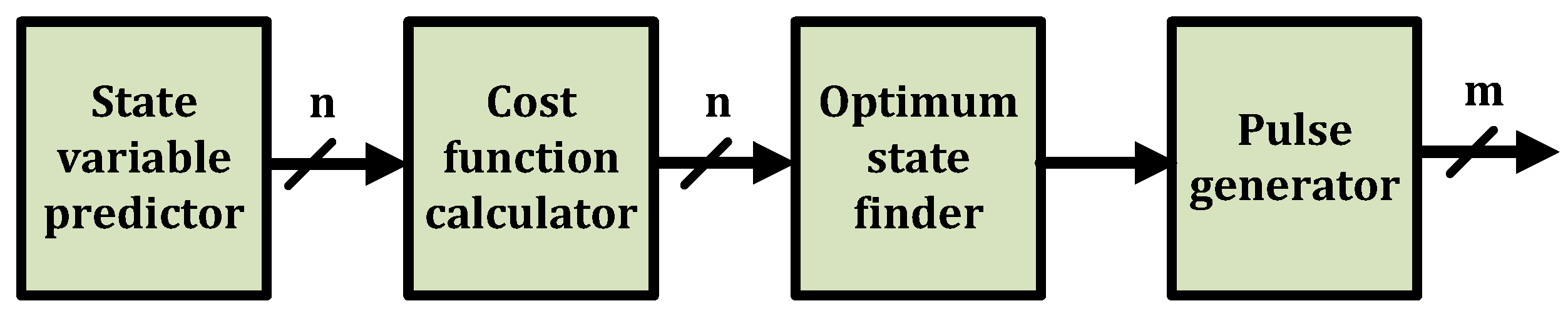
Figure 1 illustrates the fundamental stages of FCS-MPCs, where n denotes the number of states, and m represents the number of switches. The model computes all possible future behaviors (n possible values), selects the appropriate one considering control objectives that are involved in the Cost function calculator block, and then provides switching pulses for each switch (m switches in total) based on the optimum state for the next step.
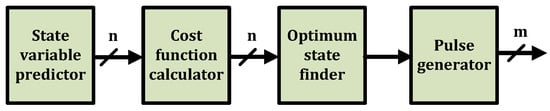
Figure 1.
Fundamental blocks of FCS-MPC controllers.
One of the main objectives of this study is to methodically demonstrate the step-by-step implementation of each block depicted in Figure 1 within an FPGA. Notably, to implement the MPC algorithm, particularly the State variable predictor block, mathematical equations of the controlled converter are required. Hence, an H-bridge converter, which is a simple and widely used power converter, is employed as the case study to highlight the FPGA implementation process.
2.1. Grid Connected H-Bridge Mathematical Model
Before formulating the MPC equations, it is crucial to comprehend the topology of an H-bridge converter connected to the grid. For this study, a single-phase H-bridge topology (Figure 2) is selected due to its simplicity, which allows the focus to remain on the workflow for prototyping the controller rather than being obscured by the additional complexity that might arise from more intricate converter designs. The topology includes two legs labeled as a and b, each with two switches, typically MOSFETs or IGBTs. The converter’s switching states are determined by the gating signals Sa and Sb, as defined in (1) and (2).
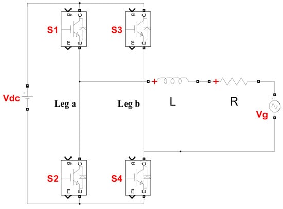
Figure 2.
Topology of a single-phase H-bridge converter.
Regarding possible combinations of and , the output voltage of the H-bridge inverter () is represented in three distinct forms summarized in Table 1, where is the input DC link voltage. The mathematical formulation of the converter output voltage is defined by (3):
where R is the resistance, L the inductance, the injected current to the grid, and is the grid voltage.

Table 1.
Possible voltage states of H-bridge.
2.2. Discrete-Time Model
To incorporate the converter model into a digital device, the differential equations of the converter must be discretized. Finite difference equations are employed for this purpose. The chosen discretization method is the forward Euler method, considered the most suitable for FPGA implementation due to its efficiency in minimizing computation time [30]. In the Euler discretization, the derivative term is replaced by the expression in (4), where denotes the sampling time.
Taking into account the possible switching states and the corresponding inverter output voltages, the inductor current can be described as depicted in (6). This equation will be implemented as the prediction step of the MPC algorithm and will need to be calculated for each state of the power converter.
2.3. Cost Function and Optimum State Finder
As demonstrated in Figure 1, once the prediction for each state variable is calculated, the subsequent step involves computing the cost function. In each MPC controller strategy, one or more control objectives are defined as reference variables. A reference is a desired or target value that the system aims to achieve for a particular variable or output. The MPC controller works to adjust the converter’s inputs over each sampling time to drive the actual outputs or state variables toward this reference. In this work, the reference is the desired inductor current intended to be injected into the grid. In the process, it optimizes a mathematical equation known as the cost function. In fact, the cost function serves as a criterion to quantify the error between the reference signals and the actual outputs at the next sampling instant (), aiming to identify the optimal state among the predicted ones from the previous instant (k). The cost function may vary based on the application and the defined control objective, which in this case study is defined by (7). The state that minimizes the cost function, indicating the closest match, () from (6), to the reference load current, (), is then chosen as the most suitable state for the application in the next sampling instant of the controller.
In (7), is the future reference current of the grid which is known in advance. For small sampling times, it can be assumed equal to , and is the predicted current for the next sampling interval. Consequently, the state that minimizes the cost function is identified as the optimal state. Then, based on optimized values, the MPC controller determines the corresponding switching actions for the power converter. This involves deciding the states (on or off) of all switches, as illustrated in Table 1, within the converter to achieve the desired output.
2.4. Adaptation for Off-Grid Applications
While this work focuses on grid-connected applications, the proposed algorithm can be adapted for off-grid standalone inverters with certain modifications. In standalone systems, the control algorithm must generate the voltage reference independently to maintain stable operation in the absence of grid synchronization. Equation (6) from the grid-connected scenario is modified to Equation (8), where represents the load connected to the inverter output. The algorithm determines the optimum state by solving Equation (9), where the reference voltage () corresponds to the voltage required by the load.
It is important to note that the rest of the equations required for MPC implementation, including optimum state finder and pulse generator blocks given in Figure 1, remain unchanged.
2.5. Adaptation for Three-Phase H-Bridge Inverter
The proposed methodology for FPGA implementation of MPC can be adapted to other power converter topologies, such as a three-phase H-bridge inverter shown in Figure 3, with minimal modifications to the predictive model and control framework. In this case, there is no need for d-q or - transformations, as the controller can directly operate in the abc frame by independently following the reference currents for each phase. The predictive model remains in the abc frame, and the control equations are extended to include all three phases. - and d-q transformations could also be used if preferred by the designer. In that case, the - or d-q currents would be calculated and used in the cost function instead of the abc currents.
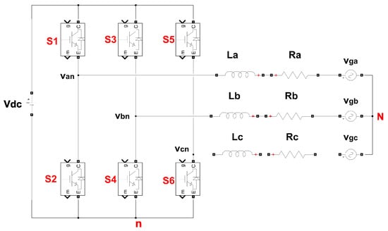
Figure 3.
Topology of a three-phase H-bridge inverter.
For a three-phase H-bridge inverter, the predictive model uses the following equations for each phase:
where is the grid voltage for phases a, b, and c, is the respective phase currents, and represents the voltages in each inverter leg. used in this formula is the voltage of the common node (N) in the grid side respecting the ground (n) that can be calculated as (11).
For the three-phase H-bridge topology, there are eight possible switching states, representing distinct combinations of switch positions for the three phases. The cost function evaluates each of these eight states to determine the optimal state that minimizes the tracking error between the predicted and reference currents. The cost function is modified to evaluate the tracking performance for all three phases simultaneously as given in (12). This ensures that the algorithm minimizes the current tracking error for each phase independently. Furthermore, because each reference current can be set separately, the controller is capable of handling unbalanced conditions, ensuring robust operation in scenarios where phase currents are not identical.
The modular design methodology described in this work can be directly applied with only minor adjustments to accommodate the three-phase predictive model and cost function. This approach is not limited to the three-phase H-bridge inverter; similar modifications can be applied to adapt the controller for other topologies. For instance, topologies such as three-level NPC converters, five-level cascaded H-bridge inverters, or multi-phase systems can follow the same principles, with the predictive model and cost function extended to account for the additional phases or voltage states.
3. MPC Implementation Alternatives in FPGAs
FPGA programming methodologies vary significantly in terms of design complexity, resource utilization, and performance optimization. Prominent approaches include hand-coded HDL, High-Level Synthesis (HLS), LabVIEW G language, and automatic HDL code generation tools such as MATLAB Simulink HDL Coder and Xilinx System Generator (XSG). This section explores the advantages of the proposed methodology using Simulink/HDL Coder by situating it within the broader landscape of FPGA programming methods.
3.1. FPGA Programming Alternatives
FPGA programming methodologies vary in complexity, performance, and accessibility, each offering unique advantages and disadvantages. Hand-coded HDL, High-Level Synthesis (HLS), LabVIEW G language, and automatic HDL code generation tools such as MATLAB Simulink HDL Coder and Xilinx System Generator (XSG) represent widely adopted approaches.
- Hand-Coded HDL: Hand-coded HDL provides the highest level of control and optimization, allowing designers to tailor FPGA implementations to meet precise performance requirements. Optimal results have been reported, such as integration steps as low as 17.7 ns [14]. However, this approach demands significant expertise in hardware description languages like Verilog or VHDL, as well as labor-intensive processes for design, debugging, and verification. These requirements make hand-coded HDL less accessible for designers without advanced FPGA knowledge, and increase development time.
- High-Level Synthesis (HLS): HLS tools aim to reduce design complexity by converting C/C++ code into FPGA-compatible HDL. While they simplify coding, the abstraction provided by HLS can obscure hardware details, leading to inefficiencies in resource utilization and timing performance without careful tuning [31]. Debugging is particularly complex, as it involves iterative refinement between the C/C++ and RTL levels. Additionally, the learning curve for mastering hardware-specific optimizations remains steep, and platform-specific constraints can limit portability, requiring redesign efforts for different FPGA targets. The quality of synthesized HDL also varies significantly, depending on algorithm complexity, tool capabilities, and designer expertise, which can make HLS less predictable for high-performance applications.
- LabVIEW G language offers a graphical interface, making it user-friendly for beginners. One of its main advantages is its robust debugging capabilities, which allow for effective signal analysis and validation within the National Instruments (NI) ecosystem. However, this strength comes at the expense of being tied to NI hardware, which is required not only for debugging but also for implementation. This dependency reduces flexibility for designers working with other FPGA platforms. Additionally, while LabVIEW simplifies design workflows, its high resource utilization can limit its suitability for resource-constrained applications like MPC controllers [21].
- Xilinx System Generator (XSG): XSG is a graphical tool specifically designed for Xilinx-AMD FPGAs, offering automated HDL code generation and better synthesis results for many applications compared with the LabVIEW G language alternative. However, according to [24], XSG produces worse synthesis results than MATLAB Simulink HDL Coder for MPC applications, making HDL Coder a preferable choice for such use cases. Additionally, XSG’s hardware-specific nature restricts its adaptability, as it is limited to Xilinx FPGAs. In contrast, HDL Coder is not only compatible with multiple FPGA vendors but also provides better synthesis results for MPC applications, making it a more versatile and efficient option.
- MATLAB Simulink HDL Coder: MATLAB Simulink HDL Coder was selected in this study due to its ability to effectively balance performance, accessibility, and adaptability. Unlike traditional hand-coded approaches, which require extensive FPGA expertise, HDL Coder automates the HDL code generation process, significantly reducing design complexity and development time. A critical factor in achieving a resource-optimized MPC model is the careful selection of signal formats, particularly in fixed-point arithmetic. Fixed-point formats allow efficient FPGA resource utilization by minimizing the hardware overhead associated with operations like multiplication and division. MATLAB Simulink HDL Coder excels in this regard, as it enables designers to seamlessly simulate the suitability of different signal formats within the Simulink environment before generating the HDL code. This simulation-based approach is far easier than alternatives like hand-coded HDL, where manual adjustments are required at the RTL level, or HLS tools, which involve iterative debugging between abstract C/C++ models and synthesized HDL. In contrast, HDL Coder provides an intuitive, graphical interface where designers can directly verify numerical precision and dynamic range, ensuring optimal signal representation without extensive trial-and-error. Unlike hardware-specific tools like XSG or LabVIEW, HDL Coder supports a wide range of FPGA families, including Xilinx’s Zynq and Kintex series, Intel’s Cyclone and Stratix series, and Lattice’s MachXO and iCE40 series, enhancing its versatility and portability across different hardware environments. Additionally, its seamless integration with MATLAB/Simulink enables iterative refinements within a unified environment, greatly simplifying the workflow. These attributes make it an ideal choice for implementing the MPC algorithms explored in this study.
3.2. MATLAB Simulink/HDL Coder
Instead of using hand-coded HDL, MATLAB Simulink HDL Coder is employed in this work for automatic HDL code generation. Hand-coding HDL complicates the initial phase of closed-loop verification, as HDL simulators cannot directly run power electronics schematics. In contrast, designing in MATLAB allows for the simultaneous simulation of control algorithms and power electronics schematics. Furthermore, the multi-stage design and verification methodology introduced in this paper for MPCs within a single FPGA enables stage-by-stage verification resulting in development time reduction. The use of Simulink/HDL Coder facilitates simulation of the MPC controller in conjunction with the converter designed in Simscape. This integration allows for comprehensive verification of the control algorithm without the need for external HIL equipments.
This section provides a clear, step-by-step guide for the straightforward FPGA implementation of MPC controllers, ranging from the simulation of the controller in MATLAB Simulink (Simscape) to the complete implementation of the system inside the FPGA. The first key step towards FPGA implementation involves obtaining the necessary HDL code for the system. This section specifically focuses on designing an MPC controller for a single-phase H-bridge, utilizing MATLAB Simulink HDL Coder to extract the required VHDL code for FPGA implementation. HDL Coder simplifies the creation of synthesizable HDL code by utilizing predefined graphical blocks and components from its library. Notably, this method eliminates the requirement for expertise in hand-coded HDL, making it accessible and user-friendly for power electronics engineers who may not possess extensive knowledge in this domain.
Simulink HDL Coder offers significant advantages in simplifying FPGA programming; however, it presents challenges when implementing control-flow operations common in software-based control algorithms. Structures like conditional statements (if-else), loops (for, while), and jumps can be more complex to manage in HDL Coder due to its emphasis on parallel arithmetic operations. For instance, an if-else statement requires the use of a multiplexer, while a for-loop necessitates loop unrolling, replicating the loop body for each iteration. These limitations can complicate designs that rely heavily on software-like control logic. In contrast, arithmetic operations integral to MPC algorithms, such as cost function calculations and predictions, align well with the HDL Coder environment. To address the specific demands of FCS-MPC in HDL Coder, this paper proposes a modular design approach using subblocks. By structuring the MPC control logic into independent sub-blocks within a single clock cycle, this method not only simplifies the design process and minimizes the complexity of control-flow structures but also ensures scalability. The modular nature of the approach allows it to be adapted easily to more complex control algorithms or extended to handle additional functionalities without significant redesign, making it versatile for a range of applications.
Figure 4 presents the full schematic of the MPC design in HDL Coder, similar to the structure seen in Figure 1. This schematic is representative of any FCS-MPC controller, as the fundamental structure remains the same across different applications. Each subblock in this schematic corresponds to specific equations that are calculated in parallel, contributing to the reduction in sampling step. Although the subblocks perform their operations concurrently, the overall execution of the blocks, highlighting the information flow, is sequential. Importantly, all of these calculations are executed within a single clock period, with the clock period needing to be greater than the cumulative delay introduced by each subblock. This ensures that the entire MPC algorithm can be computed within a single clock cycle.
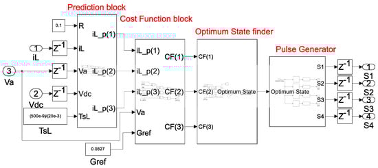
Figure 4.
Modular blocks for the implementation of FCS-MPC designs in HDL Coder, highlighting the single clock cycle execution and information flow to simplify control logic and enhance FPGA efficiency.
As previously discussed, this case study delves into MPC for controlling the inductor current, where and . In the prediction phase, the calculation of three future inductor current values (, where , 2, and 3) is derived from the measured inductor current () and grid voltage (). Figure 5 visually represents the formulation of (6) within the prediction block using HDL Coder library blocks. This schematic is the direct implementation of (6) and it becomes evident that this graphical method can be easily used without any prior knowledge of HDLs. The use of product and adder blocks from the HDL Coder library is notable for expressing mathematical operations involving multiplication and addition. It is crucial to highlight that parameters such as resistor value (R), input voltage source (), and inductor inductance (L) can vary in different applications. Therefore, the model must be designed for a specific example and cannot be universally applied to the same converter with different parameters. Additionally, due to limited number of FPGA resources, and taking into account that divisions often involve a larger and more complex circuit, sampling time () and the inductor inductance (L) are merged into a single parameter as to avoid the division of inside the FPGA.
Figure 5.
The inductor current predictor block in HDL Coder.
Upon calculating all predicted currents () for each state, the cost function checks how much they differ from the reference current (). Choosing an appropriate cost function is important for optimizing the controller’s performance and determining the most suitable state for future control actions. Figure 6 shows the representation of (7) using the HDL Coder library. Typically, in grid-connected systems, a higher-level controller decides the power to be injected into the grid. However, in this study, an electrical conductance () is introduced to adjust the injected power level. Indeed, is employed to represent the reference current (). Given that division operations in FPGAs demand more hardware resources than addition or multiplication, the reference current is determined by instead of to avoid the need for division. is directly measured grid voltage in this simple example but would be generated by a PLL (Phase Locked Loop) block in an industrial application.
Figure 6.
The cost function block in HDL Coder.
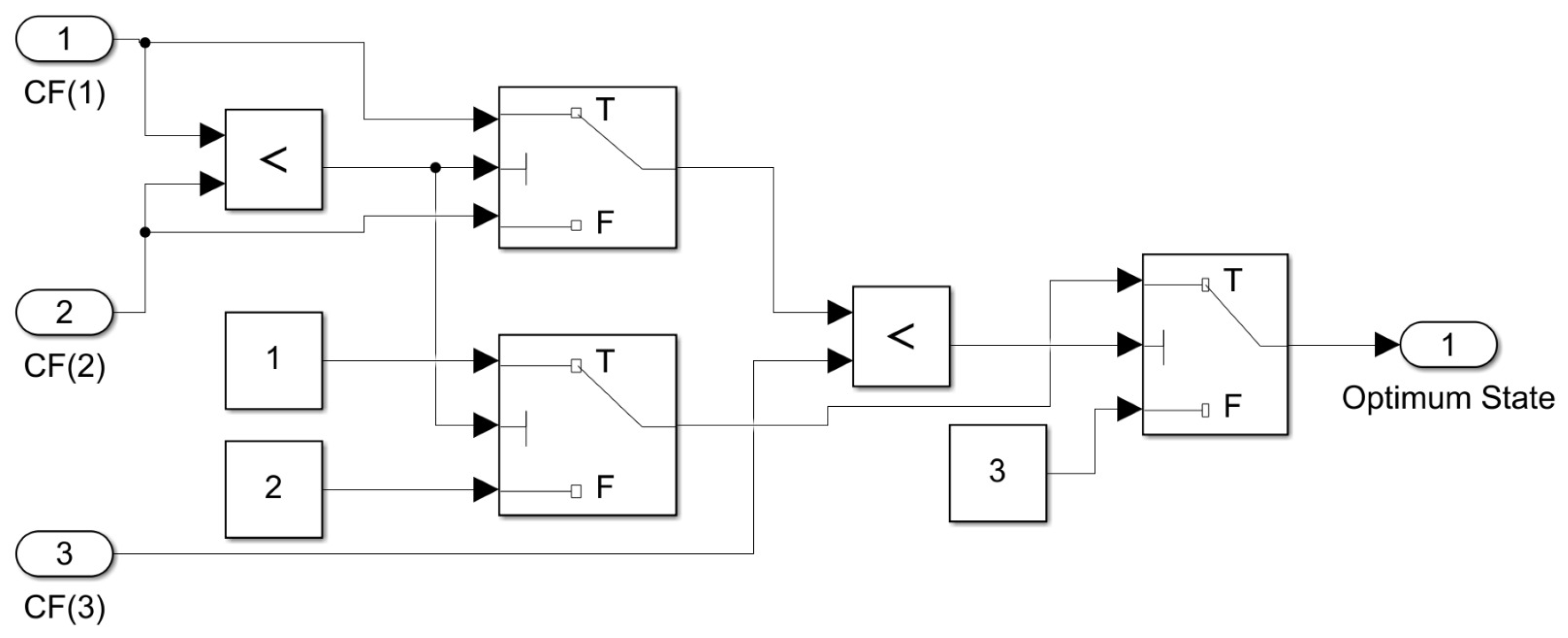
The optimum state is determined by analyzing the cost function values () derived from the previous step for each of the three states. The state exhibiting the minimum cost function value will be selected as the optimal, indicating minimal difference between the reference current () and the actual inductor current (). The proposed design of the optimum state finder block is illustrated in Figure 7. According to the result of each comparison among the values of the cost function, the number of the optimal state is directed to the output of this block.

Figure 7.
The optimum state finder block in HDL Coder.
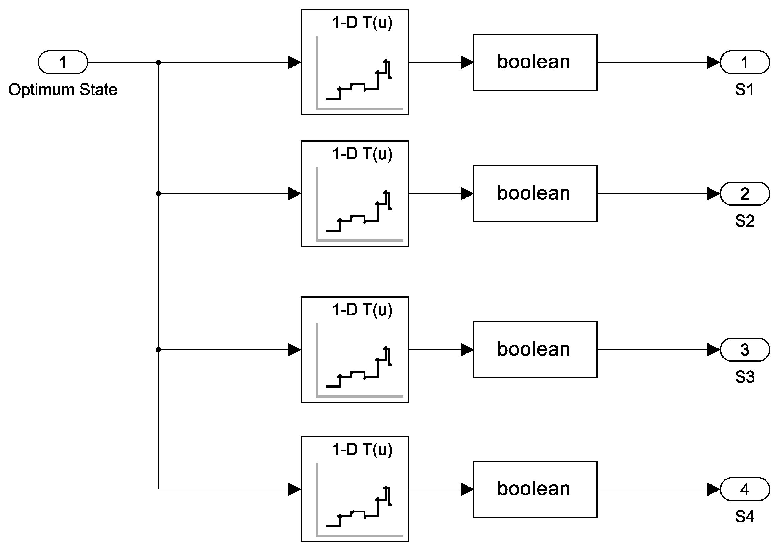
Ultimately, after identifying the optimal state, the controller generates pulses to align the system’s behavior with the desired objectives. The pulse generator block, depicted in Figure 8, takes the optimal state as input and utilizes various lookup tables to produce pulses. These pulses represent the selected switching state and serve as outputs of the controller.
Figure 8.
The pulse generator block in HDL Coder.
At this step, the MPC controller, designed using Simulink HDL Coder blocks, is ready for VHDL code generation. Initially, all signals are in double format (floating-point), which offers a large dynamic range and high precision. This format is ideal for verifying the MPC algorithm, as there are no concerns about signal resolution or range. However, before proceeding to VHDL generation, all parameters and signals must be converted to fixed-point format for several reasons. Firstly, fixed-point arithmetic operations demand fewer hardware resources compared to floating-point operations, making them more suitable for FPGA implementations. Secondly, FPGA architectures are inherently optimized for fixed-point computations, as they perform these operations with lower latency, which is critical in high-frequency applications. Additionally, fixed-point format allows for a more efficient and straightforward interface between the controller and the converter, given the limited signal width in DAC/ADC systems.
In this phase, the designer must carefully select the appropriate numerical format for each signal, balancing accuracy, precision, and resource usage. Specifically, the number of integer bits is chosen based on the expected range of values to prevent overflow, while the number of fractional bits is selected to ensure sufficient resolution for the application. The correct bit-width ensures efficient FPGA operation, preventing issues such as saturation or inadequate resolution. For instance, critical signals like the cost function and predicted current must be accurate enough to avoid erroneous decision-making by the controller, while still using minimal hardware resources. Furthermore, this process must take into account the area constraints of the FPGA, as well as the frequency targets that need to be met.
The fixed-point numerical format involves defining parameters such as the number of integer bits, fractional bits, and one sign bit. The integer bits represent the signal range, while the fractional bits determine its resolution. This data type in HDL Coder is defined as fixdt(S, T, F), where S represents the sign bit (1 for signed signals and 0 for unsigned ones), T represents the total number of bits (integer, fractional, and the sign bit), and F represents the number of fractional bits. For instance, considering the grid voltage as in this example, the numerical format is represented as fixdt(1, 16, 6). This indicates that the signal can range from to with a resolution of , as it is a signed signal with nine integer bits and six fractional bits.
In this paper, all signals are proposed to be assigned a 32-bit width, except for those involved in multiplications. The fixed-point format for multiplication, performed by DSP blocks in the FPGA, should adapt to the width of the inputs of the multipliers of the specific device to be used, as proposed by Zamiri et al. [32]. Since a Zynq-7000 device will be used in this example, the inputs of the multipliers have been limited to 18 and 25 bits (one input of 18 bits and the other one of 25 bits). This is to avoid using more DSP blocks and to optimize hardware resources in the FPGA setup. In this way, the synthesis results are optimal, as will be shown in the next section. After adjusting all signal formats accordingly, the controller performance must be verified again to ensure the accuracy of the final design in HDL Coder. Once the controller is successfully verified, the VHDL codes can be generated by selecting the main MPC block in Simulink, navigating to the APPS tab, and clicking on Generate HDL Code. This process facilitates the translation of the MPC model into VHDL code for FPGA implementation.
4. FPGA Implementation
In the previous section, it was explained how to design and extract the VHDL code for the MPC controller. This code can be simply added to the Vivado tool, facilitating the generation of bitstream file (.bit file) necessary for programming FPGAs. To generate the .bit file in the Vivado tool from the VHDL code obtained through HDL Coder, a series of structured steps are followed. First, the VHDL code, representing the MPC algorithm, is imported into a Vivado project, as depicted in Figure 9. As can be seen, apart from the model inputs/outputs, HDL Coder creates some extra ones by default, i.e., clk, reset, etc. It is notable that for the configuration of the project, an ARTY Z7-20 FPGA board is selected, with VHDL as the target language.
Figure 9.
Integration of the MPC algorithm VHDL code into the Vivado tool.
The controller implemented in the FPGA operates in real-time, necessitating careful consideration of the input clock period. The clock period should not be smaller than the minimum time required for the execution of the critical path (), which represents the longest calculation path within the MPC algorithm. To determine this critical time, synthesis and implementation processes are executed in Vivado tool, transforming the abstract design into a detailed netlist. During this step, a timing constraint of 50 ns (as an example) is imposed on the design to guide the tool in meeting this timing limitation. If the synthesizer fails to satisfy this constraint, it must be adjusted until it reaches a value greater than the reported by Vivado after implementation. It is crucial to note that registering all inputs and outputs in the HDL Coder model, utilizing a delay block ( (see Figure 9)), is essential for accurate critical path calculations by Vivado.
The synthesis results for the MPC controller are presented in Table 2, providing details on the resources and clock constraints required for implementing it in comparison with other models designed in Simulink HDL Coder. The “MPC alone” model is included to show the synthesis details when only the MPC algorithm is implemented on the FPGA, following the steps outlined earlier. The “Exp setup” model is included to illustrate the resource consumption for the complete system, which includes additional components such as the ILA and virtual input/output IP cores. This model, is essential for HIL test verification, where these additional components are required to monitor and interact with the FPGA in real-time. The “HIL [19]” model from Saralegui et al. is presented as a benchmark for comparison, as it implements a full-bridge converter HIL model on the same FPGA platform, making it relevant to the context of this study. Lastly, the “MPC [29]” model from Sankar et al. is included to demonstrate the synthesis results of an FCS-MPC implementation for a three-phase H-bridge converter, offering a useful point of reference for understanding resource usage and timing in a similar application. In this table, the percentages in parentheses indicate the fraction of total FPGA resources used in each case, illustrating the algorithm’s modest footprint.
Table 2.
Synthesis and timing results for the MPC controller implemented into the FPGA (ARTY Z7).
The “MPC alone” model in this study, with a minimum clock period of 30.125 ns and minimal resource usage (216 LUTs, 7 FFs, and 8 DSPs), demonstrates the efficient implementation of the controller. While the complete experimental setup includes additional components like the ILA and the grid model for HIL verification, the added complexity comes from these elements, not from the MPC controller itself. Importantly, despite the additional components, the complete model (“Exp setup”) maintains almost the same minimum clock period (), theoretically enabling the algorithm to run with sampling times as low as 32 ns. However, due to the switching frequency limitation in power electronic switches, this 32 ns sampling step was not utilized. Nevertheless, this capability offers significant potential for enhancing the MPC algorithm when a period-control approach is incorporated into the algorithm design [33]. This refinement remains a promising direction for future work, where exploiting the faster sampling step could further improve the precision and performance of the MPC algorithms with switching frequency control considerations.
The significant difference in hardware resources is due to the ILA block, which is used for debugging and extracts and stores extensive information while running in parallel with the HIL model. However, once debugging is complete, the MPC algorithm would run independently, without the ILA or HIL. Therefore, for the remainder of the comparison, the focus is on the “MPC alone” model. Saralegui et al. [19] achieved a faster clock period of 21 ns than “MPC alone”, but this was due to the simplicity of their model, which only included the HIL model of a full-bridge converter. In contrast, the sequential structure of the MPC algorithm, as illustrated in Figure 4, introduces additional computational complexity and delay, which results in a slightly longer clock period. However, considering the added complexity, the timing results are still highly efficient. Notably, Saralegui et al. [19] also demonstrated that hand-coded HDL achieves timing performance comparable to HDL generated by MATLAB Simulink HDL Coder, highlighting the capability of the automated approach. Moreover, the resource usage obtained through Simulink HDL Coder is notably better than what is typically achieved with hand-coded designs, due to the careful adjustment of signal bit widths, further demonstrating the efficiency and optimization of the proposed approach.
On the other hand, Sankar et al. [29] implemented FCS-MPC using hand-coded Verilog for a three-phase H-bridge converter, which is somewhat more complex than the single-phase system used in this paper. However, the increased complexity does not justify the large resource consumption (2261 LUTs, 274 FFs, and 22 DSPs) and the significantly higher clock period of 3200 ns. The enormous difference in both area and timing is not solely due to the increased complexity of the three-phase system, but also reflects the efficiency of the proposed methodology. Furthermore, other studies, such as Nasika et al. [26] and Montazeri et al. [34], report sampling steps of 1 s and 10 s, respectively, which are far larger than those achieved in this work. This substantial reduction in sampling time demonstrates the superior performance of the proposed FPGA-based MPC implementation, making it a more effective solution for high-frequency applications where fast response times are critical.
The results presented in this paper indicate that the ‘MPC alone’ model achieves a sampling step of 30.125 ns with efficient resource usage. However, reducing the sampling step to this level increases parallel computational demand, requiring a careful balance between performance and FPGA resource constraints. As Iranian et al. [35] describe, the sequential method provides a practical solution by reusing hardware resources for repeated calculations, significantly reducing hardware utilization. For example, the sequential implementation reduces DSP48 and LUT usage by and , respectively, as demonstrated in their experiments on three-phase H-Bridge inverters. This approach makes the implementation of complex control algorithms on resource-constrained FPGA platforms both feasible and practical, enhancing the applicability of the proposed method to a wide range of industrial systems. While this method slightly increases the sampling time, it ensures the entire algorithm can fit onto the FPGA, enabling practical deployment in real-world applications.
Once the FPGA design, including the MPC controller, is successfully synthesized and implemented in Vivado, the next step is .bit file generation. Before initiating this process, it is essential to map all MPC model inputs and outputs to the physical ports available on the FPGA board. FPGA vendors typically provide a master XDC file, facilitating the assignment of these ports.
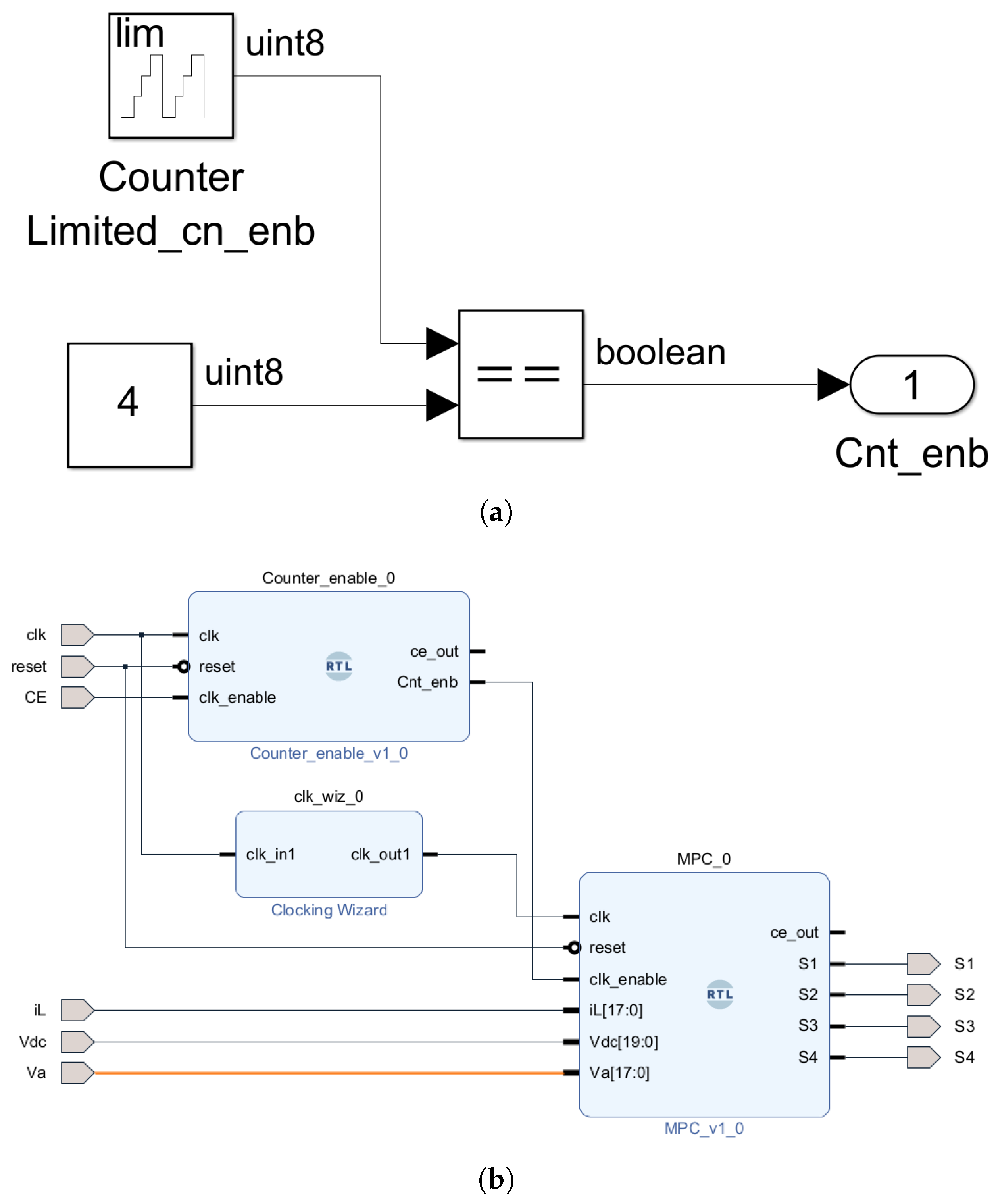
It is noteworthy that the original clock period of the board is 8 ns, and it is smaller than the desired clock period for the MPC controller. Vivado offers an IP called Clocking Wizard to perform this conversion. However, the IP output has a frequency limitation of to 800 MHz, which does not support the needed low-frequency clock (500 ns or 2 MHz) assumed for this application. The proposed solution to overcome this challenge is to incorporate the clocking wizard, achieving a clock of 10 MHz, combined with a frequency divider used for the enable of the MPC block.
Figure 10a illustrates the design of the frequency divider in HDL Coder, serving as the enable signal for the MPC block. This component acts as a frequency divider (), comprising a counter that counts from zero to four and a comparator generating a True signal when the counter reaches four. The incorporation of this block into Vivado is illustrated in Figure 10b. In this model, the Clocking Wizard IP converts the original clock to a signal with a period of 100 ns, which is then connected to the MPC block. The frequency divider block receives the clock generated by the Clocking Wizard and produces the Cnt_enb signal, which is True for 100 ns every 500 ns. The enable input of the MPC block is connected to the Cnt_enb, ensuring the execution of the MPC algorithm every 500 ns. This approach can be applied to achieve any low-frequency clock required for the controller designed in an FPGA.
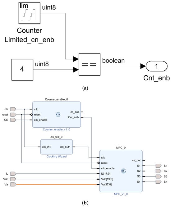
Figure 10.
The design used for execution of MPC algorithm with a step of 500 ns. (a) The frequency divider designed in HDL Coder, and (b) the design in Vivado.
After setting up the constraints, Vivado will use them to optimize the placement and routing and converts the synthesized netlist into a binary .bit file that can be loaded onto the FPGA. To complete this process in Vivado, the Generate Bitstream option is selected from the toolbar, initiating the bitstream generation process. Vivado then analyzes the design, allocates resources, and configures the FPGA accordingly. Once this process is completed the .bit file for FPGA programming will be available.
5. MPC Algorithm Verification
This section evaluates the performance of the designed MPC controller through offline MATLAB Simulink simulations and experimental HIL tests upon deployment to the FPGA. The implementation of the MPC controller for a grid-connected single-phase H-bridge converter, detailed with parameters in Table 3, was executed on a Digilent FPGA development platform (ARTY Z7). The parameters in Table 3 were chosen to ensure stable converter operation and the correct injection of 1 kW into the grid. The grid-side inductor value and DC link voltage were optimized to limit the current ripple within acceptable bounds, maintaining power quality, and achieving appropriate dynamic performance for precise tracking of the reference current waveform. The grid voltage of 110 Vrms and 50 Hz is a standard value commonly used in grid-connected power electronics applications [36,37,38,39].
Table 3.
Parameters of the H-bridge converter and the MPC algorithm.
It is important to note that the chosen sampling step of 500 ns, while small for practical applications due to the switching frequency limitations of power electronic devices, demonstrates the proposed methodology’s capability to achieve smaller sampling steps. For real-world applications, frequency control strategies such as the Period Control Approach (PCA) should be implemented to prevent excessively high switching frequencies while preserving small sampling steps. Although the selected parameters are tailored to the target application, the proposed methodology is versatile and can be adapted to other configurations, as long as they align with the system’s power and operational specifications. This flexibility underscores the robustness and scalability of the proposed approach, which is validated under practical conditions.
5.1. MATLAB Simulation
The preliminary verification involved MATLAB Simulink simulation, integrating the MPC algorithm with the SimScape model of the H-bridge converter. Figure 11 displays the controller’s dynamic response, validating the HDL Coder-designed controller’s effectiveness and the fixed-point format’s suitability for the MPC model. It is important to note that the currents shown in this figure, as well as throughout the rest of this paper, represent the averaged current per switching cycle, as it provides a clearer view of the energy transferred over time, minimizing the influence of high-frequency ripple. Figure 11a shows the controller’s ability to inject a 9.1 A rms current (calculated as ), effectively regulating the grid current to match the reference waveform for an average injected power of 1 kW. The precise tracking of the desired current trajectory by the injected current underscores the controller’s accuracy. Figure 11b illustrates the controller’s response to a sudden change in reference current from 9.1 A rms to 4.55 A rms at s, simulating a dynamic load demand or grid condition change. The controller quickly adjusts the injected current, efficiently converging to the new reference value with minimal overshoot and settling time, demonstrating the MPC algorithm’s responsiveness and robustness.
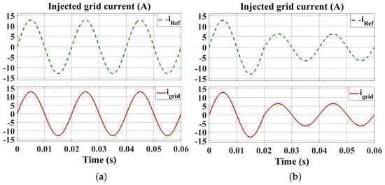
Figure 11.
Simulation results of the MPC algorithm designed in HDL Coder. (a) The averaged inductor current per switching period when , and (b) response to a step change in reference conductance from to at s.
These simulations offer insights into the MPC controller’s performance under ideal conditions, setting the stage for real-world applicability validation through FPGA-based HIL testing, as explored in the subsequent subsection.
5.2. HIL Simulation
HIL testing is essential for validating the real-world applicability and performance of the MPC controller before connecting it to a real converter. This crucial phase involves testing the controller at its final stage, where it interfaces with the HIL model and operates within the FPGA environment. This method substitutes the physical converter hardware with a simulated model on an FPGA, facilitating rapid prototyping and development by circumventing the limitations of physical setups. Moreover, the real-time nature of HIL simulation provides a more reliable representation of the converter’s behavior compared with offline simulations, while maintaining safety.
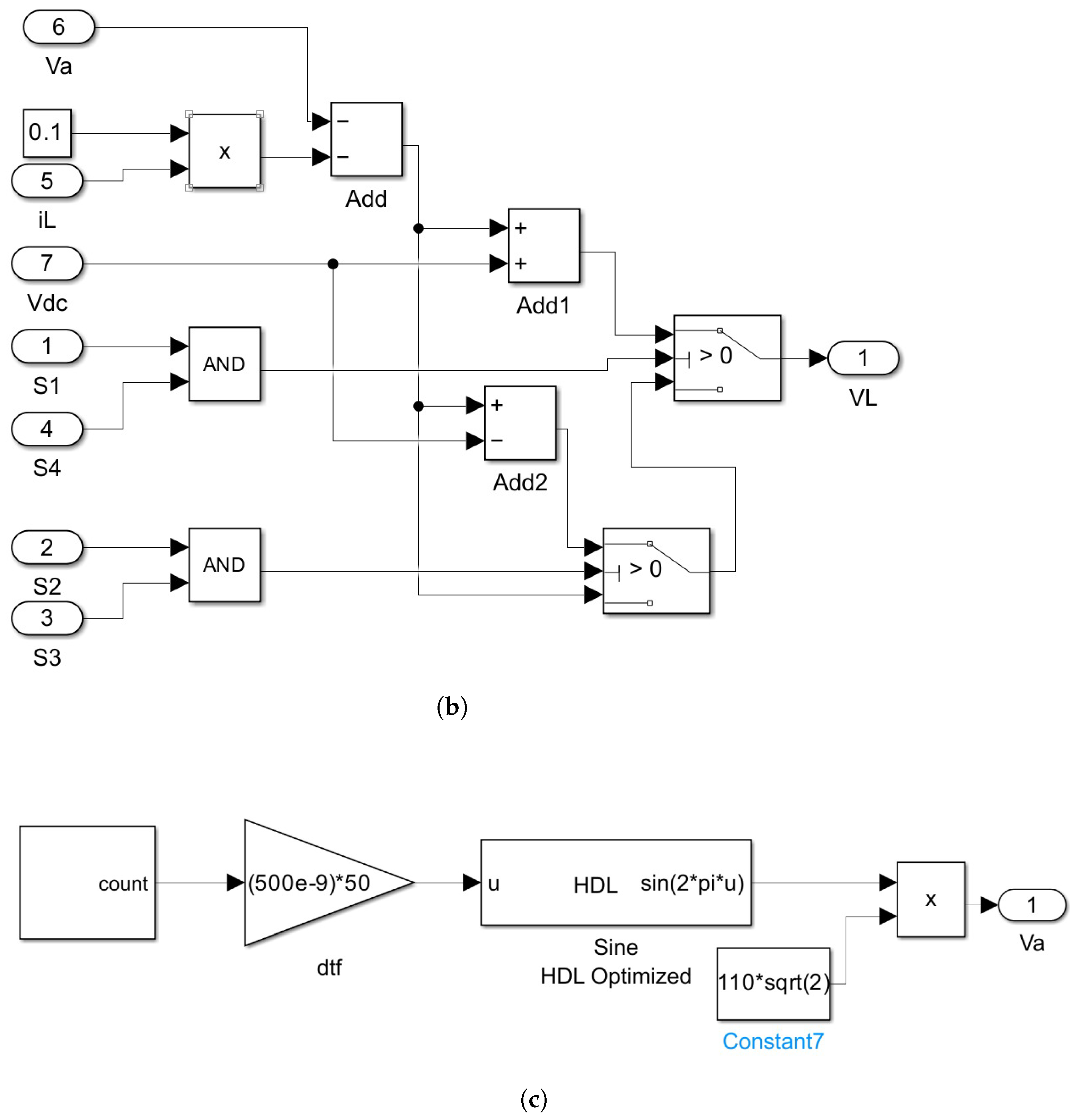
The HIL model construction begins with encoding the H-bridge converter’s governing equations into a block utilizing the HDL Coder library. Figure 12 delineates the essential components of the HIL model: Figure 12a depicts the HIL model of the H-bridge converter, where it receives switching pulses to calculate the inductor current () based on Equation (6) in accordance with the prediction block of the MPC controller. Figure 12b illustrates the inductor voltage calculation block, dynamically determining the inductor’s voltage based on the switching state. Figure 12c depicts the grid voltage generator, a custom block designed to produce the desired frequency and amplitude for the grid voltage. The ”Sine HDL Optimized” block employs a lookup table for sine waveform generation, while a counter block ensures the target grid frequency is met.
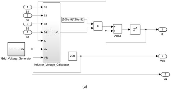

Figure 12.
The HIL model of the H-bridge designed in HDL Coder. (a) General model, (b) inductor voltage calculator block, and (c) grid voltage generator.
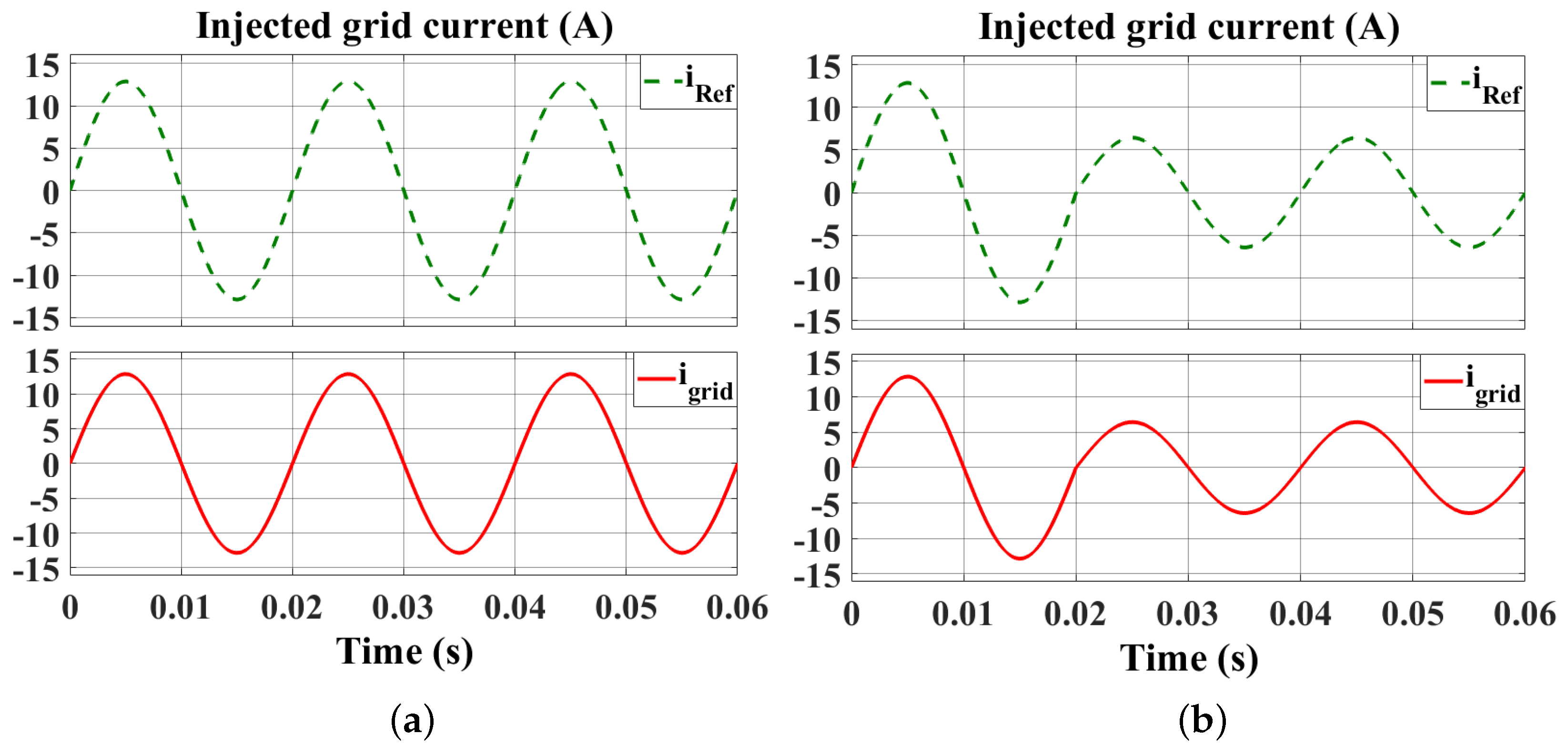
The validation of the HIL model’s fidelity involves simulations that compare its responses with those modeled in Simscape, focusing on the MPC controller’s dynamic response to the same step change in the reference current as tested before. The outcomes, depicted in Figure 13, reveal a significant resemblance between the responses from both simulations. This resemblance confirms that the HIL model, created using HDL Coder, accurately mirrors the behavior of the H-bridge converter as simulated in Simscape. This congruence underscores the HIL model’s ability to precisely emulate the physical system’s behavior in real-time, which is crucial for the ongoing testing of the MPC controller. Concurrently, the VHDL code for the entire system is generated, prepared for FPGA programming, a process detailed in Section 4. This step marks a critical transition from simulation-based validation to actual hardware implementation, facilitating a comprehensive evaluation and refinement of the controller’s performance in real-world scenarios.
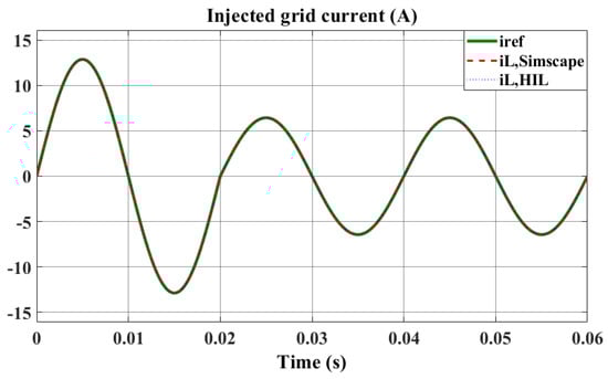
Figure 13.
HIL model MATLAB simulation results for the step change in reference current, where the currents shown represent the averaged current per switching cycle.
5.3. Experimental HIL Test
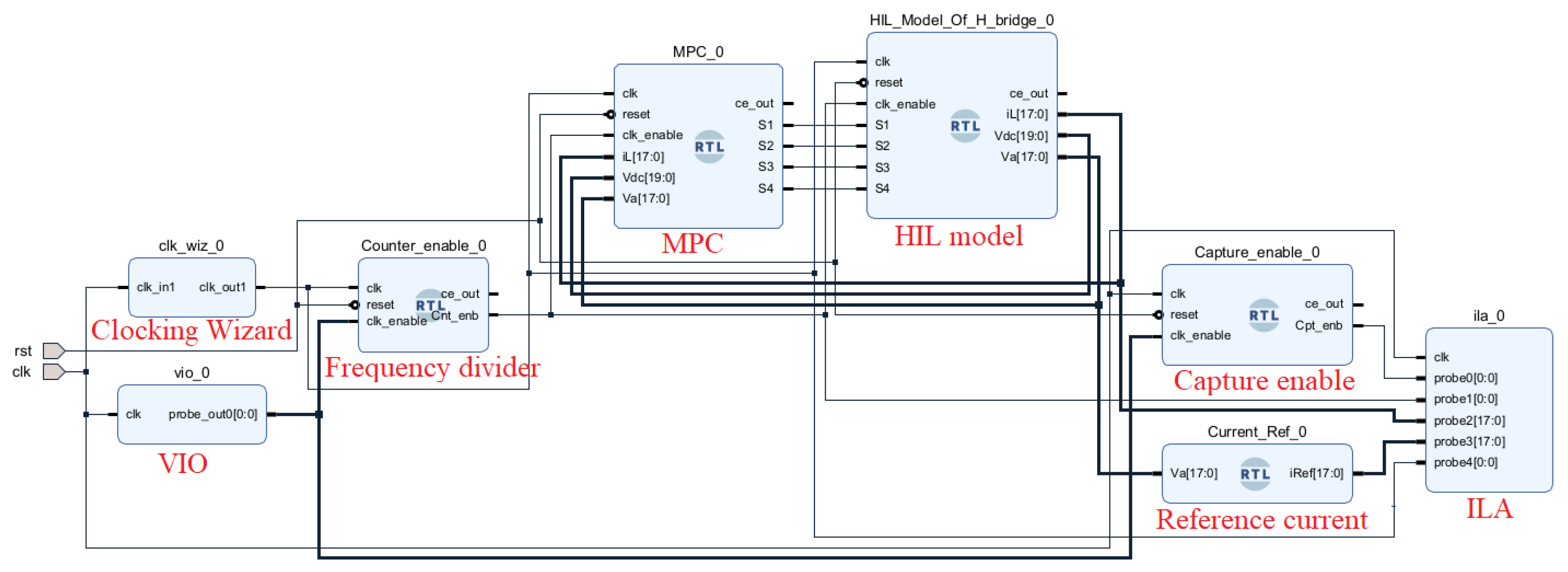
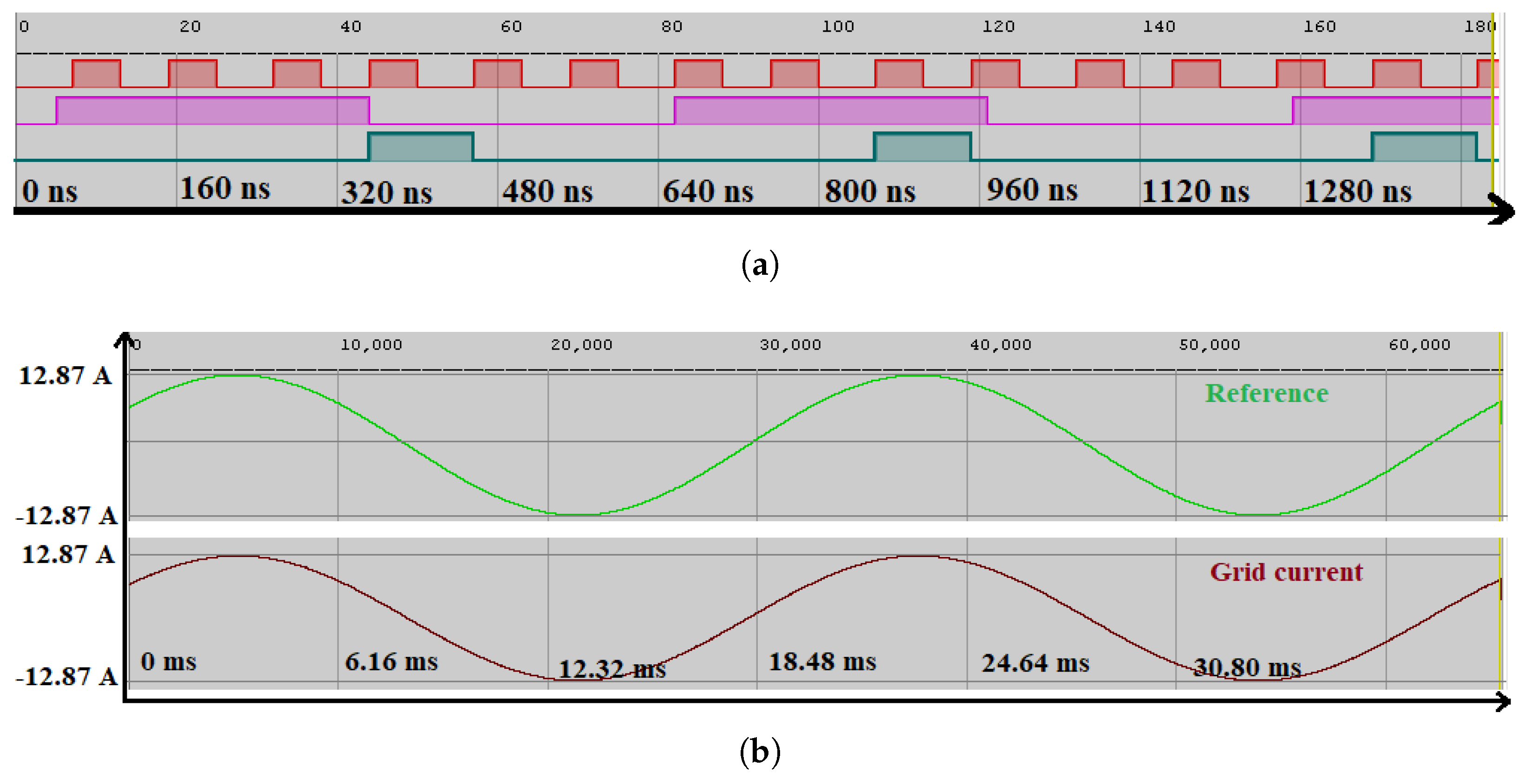
The performance of the FPGA-implemented MPC controller has to be tested in real-time with a HIL test. This process involves transferring VHDL code for the MPC controller and the single-phase H-bridge converter into the FPGA using the Vivado tool. First, the VHDL codes that represent the whole system are added to a Vivado project. The block design of the whole system is depicted in Figure 14. The capture enable block in this figure functions similarly to the previously described frequency divider. However, it generates a signal with the period of , chosen to capture two cycles of the grid current in the ILA window, which is set up to hold 65,536 data points. The integration of the ILA IP core is very important since it allows designers to access internal and target signals without the need for external testing equipment, facilitating the debugging process.
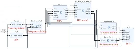
Figure 14.
The block diagram of the HIL test in Vivado tool.
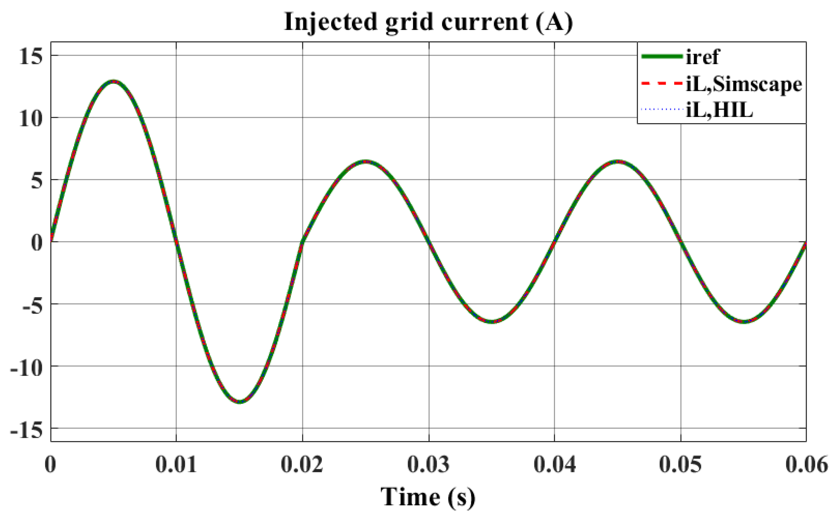
The FPGA programming process is completed by generating the .bit file in the Vivado tool from the VHDL code. It is noteworthy that the FPGA board has been selected for this project. Figure 15a demonstrates the clocking wizard’s output in red, alongside signals from the frequency divider in purple and the capture enable block in green, each distinguished by their unique periods of 100 ns, 500 ns, and 616 ns, respectively. Additionally, Figure 15b illustrates the reference and injected currents into the grid, where each sampling point is equivalent to 616 ns, and the figure is enhanced with axes for its readability. As can be ssen, the grid current follows the reference current with the amplitude of 12.86 A and frequency of 50 Hz. The result observed between simulated and real-time execution results provides strong validation of the controller’s functionality within the hardware setup.
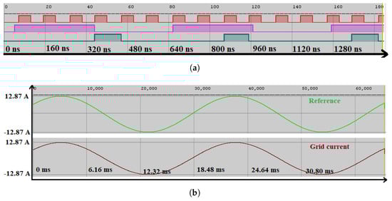
Figure 15.
Illustration of signal generation within the FPGA environment: (a) Internal signals and (b) the reference current and the injected current to the grid.
It is important to emphasize that the results presented in this figure are obtained from HIL experimental test, where the controller has been synthesized and fully implemented in an FPGA. This implementation ensures that the controller operates in its final form, incorporating almost all non-idealities that would be present in a physical prototype. For instance, the controller uses fixed-point arithmetic with the same bit precision as would be employed in its final deployment, and all algorithmic delays are exactly as they would be in a real-world implementation. Moreover, the controller has been tested in real-time operation, with a model of a full-bridge converter specifically designed and implemented in the FPGA for this purpose.
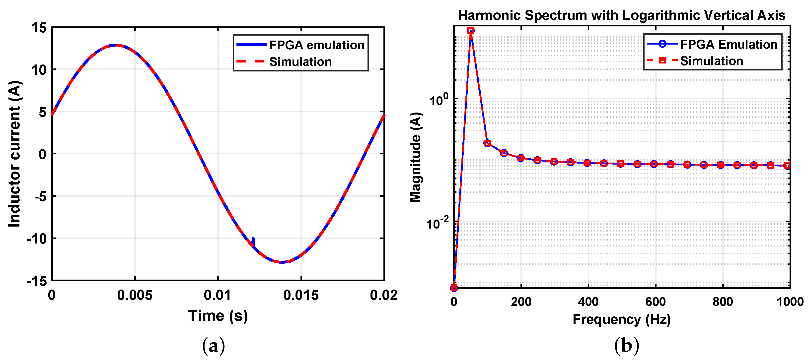
To further strengthen the validation of the developed system, a comparative analysis has been conducted between the results extracted from the ILA outputs transferred to MATLAB and the simulations performed in MATLAB Simulink HDL Coder. Figure 16a demonstrates the corresponding waveforms obtained through both methodologies. It reveals a remarkable similarity in averaged current patterns and timing characteristics, affirming the accuracy of the HDL Coder in emulating the actual hardware behavior. Additionally, an FFT analysis of these currents was performed to evaluate harmonic content. Due to the small sampling step achieved by the FPGA implementation of the controller, subharmonics are significantly minimized, as shown in Figure 16b. This coherence highlights the robustness of the design approach and ensures the applicability of the system for real-world implementations. Such comparative evaluations are crucial for bridging the gap between simulation-based development and practical deployments, providing confidence in the system’s operational integrity.
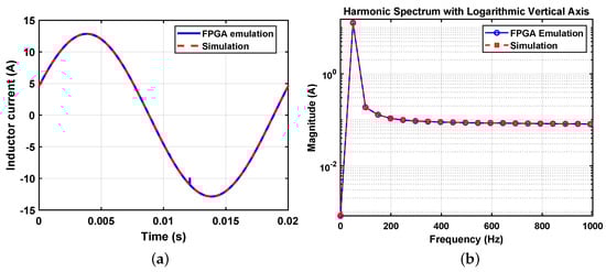
Figure 16.
Comparison of ILA experimental data and HDL Coder simulation; (a) Averaged inductor current and (b) FFT analysis.
The HIL validation, the final stage in the proposed design flow, closely reflects the performance of a physical prototype, accounting for key non-idealities such as fixed-point arithmetic and algorithmic delays. Minimal differences are expected between the HIL results and a physical implementation, with any variations likely due to noise. These factors provide strong confidence in the design readiness for real-world application.
5.4. Discussion
The stability and reliability of MPC controllers have been extensively studied in prior works, such as those by Mebkhouta et al. [40] and Cheng et al. [41] which rigorously prove the theoretical stability of such controllers under various conditions. While this study does not focus on the theoretical stability analysis, it builds upon these established foundations. The primary focus of this work is to simplify the implementation and verification processes for FPGA-based MPC controllers. By leveraging MATLAB Simulink HDL Coder, this study addresses challenges in hardware resource utilization and practical deployment rather than revisiting stability proofs. However, the simulation and hardware-in-the-loop testing conducted here confirm the practical viability of the proposed approach, ensuring robust performance in real-time applications based on the groundwork laid by these earlier stability analysis.
While the single-phase H-bridge topology is used in this study for its simplicity, the proposed methodology is adaptable to more complex systems. For instance, in three-phase H-bridge inverters, the predictive model can be extended to account for three phases and evaluate the eight possible switching states directly in the abc frame, without requiring transformations to the dq or - frames. The same principles can also be applied to other topologies, such as three-level NPC converters or five-level cascaded inverters, by appropriately extending the predictive model and cost function. This adaptability highlights the scalability of the proposed methodology, enabling its application to a wide range of power converter configurations and use cases.
While the proposed methodology demonstrates significant advancements in simplifying FPGA-based MPC implementation using MATLAB Simulink HDL Coder, several limitations should be acknowledged. The dependence on proprietary tools such as MATLAB Simulink HDL Coder may restrict accessibility for researchers or industries with budgetary constraints. This limitation could be addressed by exploring open-source or hybrid alternatives in future research to broaden the methodology’s applicability.
Another potential limitation lies in latency issues. Although the study achieves an impressive sampling step of 32 ns, achieving such performance comes at the cost of increased computational demands and hardware utilization. As Iranian et al. [35] describe, sequential methods can be employed to reduce resource utilization by reusing hardware for repeated calculations. However, this approach slightly increases the sampling step, presenting a trade-off between performance and resource efficiency.
Lastly, while the methodology is validated through simulation and HIL testing, the long-term reliability of FPGA-based implementations under diverse operating conditions remains unexplored. Future work could incorporate accelerated aging tests or real-world deployments to provide a more comprehensive analysis of system reliability over extended periods.
6. Conclusions
This paper demonstrates the feasibility and practicality of using MATLAB Simulink HDL Coder for FPGA implementation of Model Predictive Control (MPC) algorithms. By applying the methodology to a grid-connected single-phase H-bridge converter, the research highlights the advantages of this approach in simplifying FPGA programming and enabling access to engineers with limited expertise in hardware description languages. A simple case study was intentionally chosen to focus on demonstrating the proposed workflow, rather than the intricacies of the MPC algorithm itself.
However, the proposed methodology is adaptable to more complex topologies with minimal changes to the predictive model and cost function, as shown for the three-phase inverter. The study addresses the complexities of FPGA-based MPC implementation by providing a systematic framework for transitioning from conceptual design to hardware deployment.
This study highlights how the methodology achieves minimal FPGA resource utilization and a theoretical sampling step as short as 32 ns, significantly surpassing state-of-the-art implementations with sampling steps in the range of 1 s or higher. This significant performance improvement was achieved with minimal FPGA resource utilization, demonstrating the efficiency and practicality of the approach for resource-constrained devices. While the 32 ns sampling step capability was not utilized due to switching frequency limitations in power electronic devices, this capability provides an exciting opportunity for future research. Future advancements could explore integrating MPC methods that directly control the switching frequency such as PCA method, enabling the full utilization of smaller sampling steps. Furthermore, early-stage simulations integrating the MPC algorithm with the converter model in Simscape allowed potential issues to be identified and resolved before hardware implementation, reducing development time and simplifying the debugging process. Validation through MATLAB simulations and hardware-in-the-loop (HIL) experimental tests confirmed the reliability and precision of the MPC controller in regulating grid current under dynamic load conditions. The real-time FPGA implementation not only demonstrated technical feasibility but also proved the operational robustness of the controller, highlighting its suitability for high-frequency power electronics applications.
The proposed approach bridges the gap between complex control algorithms and real-world hardware implementation, providing an efficient and scalable solution for FPGA-based MPC systems. Future research could extend this methodology to multi-phase systems and other advanced control strategies, further broadening its applicability in industrial and power electronics domains.
Author Contributions
Conceptualization, M.P.; Formal analysis, M.P. and E.Z.; Funding acquisition, A.d.C.; Investigation, M.P. and E.Z.; Methodology, E.Z.; Project administration, A.d.C.; Software, M.P.; Supervision, A.d.C.; Validation, E.Z. and A.d.C.; Writing—original draft, M.P.; Writing—review and editing, E.Z. and A.d.C. All authors have read and agreed to the published version of the manuscript.
Funding
This research has been partially funded by the project PID2022-137593OBI00, financed by the Spanish Ministry MCIN/AEI/10.13039/501100011033/FEDER, UE, and FSE+.
Institutional Review Board Statement
Not applicable.
Informed Consent Statement
Not applicable.
Data Availability Statement
Further data and additional details related to this study are available upon request.
Conflicts of Interest
The authors declare no conflicts of interest.
References
- Chu, S.; Wang, B.; Niu, X. Simplified Reactive Torque Model Predictive Control of Induction Motor with Common Mode Voltage Suppression. IEICE Trans. Electron. 2023, 30, 132–140. [Google Scholar] [CrossRef]
- Kouro, S.; Cortes, P.; Vargas, R.; Ammann, U.; Rodriguez, J. Model Predictive Control—A Simple and Powerful Method to Control Power Converters. IEEE Trans. Ind. Electron. 2009, 56, 1826–1838. [Google Scholar] [CrossRef]
- Vazquez, S.; Rodriguez, J.; Rivera, M.; Franquelo, L.G.; Norambuena, M. Model Predictive Control for Power Converters and Drives: Advances and Trends. IEEE Trans. Ind. Electron. 2017, 64, 935–947. [Google Scholar] [CrossRef]
- Garcia-Torres, F.; Zafra-Cabeza, A.; Silva, C.; Grieu, S.; Darure, T.; Estanqueiro, A. Model Predictive Control for Microgrid Functionalities: Review and Future Challenges. Energies 2021, 14, 1296. [Google Scholar] [CrossRef]
- Karamanakos, P.; Liegmann, E.; Geyer, T.; Kennel, R. Model Predictive Control of Power Electronic Systems: Methods, Results, and Challenges. IEEE Open J. Ind. Appl. 2020, 1, 95–114. [Google Scholar] [CrossRef]
- Ahmed, A.A.; Koh, B.K.; Lee, Y.I. A Comparison of Finite Control Set and Continuous Control Set Model Predictive Control Schemes for Speed Control of Induction Motors. IEEE Trans. Ind. Inform. 2018, 14, 1334–1346. [Google Scholar] [CrossRef]
- Preindl, M.; Bolognani, S. Comparison of direct and PWM model predictive control for power electronic and drive systems. In Proceedings of the Twenty-Eighth Annual IEEE Applied Power Electronics Conference and Exposition (APEC), Long Beach, CA, USA, 17–21 March 2013; pp. 2526–2533. [Google Scholar]
- Baier, C.R.; Ramirez, R.O.; Marciel, E.I.; Hernández, J.C.; Melín, P.E.; Espinosa, E.E. FCS-MPC Without Steady-State Error Applied to a Grid-Connected Cascaded H-Bridge Multilevel Inverter. IEEE Trans. Power Electron. 2021, 36, 11785–11799. [Google Scholar] [CrossRef]
- Xue, C.; Ding, L.; Li, Y. CCS-MPC with Long Predictive Horizon for Grid-Connected Current Source Converter. In Proceedings of the IEEE Energy Conversion Congress and Exposition (ECCE), Detroit, MI, USA, 11–15 October 2020; pp. 4988–4993. [Google Scholar]
- Sanchez, P.M.; Machado, O.; Peña, E.J.; Rodríguez, F.J.; Meca, F.J. FPGA-Based Implementation of a Predictive Current Controller for Power Converters. IEEE Trans. Ind. Inform. 2013, 9, 1312–1321. [Google Scholar] [CrossRef]
- Sepúlveda, C.A.; Muñoz, J.A.; Espinoza, J.R.; Figueroa, M.E.; Baier, C.R. FPGA v/s DSP Performance Comparison for a VSC-Based STATCOM Control Application. IEEE Trans. Ind. Inform. 2013, 9, 1351–1360. [Google Scholar] [CrossRef]
- Monmasson, E.; Cirstea, M.N. FPGA Design Methodology for Industrial Control Systems—A Review. IEEE Trans. Ind. Electron. 2007, 54, 1824–1842. [Google Scholar] [CrossRef]
- Takasu, R.; Tomioka, Y.; Ishigaki, Y.; Li, N.; Shibata, T.; Nakanishi, M.; Kitazawa, H. An FPGA Implementation of the Two-Dimensional FDTD Method and Its Performance Comparison with GPGPU. IEICE Trans. Electron. 2014, E97-C, 697–706. [Google Scholar] [CrossRef]
- Cirugeda-Roldán, E.M.; Martínez-García, M.S.; Sanchez, A.; de Castro, A. Evaluation of the Different Numerical Formats for HIL Models of Power Converters after the Adoption of VHDL-2008 by Xilinx. Electronics 2021, 10, 1952. [Google Scholar] [CrossRef]
- Lamo, P.; de Castro, A.; Sanchez, A.; Ruiz, G.A.; Azcondo, F.J.; Pigazo, A. Hardware-in-the-Loop and Digital Control Techniques Applied to Single-Phase PFC Converters. Electronics 2021, 10, 1563. [Google Scholar] [CrossRef]
- Schafer, B.C.; Iguchi, Y.; Takahashi, W.; Nagatani, S.; Wakabayashi, K. Fixed Point Data Type Modeling for High Level Synthesis. IEICE Trans. Electron. 2010, E93-C, 361–368. [Google Scholar] [CrossRef]
- Nane, R.; Sima, V.M.; Pilato, C.; Choi, J.; Fort, B.; Canis, A.; Bertels, K. A Survey and Evaluation of FPGA High-Level Synthesis Tools. IEEE Trans. Comput.-Aided Des. Integr. Circuits Syst. 2016, 35, 1591–1604. [Google Scholar] [CrossRef]
- Estrada, L.; Vázquez, N.; Vaquero, J.; de Castro, Á.; Arau, J. Real-Time Hardware in the Loop Simulation Methodology for Power Converters Using LabVIEW FPGA. Energies 2020, 13, 373. [Google Scholar] [CrossRef]
- Saralegui, R.; Sanchez, A.; de Castro, A. Efficient Hardware-in-the-Loop Models Using Automatic Code Generation with MATLAB/Simulink. Electronics 2023, 12, 2786. [Google Scholar] [CrossRef]
- Zamiri, E.; Sanchez, A.; Yushkova, M.; Martínez-García, M.S.; de Castro, A. Comparison of Different Design Alternatives for Hardware-in-the-Loop of Power Converters. Electronics 2021, 10, 926. [Google Scholar] [CrossRef]
- Iranian, M.E.; Mohseni, M.; Aghili, S.; Parizad, A.; Baghaee, H.R.; Guerrero, J.M. Real-Time FPGA-Based HIL Emulator of Power Electronics Controllers Using NI PXI for DFIG Studies. IEEE J. Emerg. Sel. Top. Power Electron. 2020, 10, 2005–2019. [Google Scholar] [CrossRef]
- Singh, V.K.; Tripathi, R.N.; Hanamoto, T. FPGA-Based Implementation of Finite Set-MPC for a VSI System Using XSG-Based Modeling. Energies 2020, 13, 260. [Google Scholar] [CrossRef]
- Mishra, I.; Tripathi, R.N.; Singh, V.K.; Hanamoto, T. Step-by-Step Development and Implementation of FS-MPC for a FPGA-Based PMSM Drive System. Electronics 2021, 10, 395. [Google Scholar] [CrossRef]
- Singh, V.K.; Tripathi, R.N.; Hanamoto, T. Implementation Strategy for Resource Optimization of FPGA-Based Adaptive Finite Control Set-MPC Using XSG for a VSI System. IEEE J. Emerg. Sel. Top. Power Electron. 2021, 9, 2066–2078. [Google Scholar] [CrossRef]
- Marmol, A.; Zamiri, E.; Purraji, M.; Murillo, D.; Díaz, J.T.; Vazquez, A.; de Castro, A. Dual Control Strategy for Non-Minimum Phase Behavior Mitigation in DC-DC Boost Converters Using Finite Control Set Model Predictive Control and Proportional–Integral Controllers. Appl. Sci. 2024, 14, 10318. [Google Scholar] [CrossRef]
- Nasika, D.; Yuvaraju, A.; Reddy, V.K.; Sundar, S.V.N.J. FPGA-In-Loop Simulation of an Improved Converter Firing Control for LCC HVDC and Validation Using Real-Time Digital Simulator (HIL). In Proceedings of the 2019 IEEE International Conference on Electrical, Computer and Communication Technologies (ICECCT), Coimbatore, India, 20–22 February 2019; pp. 1–8. [Google Scholar]
- Singh, V.K.; Tripathi, R.N.; Hanamoto, T. Model-based design approach for implementation of finite state MPC. In Proceedings of the 13th IEEE Conference on Industrial Electronics and Applications (ICIEA), Wuhan, China, 31 May–2 June 2018; pp. 881–886. [Google Scholar]
- Siwakoti, Y.P.; Town, G.E. Design of FPGA-controlled power electronics and drives using MATLAB Simulink. In Proceedings of the IEEE ECCE Asia Downunder, Melbourne, VIC, Australia, 3–6 June 2013; pp. 571–577. [Google Scholar]
- Sankar, D.; Syamala, L.; Chembathu Ayyappan, B.; Kallarackal, M. FPGA-Based Cost-Effective and Resource Optimized Solution of Predictive Direct Current Control for Power Converters. Energies 2021, 14, 7669. [Google Scholar] [CrossRef]
- Yushkova, M.; Sanchez, A.; de Castro, A. Strategies for choosing an appropriate numerical method for FPGA-based HIL. Int. J. Electr. Power Energy Syst. 2021, 132, 107186. [Google Scholar] [CrossRef]
- Cong, J.; Liu, B.; Neuendorffer, S.; Noguera, J.; Vissers, K.; Zhang, Z. High-Level Synthesis for FPGAs: From Prototyping to Deployment. IEEE Trans. Comput.-Aided Des. Integr. Circuits Syst. 2011, 30, 473–491. [Google Scholar] [CrossRef]
- Zamiri, E.; Sanchez, A.; de Castro, A.; Martínez-García, M.S. Comparison of Power Converter Models with Losses for Hardware-in-the-Loop Using Different Numerical Formats. Electronics 2019, 8, 1255. [Google Scholar] [CrossRef]
- Aguirre, M.; Vazquez, S.; Alcaide, A.M.; Portillo, R.; Kouro, S.; Leon, J.I.; Franquelo, L.G. Period Control Approach Finite Control Set Model Predictive Control Switching Phase Control for Interleaved DC/DC Converters. IEEE Trans. Ind. Electron. 2024, 71, 8304–8312. [Google Scholar] [CrossRef]
- Montazeri, A.; König, O.; Griepentrog, G. Investigating Effects of Delta-Sigma Modulation for Current Measurement on FCS-MPC of IM: Hardware in the Loop Results. In Proceedings of the 2017 IEEE International Symposium on Predictive Control of Electrical Drives and Power Electronics (PRECEDE), Pilsen, Czech Republic, 4–6 September 2017; pp. 7–12. [Google Scholar]
- Iranian, M.E.; Zamiri, E.; de Castro, A. Optimal Implementation of d-q Frame Finite Control Set Model Predictive Control with LabVIEW. Electronics 2025, 14, 100. [Google Scholar] [CrossRef]
- Srinivasan, G.K.; Rivera, M.; Loganathan, V.; Ravikumar, D.; Mohan, B. Trends and Challenges in Multi-Level Inverter with Reduced Switches. Electronics 2021, 10, 368. [Google Scholar] [CrossRef]
- Aouichak, I.; Jacques, S.; Bissey, S.; Reymond, C.; Besson, T.; Le Bunetel, J.-C. A Bidirectional Grid-Connected DC–AC Converter for Autonomous and Intelligent Electricity Storage in the Residential Sector. Energies 2022, 15, 1194. [Google Scholar] [CrossRef]
- Beser, E.; Arifoglu, B.; Camur, S.; Beser, E.K. A grid-connected photovoltaic power conversion system with single-phase multilevel inverter. Sol. Energy 2010, 84, 2056–2067. [Google Scholar] [CrossRef]
- Nguyen, M.-K.; Tran, T.-T. A Single-Phase Single-Stage Switched-Boost Inverter With Four Switches. IEEE Trans. Power Electron. 2018, 33, 6769–6781. [Google Scholar] [CrossRef]
- Mebkhouta, T.; Golea, A.; Boumaraf, R.; Benchouia, T.M.; Karboua, D.; Bajaj, M.; Chebaani, M.; Blazek, V. Sensorless finite set predictive current control with MRAS estimation for optimized performance of standalone DFIG in wind energy systems. Results Eng. 2024, 24, 103622. [Google Scholar] [CrossRef]
- Cheng, Z.; Liu, Y.; Luo, B.; Zhang, Y. Improved vector selection model predictive control strategy for quasi-Z-source inverter virtual synchronous generator grid-connected system. J. Eng. 2024, 2024, e70034. [Google Scholar] [CrossRef]


Disclaimer/Publisher’s Note: The statements, opinions and data contained in all publications are solely those of the individual author(s) and contributor(s) and not of MDPI and/or the editor(s). MDPI and/or the editor(s) disclaim responsibility for any injury to people or property resulting from any ideas, methods, instructions or products referred to in the content. |
© 2025 by the authors. Licensee MDPI, Basel, Switzerland. This article is an open access article distributed under the terms and conditions of the Creative Commons Attribution (CC BY) license (https://creativecommons.org/licenses/by/4.0/).