Article

Design Strategies for BCAT Structures: Enhancing DRAM Reliability and Mitigating Row Hammer Effect

1
School of Electronic and Electrical Engineering, Kyungpook National University, Daegu 41566, Republic of Korea
2
Division of Materials Science and Engineering, Hanyang University, Seoul 04763, Republic of Korea
*
Authors to whom correspondence should be addressed.
Electronics 2025, 14(3), 499; https://doi.org/10.3390/electronics14030499
Submission received: 22 December 2024 / Revised: 15 January 2025 / Accepted: 23 January 2025 / Published: 26 January 2025
(This article belongs to the Section Semiconductor Devices)

Abstract

:
This study investigates the impact of four parameters—gate angles, fin height controlled through gate overlaps and the distance from fin to source/drain, and substrate bottom doping concentration—on the row hammer effect (RHE) in DRAM cells. The influence of adjacent and passing gates on the DRAM cell body potential was identified as a key factor in D0 and D1 failures. The tolerance for D1 and D0 failures was analyzed, defined as the threshold number of pulses required to induce a 0.6 V change in the storage node voltage (from 1.2 V to 0.6 V for a D1 failure or from 0 V to 0.6 V for a D0 failure). D1 (D0) failure tolerances with the slope from the top of the top gate (θangle) of 3°, the height of the TiN gate covering the fin (Hfin_overlap) of 12.5 nm, and the height of the fin (Hfin) of 12.5 nm are 1.26 × 10⁶ (4.8 × 10⁶), 1.14 × 10⁶ (4 × 10⁷), and 7.5 × 10⁵ (4.8 × 10⁵), respectively. Higher θangles and smaller fin heights generally result in higher RHE tolerances. Although decreasing the fin height reduced the RHE, it also decreased the on-current and resulted in an increase in the threshold voltage (VT) and the subthreshold swing (SS). In addition, by increasing the substrate bottom doping concentration (Pdop_bot), we improve RHE tolerance twice its original level without reducing the on-current. Therefore, designing a buried channel array transistor (BCAT) structure requires careful consideration of these trade-offs, and a thorough understanding of the underlying mechanism is crucial to devising strategies that reduce RHE tolerance. The findings of this study are expected to contribute significantly to the development of next-generation DRAM architectures, enhancing stability and performance. By addressing the reliability challenges posed by advanced scaling, this study paves the way for the ongoing advancement of DRAM technology for high-density and high-performance applications.

1. Introduction

Advances in the miniaturization of dynamic random access memory (DRAM) components have significantly enhanced performance and increased density, representing key milestones in semiconductor technology. However, the aggressive scaling of DRAM has resulted in significant reliability challenges that threaten the integrity and functionality of these devices [1,2,3]. Among other issues, the row hammer effect (RHE) has become a growing concern. RHE refers to the repeated activation of a particular word line in a DRAM, which can induce unintended charge loss into neighboring word lines and potentially result in data corruption. As DRAMs become denser, the spacing between cells becomes tighter, making them more vulnerable to electrical interference. Therefore, if a word line is accessed very quickly and frequently, there is an increased risk that charge loss builds up in cells adjacent to that word line, causing a bit flip. This impact threatens the reliability of circuit-level DRAMs and fabricated buried channel array transistor (BCAT) structures due to the RHE [4,5]. Two types of RHEs—D1 failures, characterized by data flipping from 1 to 0, and D0 failures, characterized by data flipping from 0 to 1—present two critical challenges in DRAM technology. D1 failure occurs when repeated access to a row of memory cells disturbs adjacent rows, causing unintended bit flips [6,7,8]. Conversely, D0 failure arises from parasitic coupling and interference between pass gates, leading to leakage currents and potential data corruption [9,10]. In addition to compromising the reliability of DRAM, this phenomenon can also leave serious system-wide vulnerabilities from a security perspective. For example, scenarios have been proposed where an attacker deliberately targets specific cells to flip bits in neighboring cells to compromise data integrity [11]. Currently, there is extensive research on reducing bit flip through systematic solutions such as error correcting codes (ECCs) to prevent bit flip due to row hammer at the software and system level [12,13,14]. However, on the device side, there is a lack of research on analyzing and optimizing D0 and D1 failures due to RHE. Furthermore, although certain studies have identified the limitations of gate formation in BCAT DRAM structures—either by applying angled gates in simulations or by examining actual TEM images— research considering these findings to address D0 and D1 failures caused by the RHE is still limited and insufficient [15,16,17,18].
In this paper, we investigate the electrical characteristics and reliability of the RHE in DRAM cells with geometric and doping modifications using TCAD Sentaurus simulations from Synopsys. This study explains the causes of row hammer in DRAM cell arrays and the pulse operation schemes of single row hammer D1 (SH D1) and D0 (SH D0), while evaluating key parameters in the BCAT structure. We extensively analyze the structural parameters of DRAM cells, focusing on the gate angle, shaped by aspect ratio limitations; the height of the TiN gate covering the fin, which directly contributes to the RHE; and variations in bottom substrate doping, affecting electron migration. Additionally, the transient and DC characteristics of these four parameters are analyzed to evaluate the performance of DRAM cells and D0/D1 failures within the DRAM array. By examining their impact on device performance and reliability, we derive practical implications for future process and design optimization.

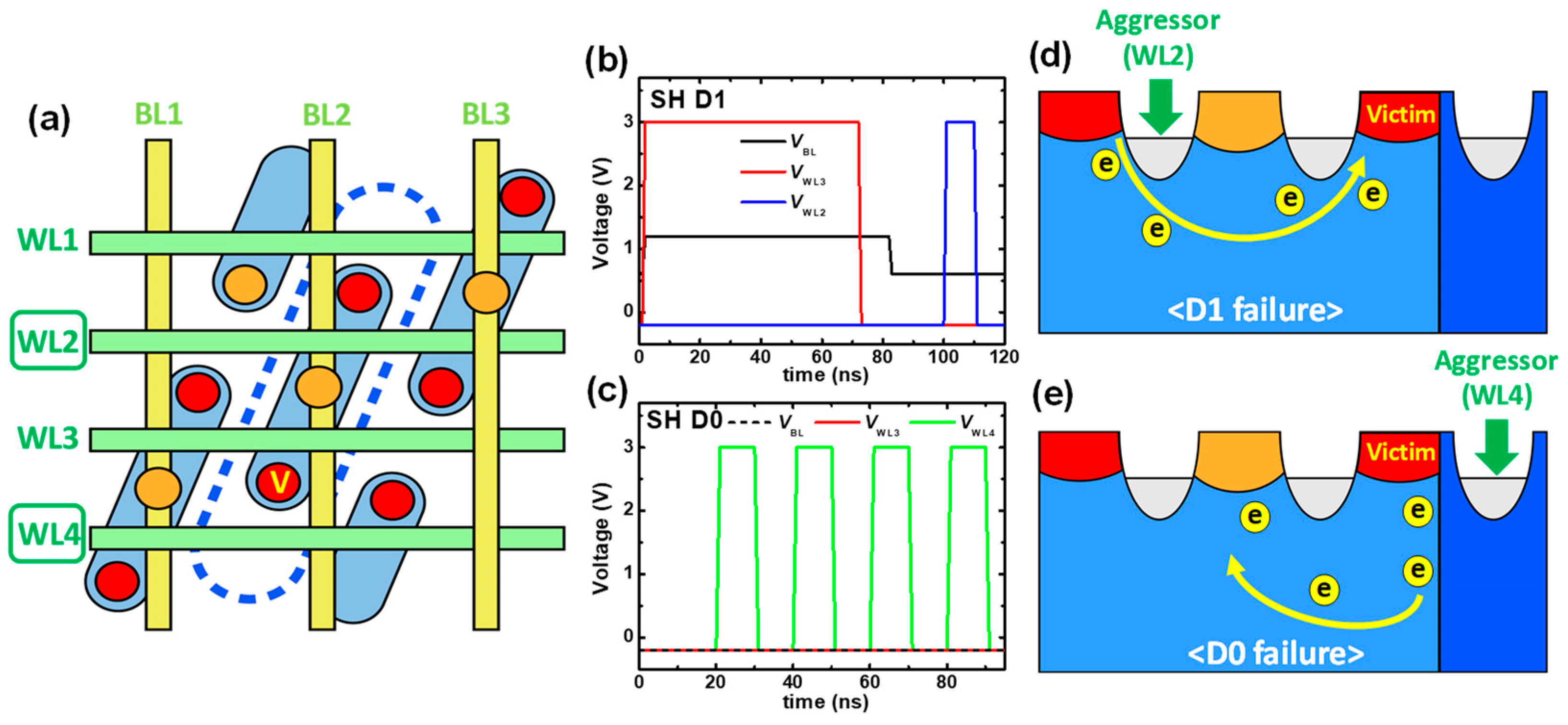
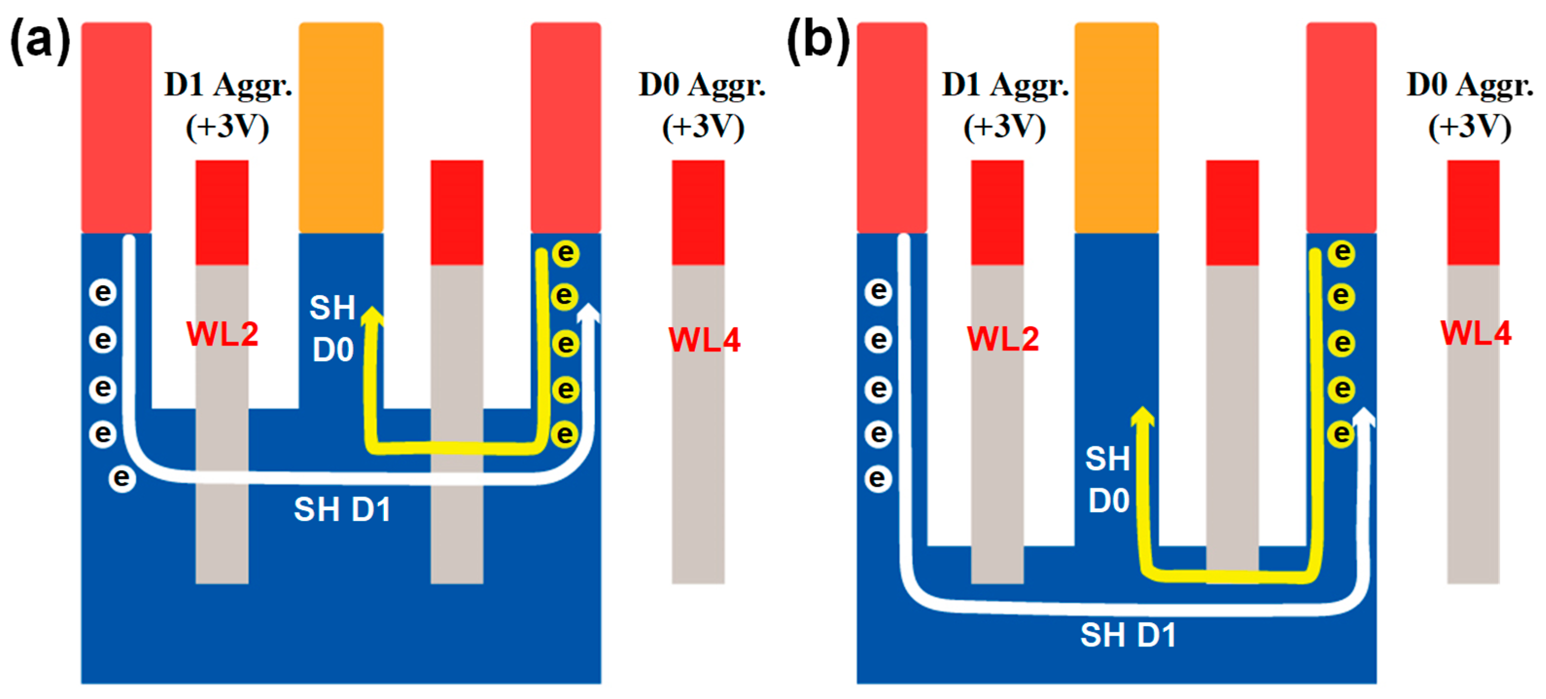
2. Device Structure and Mechanism

Figure 1a shows the 3D structure of the saddle-FinFET in DRAM cells using a TCAD simulation. To represent the detailed DRAM cell structure, cross-sectional views of the saddle-FinFET along C2-C2′ (Figure 1b) and C3-C3′ (Figure 1c) are provided, with a particular focus on parameters such as the slope from the top of the top gate (θangle), the height of the TiN gate covering the fin (Hfin_overlap), the height of the fin (Hfin), and the substrate bottom doping concentration (Pdop_bot). The corresponding device parameters, along with their respective values, are presented in Table 1. This simulation follows the structural parameters of the 10 nm-class technology of saddle-FinFET DRAM [19]. This BCAT structure uses a double gate, and the top metal gate uses n+ poly-Si doped at a concentration of 1020 cm−3 with an electron affinity of 4.0 eV to reduce gate-induced drain leakage (GIDL), and the bottom gate metal uses TiN with a large work function of 4.6 eV to increase VT to minimize leakage current and low gate resistance [20]. In this simulation, the non-local path band-to-band tunneling model was adopted to accurately model GIDL current. The doping-dependent mobility model with high field saturation and Lombardi interface charge effects was applied to account for carrier mobility. Recombination processes were modeled using the Shockley–Read–Hall (SRH) recombination model with doping-dependent parameters.
Figure 2a shows a diagram of the DRAM cell array depicting the RHE. Figure 2b illustrates the pulse scheme for single hammer D1 (SH D1), while Figure 2c represents the pulse scheme for single hammer D0 (SH D0). In the SH D1 scheme, the write ‘1’ voltages are applied to the WL3 and BL to write ‘1’ in the cell capacitor (D1, 1.2 V in storage node). Subsequently, repetitive pulses with a 22 ns period (tr = 1 ns, tf = 1 ns, ton = 10 ns, toff = 10 ns) are applied to the WL2 (aggressor). In the SH D0, the write ‘0’ voltages are applied to the WL2 and BL, as the data are initially set to ‘0’ in the cell capacitor (D0, 0 V in storage node). Then, repetitive pulses with a 22 ns period (tr = 1 ns, tf = 1 ns, ton = 10 ns, toff = 10 ns) are applied to the WL4 (aggressor). In practice, the row active time (tRAS) value of DRAM is in the range of tens of nanoseconds. However, to observe effective difference based on parameter modulations, the on/off times of the word line and associated timings were considered shorter in this study. Figure 2d shows the D1 failure mechanism, which occurs in DRAM devices when repeated access to a specific word line (the aggressor, WL2) induces disturbances in an adjacent storage node (the victim). This disturbance results from charge loss caused by frequent activation of the aggressor (WL2), potentially leading to unintended bit flip in the nearby victim cell. This phenomenon is particularly pronounced in modern DRAM technologies with smaller process nodes, where the reduced physical distance between cells increases the likelihood of interference, thereby compromising data integrity and security [21]. Figure 2e shows the D0 failure mechanism, which arises from capacitive coupling between neighboring word lines (WL4). When a word line is activated, the resulting electric field can influence neighboring lines, causing unintended disturbances [22]. These disturbances can shift the threshold voltage of nearby victim cells, potentially leading to data errors. As DRAM technology scales down, the susceptibility to coupling-induced error increases, thereby worsening the problem. Building on these insights, the mechanisms of SH D1, where data change from 1 to 0 due to the influence of adjacent gates, and SH D0, where data shift from 0 to 1 due to the influence of pass gates, underscore significant reliability challenges in memory devices.

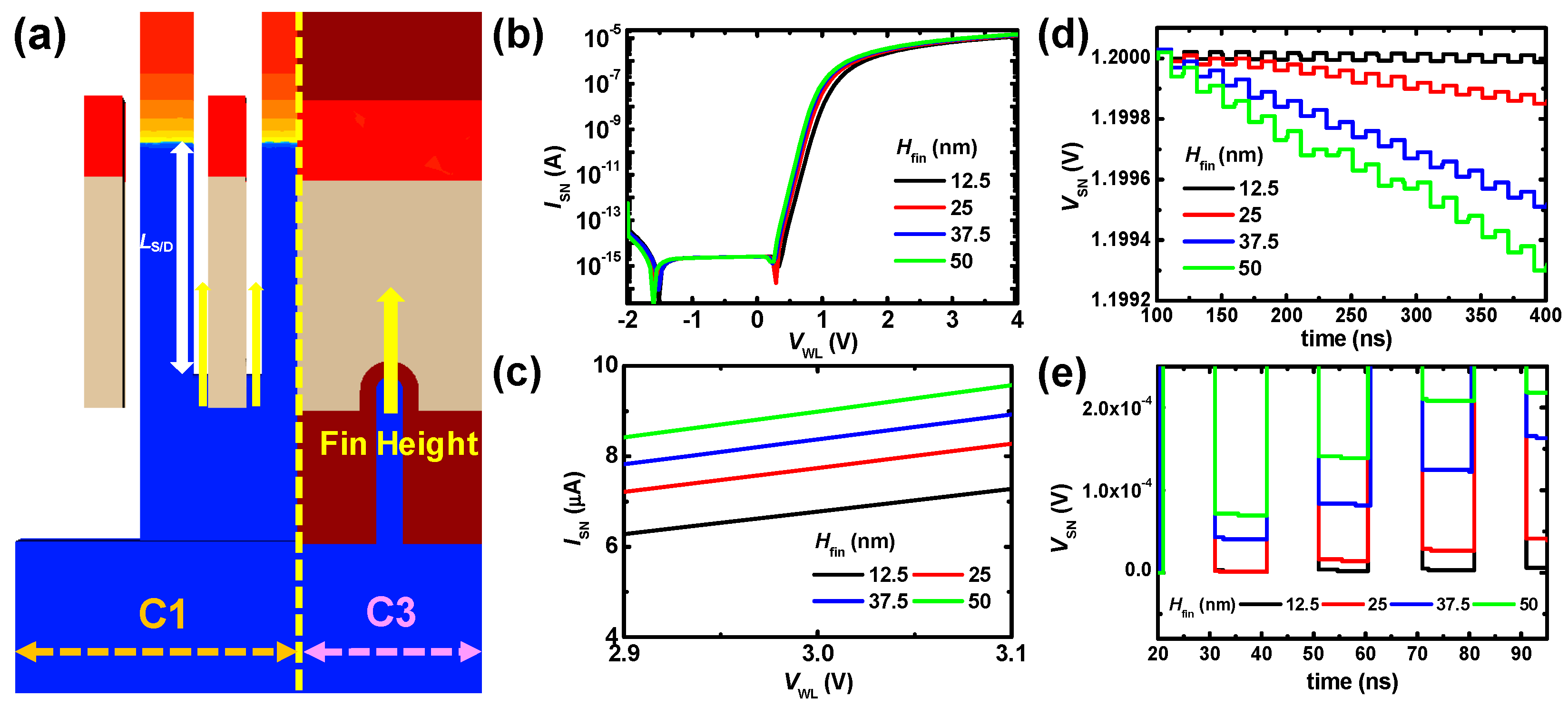
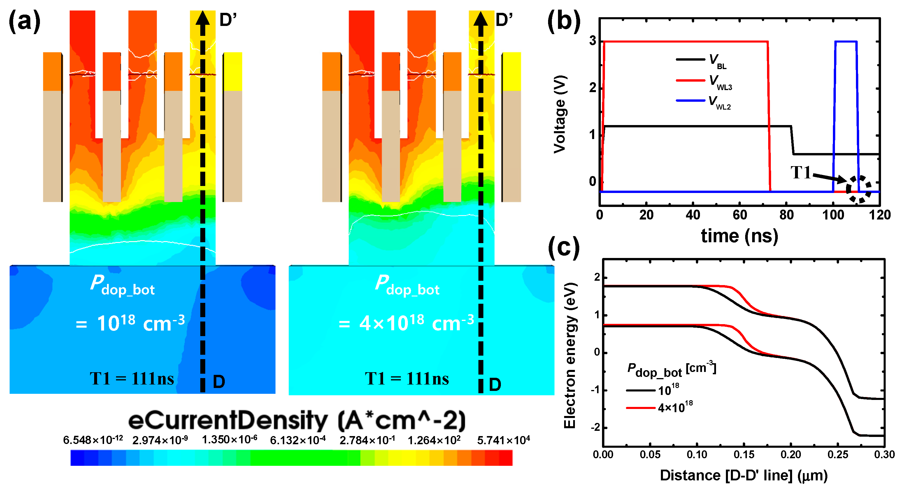
3. Analysis of Characteristics Through BCAT Structure Modifications

To address reliability degradation caused by row hammer, the BCAT structure of DRAM cell should be investigated by varying key structural parameters related to D0 and D1 failures. First, the effect of the θangle on D0 and D1 failures is analyzed as the θangle increases from 0° to 3°, considering the limitation aspect ratio in DRAM miniaturization processes, as shown in Figure 3a. In Figure 3a, the left image shows the DRAM cell with the shallow trench isolation (STI) and gate oxide, both composed of SiO2, removed along the C1-C1′ line, while the right image shows a cross-section along the C2-C2′ line. Figure 3b,c show that the DRAM cell with a θangle of 3° achieved the highest on-current at VWL = 3 V. As shown in Figure 4a,b, the channel length of a DRAM cell decreases from 126 nm at a θangle of 0° to 116 nm at a θangle of 3°, while the width remains constant. Consequently, as the θangle increases, the channel length of the DRAM cell decreases, resulting in an increase in on-current at the same feature size. Figure 3d,e illustrate the effects of D1 failure and D0 failure under varying θangle from 0° to 3°. The initial potential of the storage node (VSN) was set to 1.2 V for D1 failure and 0 V for D0 failure, respectively. As summarized in Table 2, the gate area decreases with increasing θangle, which reduces the impact of the gates on the channel or body of the DRAM cell. Figure 4c and Table 2 show that the distance between adjacent fins (Lfins) increases from 22 nm to 33 nm as the θangle increases, thereby improving tolerance. This adjustment enhances device robustness against D1 and D0 failures. The results show that increasing the θangle reduced the impact of both D1 failure and D0 failure.
Figure 5a shows the geometric modification of a DRAM cell with varying gate overlap lengths. Similar to Figure 3, the left image of Figure 5a shows the DRAM cell with the SiO2 removed along the C1-C1′ line, while the right image shows a cross-section along the C3-C3′ line. Figure 5b,c show that as Hfin_overlap increases from 12.5 to 50 nm, the on-current also increases, indicating improved gate controllability with a larger Hfin_overlap. Figure 5d,e show the vulnerability of DRAM cells to D1 failure and D0 failure at the highest Hfin_overlap, following the trend that increased gate overlap leads to greater gate controllability and influence over adjacent gates.
In Figure 6, electrical characteristics of the DRAM cell are analyzed by adjusting the U-shaped fin length to control Hfin, which induces variations in the distances from the source/drain regions to top of fins (LS/D). In the same way as the previously discussed structural modification illustrations, Figure 6a shows cross-sectional views along C1-C1′ and C3-C3′ of simulated DRAM cells with LS/D, where Hfin = 12.5 nm. Figure 6b,c show simulated ISN-VWL curves of DRAM cells as a parameter of Hfins. The on-current of DRAM cells increases because the channel length decreases as Hfin increases from 12.5 to 50 nm. Operating mechanisms of the D1 and D0 failure with different Hfins (50 nm and 12.5 nm) are investigated in Figure 7. When aggressive signals are applied through the WL2 (aggressor), the electrons that should flow into the bit line node are diverted to the victim node on the right. As shown in Figure 7, the LS/D decreases as the Hfin increases, leading to a higher current flow. Consequently, more electrons are transported, increasing the number of electrons crossing over to the victim cell, which worsens the occurrence of D1 failure. Furthermore, when examining the D0 failure phenomenon, applying aggressive signals to the WL4 (aggressor) pushes the electrons stored in the victim cell toward the lower region due to the positive voltage. Compared with Hfin of 50 nm on the left, Hfin of 12.5 nm increases the LS/D, increasing the electron migration distance from 126 to 201 nm. Consequently, electrons escape from the victim cell become more difficult. Therefore, both D1 and D0 failures increase as Hfin increases, as shown in Figure 6d,e.
Figure 8 analyzes the effect of varying the substrate bottom doping concentration (Pdop_bot). In Figure 8a, the left image represents the case where Pdop_bot is 1018 cm−3, and the right plot corresponds to Pdop_bot of 4 × 1018 cm−3 along the C1-C1′ line, respectively. Figure 8b,c show ISN-VWL curves, where it can be observed that varying the Pdop_bot does not significantly alter the overall ISN-VWL curve. This is because the doping changes occur in the deeper substrate regions, rather than the channel region where carriers primarily flow, resulting in minimal impact on the on-current. Furthermore, as shown in Figure 8d,e, higher Pdop_bot effectively reduces both D0 and D1 failures. This phenomenon is further analyzed in Figure 9a, which presents the electron current density at T1 = 111 ns, immediately after the WL2 voltage is turned off, as depicted in the pulse scheme of Figure 9b. The left plot corresponds to Pdop_bot of 1018 cm−3, and the right plot corresponds to 4 × 1018 cm−3. As the Pdop_bot increases, the depletion region expands upward, effectively blocking electrons from entering the storage node of the victim cell, as evidenced by the reduced electron current density. This reduction in electron migration contributes to mitigating D1 failure and can similarly explain the reduction in D0 failure. In Figure 9c, the energy band along the D-D line, where increasing the Pdop_bot further suppresses electron migration. However, excessively high Pdop_bot can induce gate-induced junction leakage (GIJL), highlighting the importance of optimizing the doping levels.
Figure 10 evaluates the maximum number of pulses the victim cell can withstand. This evaluation is based on D1 and D0 failure tolerance graphs obtained from the four previously discussed modifications. The failure tolerance is defined as the threshold number of pulses required to induce a voltage change in the victim cell, from 1.2 V to 0.6 V (D1 failure) or from 0 V to 0.6 V (D0 failure). Figure 10a shows the D1 failure tolerance of the DRAM victim cell with varying θangle, Hfin_overlap, Hfin, and Pdop_bot, specifically θangle = 0°, 1°, and 2°, Hfin_overlap = 25, 37.5, and 50 nm, and Pdop_bot = 1018, 2 × 10¹⁸, 3 × 10¹⁸, 4 × 1018 cm−3. Figure 10b shows the D1 failure tolerance for θangle = 3°, Hfin_overlap = 12.5 nm, and Hfin = 12.5 nm. Higher θangles and smaller fin heights generally result in higher tolerances, with significantly higher tolerances observed when θangle = 3° and when both Hfin and Hfin_overlap were 12.5 nm. Figure 10c shows the D0 failure tolerance of the DRAM victim cell with varying θangle, Hfin_overlap, Hfin, and Pdop_bot, featuring θangle = 0°, 1°, and 2°, Hfin_overlap = 25, 37.5, and 50 nm, Pdop_bot = 1018, 2 × 10¹⁸, 3 × 10¹⁸, 4 × 1018 cm−3. Figure 10d presents the D0 failure tolerance for θangle = 3°, Hfin_overlap = 12.5 nm, and Hfin = 12.5 nm. Similar to the D1 failure trend, higher θangles and smaller fin heights generally resulted in higher D0 failure tolerances, particularly when the θangle = 3° and both Hfin and Hfin_overlap were 12.5 nm. These simulation results indicate that reducing the fin height and increasing the θangle can mitigate the D1 and D0 failure phenomena induced by miniaturization processes.
Figure 11 demonstrates a decline in device performance when Hfin and Hfin_overlap decrease from 50 nm to 12.5 nm in 12.5 nm steps. Specifically, Figure 11a,b show that as Hfin_overlap and Hfin decrease from 50 nm to 12.5 nm, the on-current at a word line voltage of 3 V drops by 9.6% and 32.7%, respectively. In Figure 11c, further analysis reveals that a reduction in the fin height from its original 50 nm leads to significant changes in both the threshold voltage (VT) and the subthreshold swing (SS). For VT, the value increases from 0.997 at 50 nm to 1.176 for Hfin_overlap = 12.5 nm and 1.202 for Hfin = 12.5 nm. Similarly, the SS increase from 119.102 at 50 nm to 144.201 for Hfin_overlap = 12.5 nm and 141.602 for Hfin = 12.5 nm. These results indicate that while reducing the fin height enhances resistance to the RHE, excessively low fin heights can lead to increased threshold voltage and degraded subthreshold swing, ultimately resulting in significant performance degradation. Therefore, careful consideration of these trade-offs is critical when designing devices to achieve an optimal balance between row hammer resistance and overall device performance. Moreover, considering the data from our simulation results, if the scaling node of DRAM goes below 14 nm, the physical distance between the gate and the neighboring node will become closer, resulting in increased capacitive coupling. This trend is consistent with the D1 failure and D0 failure caused by the RHE as the DRAM scales down.

4. Conclusions

As the DRAM cell dimensions decrease, these systems become increasingly susceptible to adverse effects such as D1 failure and D0 failure. To address these challenges, the impact of manipulating four parameters such as θangle, Hfin_overlap, Hfin, and Pdop_bot is analyzed. In particular, electrical analysis and an investigation of D1 and D0 failures were conducted with a focus on the θangle, which should be considered in the BCAT fabrication. Additionally, we analyze three parameters (Hfin_overlap, Hfin, Pdop_bot) directly related to the RHE mechanism. Although reducing the fin height can mitigate D1 and D0 failures, it decreases the on-current and causes device degradation. Similarly, increasing the substrate bottom doping concentration can also mitigate D1 and D0 failures, but excessively high doping concentrations near the bottom of the substrate can lead to leakage current. These analysis results show that a larger θangle actually increases the row hammer tolerance. The smaller the height of the gate covering the fin, the more effective it is in reducing the RHE, but the lower the on-current. Therefore, it is recommended to minimize the height of the gate covering the fin to the maximum, ensuring it meets the desired on-current requirements. In addition, D0 and D1 failure tolerance can be improved if the bottom substrate doping concentration is appropriately increased to a level that is not affected by GIJL. Thus, designing the BCAT structure with consideration of these trade-offs can enhance the reliability and performance of DRAM components, thereby contributing to the advancement of DRAM technology. This comprehensive analysis examines the correlation between structural changes and their impact on the reliability and robustness of DRAM architectures. It also provides insights into optimizing DRAM cell structures to improve resilience against reliability challenges.

Author Contributions

Conceptualization, H.K. (Hyungjin Kim); methodology, J.I.; validation, J.I. and H.K. (Hyungjin Kim); formal analysis, J.I. and S.Y.W.; investigation, J.I. and H.K. (Hansol Kim); data curation, H.K. (Hyungjin Kim); writing—original draft preparation, J.I. and S.Y.W.; writing—review and editing, S.Y.W. and H.K. (Hyungjin Kim); supervision, H.K. (Hyungjin Kim). All authors have read and agreed to the published version of the manuscript.

Funding

This work was supported in part by NRF funded by the Korean government (RS-2024-00405200, 50%, RS-2024-00406790, 20%), in part by the IITP (Institute for Information & Communications Technology Planning & Evaluation) grant funded by the Korean government (IITP-2021-0-02052, 10%, RS-2024-00506767, 20%), and in part by the Brain Korea 21 Four Program. The EDA tool was provided by the IC Design Education Center (IDEC), Republic of Korea.

Data Availability Statement

The original contributions presented in the study are included in the article; further inquiries can be directed to the corresponding authors.

Conflicts of Interest

The authors declare no conflicts of interest. The funders had no role in the design of the study; in the collection, analyses, or interpretation of data; in the writing of the manuscript; or in the decision to publish the results.

References

  1. Cha, S.; Seongil, O.; Shin, H.; Hwang, S.; Park, K.; Jang, S.J.; Choi, J.S.; Jin, G.Y.; Son, Y.H.; Cho, H.; et al. Defect Analysis and Cost-Effective Resilience Architecture for Future DRAM Devices. In Proceedings of the 2017 IEEE International Symposium on High Performance Computer Architecture (HPCA), Austin, TX, USA, 4–8 February 2017; pp. 61–72. [Google Scholar]
  2. Jeong, S.; Lee, J.-S.; Jang, J.; Kim, J.; Shin, H.; Kim, J.H.; Song, J.; Woo, D.; Oh, J.; Lee, J. Investigation of Sub-20nm 4th generation DRAM cell transistor’s parasitic resistance and scalable methodology for Sub-20nm era. In Proceedings of the 2023 IEEE International Reliability Physics Symposium (IRPS), Monterey, CA, USA, 26–30 March 2023; pp. 1–6. [Google Scholar]
  3. Seo, H.; Rim, T.; Lee, E.; Jang, S.; Chae, K.; Oh, J.; Ban, H.; Lee, J. Analysis of Intermittent Single-bit Failure on 10-nm Node Generation DRAM Devices. In Proceedings of the 2023 IEEE International Reliability Physics Symposium (IRPS), Monterey, CA, USA, 26–30 March 2023; pp. 1–6. [Google Scholar]
  4. Kim, J.S.; Patel, M.; Yağlıkçı, A.G.; Hassan, H.; Azizi, R.; Orosa, L.; Mutlu, O. Revisiting RowHammer: An Experimental Analysis of Modern DRAM Devices and Mitigation Techniques. In Proceedings of the 2020 ACM/IEEE 47th Annual International Symposium on Computer Architecture (ISCA), Virtual, 30 May–3 June 2020; pp. 638–651. [Google Scholar]
  5. Chae, K.; Rim, T.; Son, Y.; Choi, H.; Lee, J.; Jeong, S.; Lee, J.; Lee, D.; Lee, B.; Woo, D.; et al. Single Metal BCAT Breakthrough to Open a New Era of 12 nm DRAM and Beyond. In Proceedings of the 2024 IEEE Symposium on VLSI Technology and Circuits (VLSI Technology and Circuits), Honolulu, HI, USA, 16–20 June 2024; pp. 1–2. [Google Scholar]
  6. Yang, T.; Lin, X.-W. Trap-Assisted DRAM Row Hammer Effect. IEEE Electron Device Lett. 2019, 40, 391–394. [Google Scholar] [CrossRef]
  7. Yang, C.-M.; Wei, C.-K.; Chang, Y.J.; Wu, T.-C.; Chen, H.-P.; Lai, C.-S. Suppression of Row Hammer Effect by Doping Profile Modification in Saddle-Fin Array Devices for Sub-30-nm DRAM Technology. IEEE Trans. Device Mater. Reliab. 2016, 16, 685–687. [Google Scholar] [CrossRef]
  8. Zhou, L.; Ye, S.; Wang, R.; Ji, Z. Unveiling RowPress in Sub-20 nm DRAM Through Comparative Analysis with Row Hammer: From Leakage Mechanisms to Key Features. IEEE Trans. Electron Devices 2024, 71, 4677–4684. [Google Scholar] [CrossRef]
  9. Cho, Y.; Kim, Y.-S.; Kwon, M.-W. Mitigating Pass Gate Effect in Buried Channel Array Transistors Through Buried Oxide Integration: Addressing Interference Phenomenon Between Word Lines. Appl. Sci. 2024, 14, 10348. [Google Scholar] [CrossRef]
  10. Park, J.H.; Kim, S.Y.; Kim, D.Y.; Kim, G.; Park, J.W.; Yoo, S.; Lee, Y.-W.; Lee, M.J. Row Hammer Reduction Using a Buried Insulator in a Buried Channel Array Transistor. IEEE Trans. Electron Devices 2022, 69, 6710–6716. [Google Scholar] [CrossRef]
  11. Kim, D.; Park, H.; Yeo, I.; Lee, Y.K.; Kim, Y.; Lee, H.-M.; Kwon, K.-W. Rowhammer Attacks in Dynamic Random-Access Memory and Defense Methods. Sensors 2024, 24, 592. [Google Scholar] [CrossRef] [PubMed]
  12. Kim, M.; Choi, J.; Kim, H.; Lee, H.-J. An Effective DRAM Address Remapping for Mitigating Rowhammer Errors. IEEE Trans. Comput. 2019, 68, 1428–1441. [Google Scholar] [CrossRef]
  13. Gruss, D.; Lipp, M.; Schwarz, M.; Genkin, D.; Juffinger, J.; O’Connell, S.; Schoechl, W.; Yarom, Y. Another Flip in the Wall of Rowhammer Defenses. In Proceedings of the 2018 IEEE Symposium on Security and Privacy (SP), San Francisco, CA, USA, 20–24 May 2018; pp. 245–261. [Google Scholar]
  14. Schaller, A.; Xiong, W.; Anagnostopoulos, N.A.; Saleem, M.U.; Gabmeyer, S.; Katzenbeisser, S.; Szefer, J. Intrinsic Rowhammer PUFs: Leveraging the Rowhammer Effect for Improved Security. In Proceedings of the 2017 IEEE International Symposium on Hardware Oriented Security and Trust (HOST), McLean, VA, USA, 1–5 May 2017; pp. 1–7. [Google Scholar]
  15. Hwang, Y.; Park, J.; Jin, G.-Y.; Chung, C. An Overview and Future Challenges of High Density DRAM for 20 nm and Beyond. In Proceedings of the Extended Abstracts of the 2012 International Conference on Solid State Devices and Materials, Kyoto, Japan, 4–7 September 2012; pp. 586–587. [Google Scholar]
  16. Jang, D.; Kim, D.; Lee, J.; Lee, I.; Ahn, S.B.; Hong, Y.; Kim, S.; Park, T.; Ban, H. Improvement of VRT Immunity Using Low 10-Boron Word Line in Recent DRAM. Microelectron. Reliab. 2024, 157, 115396. [Google Scholar] [CrossRef]
  17. Park, D.-S.; Im, D.-H.; Kim, Y.-J.; Lee, S.S.; Kang, B.-J.; Seo, J.-H.; Koo, T.; Choi, B. Novel Dual Work Function Buried Channel Array Transistor Process Design for Sub-17 nm DRAM. IEEE Access 2024, 12, 63049–63065. [Google Scholar] [CrossRef]
  18. Park, J.M.; Hwang, Y.S.; Kim, S.-W.; Han, S.Y.; Park, J.S.; Kim, J.; Seo, J.W.; Kim, B.S.; Shin, S.H.; Cho, C.H.; et al. 20nm DRAM: A New Beginning of Another Revolution. In Proceedings of the 2015 IEEE International Electron Devices Meeting (IEDM), Washington, DC, USA, 7–9 December 2015; pp. 26.5.1–26.5.4. [Google Scholar]
  19. Suh, M.; Ryu, M.; Ha, J.; Bang, M.; Lee, D.; Kim, J. Design Guideline of Saddle-Fin-Based DRAM for Mitigating Rowhammer Effect. IEEE Trans. Electron Devices 2024, 71, 2417–2422. [Google Scholar] [CrossRef]
  20. Ramaswamy, N.; Ananthan, V.; Hwang, D.; Iyer, R.; Mouli, C.; Mcteer, A.; Tang, S.; Parekh, K.; Owens, T.; Kim, Y.P.; et al. Metal Gate Recessed Access Device (RAD) for DRAM Scaling. In Proceedings of the 2007 IEEE Workshop on Microelectronics and Electron Devices, Boise, ID, USA, 20 April 2007; pp. 42–44. [Google Scholar]
  21. Walker, A.J.; Lee, S.; Beery, D. On DRAM Rowhammer and the Physics of Insecurity. IEEE Trans. Electron Devices 2021, 68, 1400–1410. [Google Scholar] [CrossRef]
  22. Sun, Y.; Liu, X.; Wang, N.; Jeon, J.; Wu, B.; Cao, K. Trap-Assisted Passing Word Line Leakage and Variable Retention Time in DRAM. In Proceedings of the 2021 IEEE 4th International Conference on Electronics Technology (ICET), Chengdu, China, 7–10 May 2021; pp. 338–341. [Google Scholar]
Figure 1. (a) Three-dimensional schematic diagrams, cross-sectional views along (b) C2-C2′ and (c) C3-C3′ of simulated DRAM BCAT cell.
Electronics 14 00499 g001
Figure 2. (a) A diagram of DRAM cell array for the row hammer effects. (b) The pulse scheme of a single row hammer D1 (SH D1) and (c) D0 (SH D0), respectively. (d) A mechanism of D1 failure in a victim cell caused by applying aggressive signals to neighboring gates. (e) A mechanism of D0 failure in a victim cell caused by applying aggressive signals to pass gates.
Electronics 14 00499 g002
Figure 3. (a) Cross-sectional views along the C1-C1′ and C2-C2′ directions of simulated DRAM BCAT cells with a Δθangle of 3° in gate profiles. (b) Simulated ISNVWL curves of DRAM cells as a parameter of θangles. (c) On–current at a word line voltage of 3 V as a parameter of θangles. (d) Simulated VSN–time plots of DRAM cells as a parameter of θangles when aggressive signals are applied to the neighboring WL. (e) Simulated VSN–time plots of DRAM cells as parameters of θangles when aggressive signals are applied to the passing WL.
Electronics 14 00499 g003
Figure 4. (a) Calculation of channel length (θangle = 0°). (b) Calculation of channel length (θangle = 3°). (c) Calculation of distance between adjacent fins (Lfins).
Electronics 14 00499 g004
Figure 5. (a) Cross-sectional views along the C1-C1′ and C3-C3′ directions of simulated DRAM BCAT cells with TiN overlap, where Hfin_overlap = 12.5 nm. (b) Simulated ISNVWL curves of DRAM cells as a parameter of Hfin_overlaps. (c) On–current at a word line voltage of 3 V as a parameter of Hfin_overlaps. (d) Simulated VSN–time plots of DRAM cells as a parameter of Hfin_overlaps when aggressive signals are applied to the neighboring WL. (e) Simulated VSN–time plots of DRAM cells as a parameter of Hfin_overlaps when aggressive signals are applied to the passing WL.
Electronics 14 00499 g005
Figure 6. (a) Cross-sectional views along C1-C1′ and C3-C3′ of simulated DRAM BCAT cells with fin distances from S/D regions to top of fins (LS/Ds), where Hfin = 12.5 nm. (b) Simulated ISNVWL curves of DRAM cells as a parameter of Hfins. (c) On–current at a word line voltage of 3 V as a parameter of Hfins. (d) Simulated VSN–time plots of DRAM cells as a parameter of Hfins when aggressive signals are applied to the neighboring WL. (e) Simulated VSN–time plots of DRAM cells as a parameter of Hfins when aggressive signals are applied to the passing WL.
Electronics 14 00499 g006
Figure 7. Operating mechanisms of the D1 failure and D0 failure at (a) Hfin = 50 nm and (b) Hfin = 12.5 nm, respectively.
Electronics 14 00499 g007
Figure 8. (a) Cross-sectional views along the C1-C1′ direction of simulated DRAM BCAT cells with Pdop_bot = 1018 cm−3, 4 × 1018 cm−3 (b) Simulated ISNVWL curves of DRAM cells as a parameter of Pdop_bot. (c) On–current at a word line voltage of 3 V as a parameter of Pdop_bot. (d) Simulated VSN–time plots of DRAM cells as a parameter of Pdop_bot when aggressive signals are applied to the neighboring WL. (e) Simulated VSN–time plots of DRAM cells as parameters of Pdop_bot when aggressive signals are applied to the passing WL.
Electronics 14 00499 g008
Figure 9. (a) Electron current density plot at T1 = 111 ns, left: Pdop_bot = 1 × 1018 cm−3, right: Pdop_bot = 4 × 1018 cm−3. (b) SH D1 voltage scheme indicating T1. (c) Energy band diagram along the D–D’ line.
Electronics 14 00499 g009
Figure 10. (a) D1 failure tolerance of the DRAM victim cell with varying θangle, Hfin_overlap, Hfin, Pdop_bot illustrating θangle = 0°, 1°, 2°, Hfin_overlap = 25 nm, 37.5 nm, 50 nm and Pdop_bot = 1 × 10¹⁸, 2 × 10¹⁸, 3 × 10¹⁸, 4 × 1018 cm−3. (b) θangle = 3°, Hfin_overlap = 12.5 nm, and Hfin = 12.5 nm. (c) D0 failure tolerance of the DRAM victim cell with varying θangle, Hfin_overlap, Hfin, Pdop_bot illustrating θangle = 0°, 1°, 2°, Hfin_overlap = 25 nm, 37.5 nm, 50 nm and Pdop_bot = 1018, 2 × 10¹⁸, 3 × 10¹⁸, 4 × 1018 cm−3. (d) θangle = 3°, Hfin_overlap = 12.5 nm, and Hfin = 12.5 nm.
Electronics 14 00499 g010
Figure 11. (a) ISN-VWL on-current variation wit Hfin_overlap (b) ISN-VWL on-current variation wit Hfin_overlap (c) Threshold voltage (VT) and subthreshold swing (SS) changes with fin height ranging from 12.5 nm to 50 nm in steps of 12.5 nm.
Electronics 14 00499 g011
Table 1. Device structure parameter.
Structure ConditionUnitsStructure ConditionUnits
Total thickness (Ttotal)300 nmGate oxide thickness (Tox)6 nm
Storage node length (LSN)20 nmPoly-Si gate thickness (Tpoly)30 nm
Bit line node length (LBL) 22 nmTiN gate thickness (TTiN)86 nm
Junction thickness (Tj)50 nmΘangle
Bulk thickness (Tbulk)100 nmHfin_overlap50 nm
Top gate length (LTG)14 nmHfin50 nm
Bottom gate length (LBG)14 nmPdop_bot1018 cm−3
Table 2. Gate angle difference.
Gate Angle [°]Channel Length [nm]Gate Area (C1-C1′ Line) [nm2]Distance Between
Adjacent Fins [nm]
0126162422
1123127626
2119103229
311677733
Disclaimer/Publisher’s Note: The statements, opinions and data contained in all publications are solely those of the individual author(s) and contributor(s) and not of MDPI and/or the editor(s). MDPI and/or the editor(s) disclaim responsibility for any injury to people or property resulting from any ideas, methods, instructions or products referred to in the content.

