Abstract
Flexible DC transmission technology is an important support for constructing new power systems. The press-pack IGBT device has the advantages of double-sided heat dissipation and high power density in series and is the core device in the flexible HVDC project. However, the compact parallel arrangement of multiple chips in the press-pack IGBT (PPI) device easily causes uneven current distribution in the device, which affects its reliability. In this paper, a noninvasive sensing method for the internal current distribution of the PPI device is proposed based on the measurement of the external magnetic field and the numerical analysis of the magnetic field. According to the correlation between the device current distribution and the external magnetic field, a noninvasive current distribution sensing method based on the measurement and numerical analysis of the external magnetic field is proposed, and the placement strategy of the magnetic field measurement points is given. The error of the perception method under ideal conditions is analyzed, the error size and rule are summarized, and the correction methods are given, respectively. Finally, a magnetic field measuring device is designed and verified by experiments. The results can accurately indicate the direction of pressure deviation.
1. Introduction
With the rapid development of power electronic technology, flexible DC transmission technology based on fully controlled power electronic devices has become a better choice in the field of new energy and long-distance transmission because of its large capacity and low loss characteristics of HVDC, as well as its high controllability and stability [1,2,3].
Insulated gate bipolar transistor (IGBT), due to its characteristics as a fully controlled device where both the current and voltage across the IGBT can be precisely managed through the gate control signal, has become the core component of flexible DC transmission devices. High-power press-pack IGBT, because of its unique device structure, double-sided heat dissipation, high reliability, failure short circuit, and large current capacity advantages, occupies an important position in the field of HVDC. However, due to the uneven application of mechanical pressure, device heating deformation, manufacturing process errors, and other problems, there is usually a parameter imbalance between the regions in the press-pack IGBT device, which will eventually be manifested as the uneven distribution of current in the device, which will affect the device flow limit and device life.
At present, the research on the current measurement of the chip inside the press-pack IGBT mainly focuses on the intrusive method based on various kinds of Roche coils. Due to its small size, air core, and other characteristics, the Rogowski coil is more suitable for the transient current measurement of device chips than other measuring instruments. M. Furuya et al. of Fujifilm Electric [4] and A. Steimel et al. of Ruhr-University Bochum [5], Germany, reported current measurements of 3 and 8 compact-type IGBT chips by self-made miniature Rogowski coils, respectively. North China Electric Power University used a commercial miniature flexible Rogowski coil to measure the ongoing transient current of two adjacent chips of a 3300 V/550 A device of a domestic manufacturer. In 2022, Chaoqun Jiao et al. designed an integrated 6-layer PCB Rogowski coil.
Several studies have explored the use of Rogowski coils (RCs) to detect the current distribution in Press pack insulated-gate bipolar transistors (PP IGBT) [4,5,6,7]. Furuya and Ishiyama [4] developed a miniature RC designed to measure the current distribution of three chips in a PP IGBT. Bock et al. [5] employed hand-wound RCs to capture the current distribution of a PP IGBT with eight densely arranged chips during the turn-ON process. Compared to traditional RCs, the printed circuit board (PCB) RC offers advantages such as compact size and ease of integration [8], making it ideal for embedding within PP devices. Jiao et al. [6] proposed a PCB RC mounted on the pedestal of the PP IGBT to measure currents in four chips within the device. Furthermore, to minimize the effects of electric and magnetic field interference, Fu et al. [6] introduced innovative design methods, including optimized turn arrangements, lead wires, and shielding layers, reducing measurement errors to 1.8%.
As presented in Table 1, although the proposed method may exhibit lower accuracy compared to existing invasive techniques, its noninvasive nature and reduced number of required sampling circuits provide notable advantages, making it more suitable for practical engineering applications.

Table 1.
Comparisons with existing methods.
By introducing a shielding layer, the measurement error of the PCB Rogowski coil produced by the electric field caused by the change of emitter and collector voltage is greatly eliminated, but the measurement bandwidth will be reduced [7]. Shi Fu et al. proposed the turn arrangement method of PCB Rogowski coil with rectangular section through theoretical analysis and compared it with the traditional square Rogowski coil with equidistance arrangement, which verified its high positioning accuracy and anti-interference ability. In the same year, on this basis, the subsection turn arrangement method was proposed. The measurement error caused by adjacent current-carrying conductors was further reduced, so it is very suitable for highly integrated devices. A PCB Rogowski coil capable of measuring the current of 10 chips with a bandwidth of 58 MHz and a measurement error of 1.8% was designed and manufactured [6,9,10,11,12,13].
This paper proposes a method for sensing the internal current distribution of press-pack devices based on spatial magnetic field measurement and magnetic field numerical analysis. We analyze and correct the corresponding method’s errors and perform experiments to verify its effectiveness.
2. Current Distribution Sensing Method Based on the Hall Sensor
2.1. External Magnetic Field Analysis of Press-Pack Devices
In order to study the noninterventional current distribution sensing method based on magnetic field analysis, it is necessary to study the correlation between the current distribution state of the device and the surrounding magnetic field distribution and select magnetic field data that can reflect the current distribution state to carry out subsequent reverse analysis.
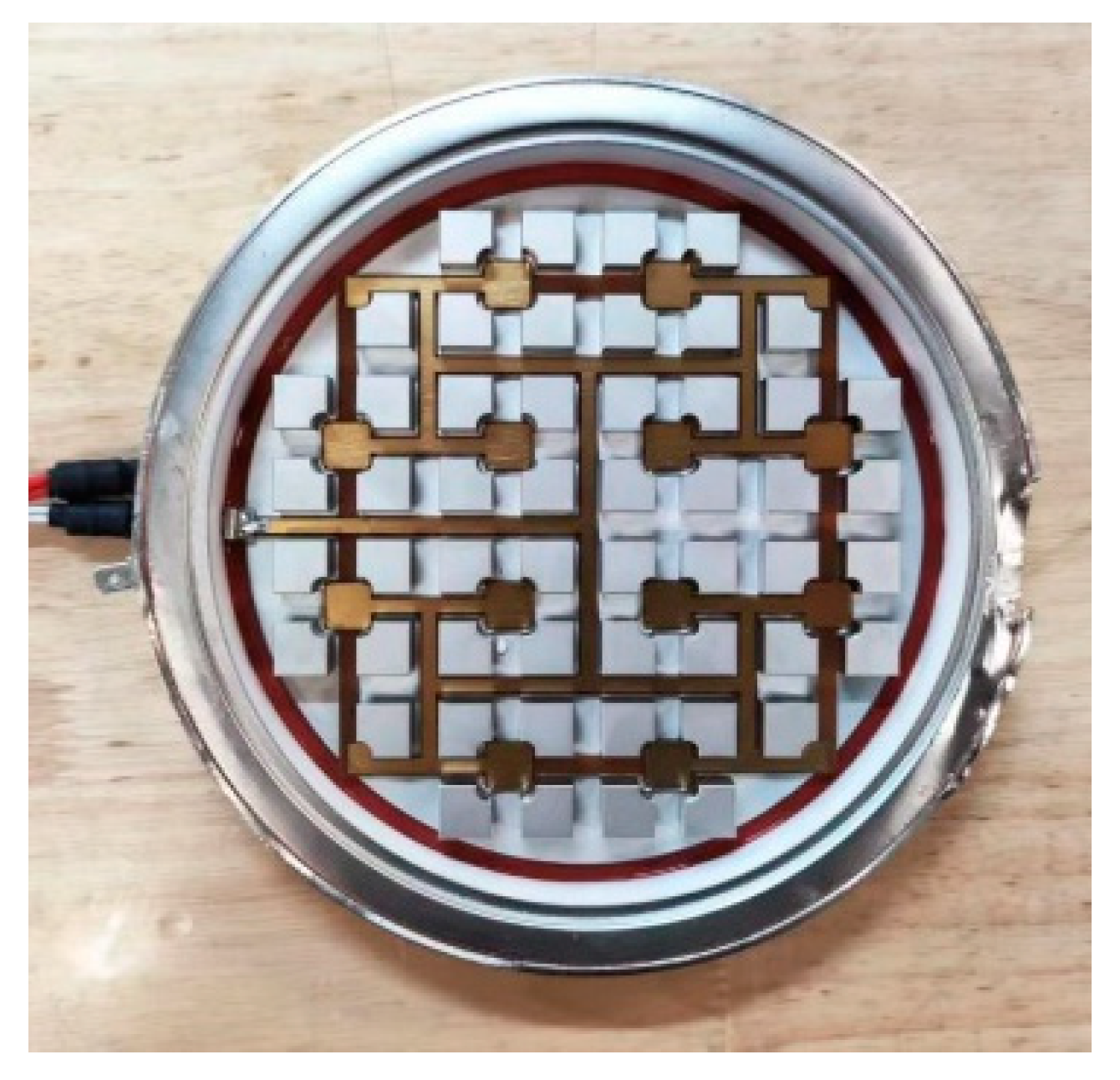
The simulation model was built based on the T2960BB45E crimped IGBT produced by the IXYS Company (Milpitas, CA, USA). The device contained 52 symmetrical and closely arranged chips. Each chip was 1.7 cm × 1.7 cm square, and the outer diameter of the shell was 13 cm. Figure 1 shows a picture of the T2960BB45E.

Figure 1.
T2960BB45E physical internal structure.
Through the structural analysis of common crimped devices, it can be seen that the current path in the crimped device is perpendicular to the upper and lower plates, and the current will pass through the device uniformly and symmetrically under the ideal current sharing state. The state of uniform flow of the unit length current element simulator is set in the center of each chip, and the magnetic field intensity on the x and y sections of the device is calculated with the current direction as the Z-axis and the contours of the field intensity are drawn. For easy observation, the field intensity is divided into internal and external magnetic field results, as shown in Figure 2.
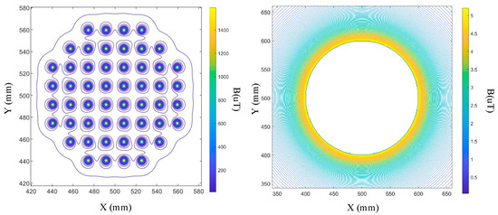
Figure 2.
Intensity of the magnetic field inside and outside the device in the uniform flow state.
In Figure 2, X and Y represent the spatial coordinates of the chip inside the IGBT, B denotes the magnetic flux density, and darker colors indicate higher values of B. Because the current in the device is all in the vertical direction, it can be seen from the right-hand rule that these currents do not contribute to the external magnetic field in the Z-axis direction, and because of the symmetrical chip arrangement method of the crimped device, when all the chips flow uniformly, the magnetic field line outside the device is approximately a positive circle, and the horizontal direction of the magnetic field is perpendicular to the radius everywhere. The magnetic field strength decays with distance from the device.
To simulate the reduction of current density in a specific region, some chips are removed on the left while maintaining the total current constant. After this adjustment, the magnetic field is recalculated. As shown in Figure 3, where The definitions of X, Y, and B in this context are consistent with their meanings in Figure 2, the magnetic field strength decreases near the region where the current density is reduced, while an increase in the magnetic field strength is observed on the opposite side due to the redistribution of the current.
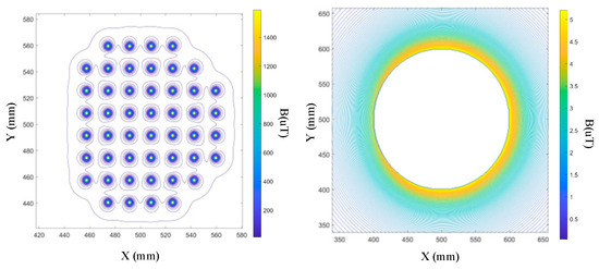
Figure 3.
Intensity of the magnetic field inside and outside the device in one side current missing state.
2.2. Current Sensing Method Based on the Hall Sensor
In order to obtain the magnetic field data near the device, it is necessary to select an appropriate magnetic field sensor. Due to the flat structure of the crimple device and the large metal heat sink pressed up and down, the space around the device close to the tube shell is narrow, so the choice of the magnetic field sensor needs to consider the problem of space arrangement. The small devices suitable for magnetic field measurement on the market are mainly linear Hall sensors.
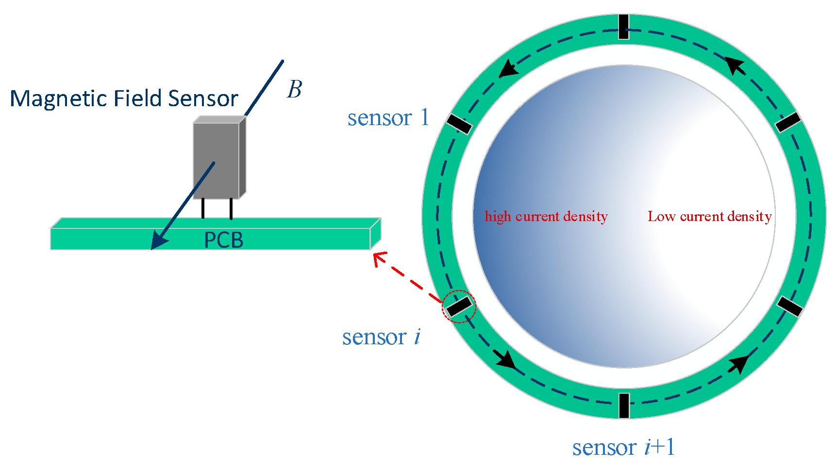
According to the magnetic field analysis, the tangential magnetic field data outside the device close to the device shell is the most valuable for analyzing the current distribution in the device because it has the highest magnetic field value and the largest variation with the current distribution, which is beneficial to cover the external interference. In addition, due to the symmetry of crimp-type devices, the measuring points should be uniformly arranged in a ring on the outside of the device to obtain the information in all directions in a balanced way, as shown in Figure 4, where the arrows denote the magnetic flux through the sensors.
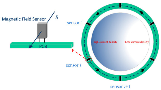
Figure 4.
Magnetic field sensor arrangement method.
Next, the current distribution in the device needs to be analyzed using several key magnetic field values. The design goal of the algorithm is to obtain a vector whose angle indicates the direction in which the current density in the device is significantly larger or smaller than that in the rest of the region and whose modulus indicates the degree of uneven current distribution.
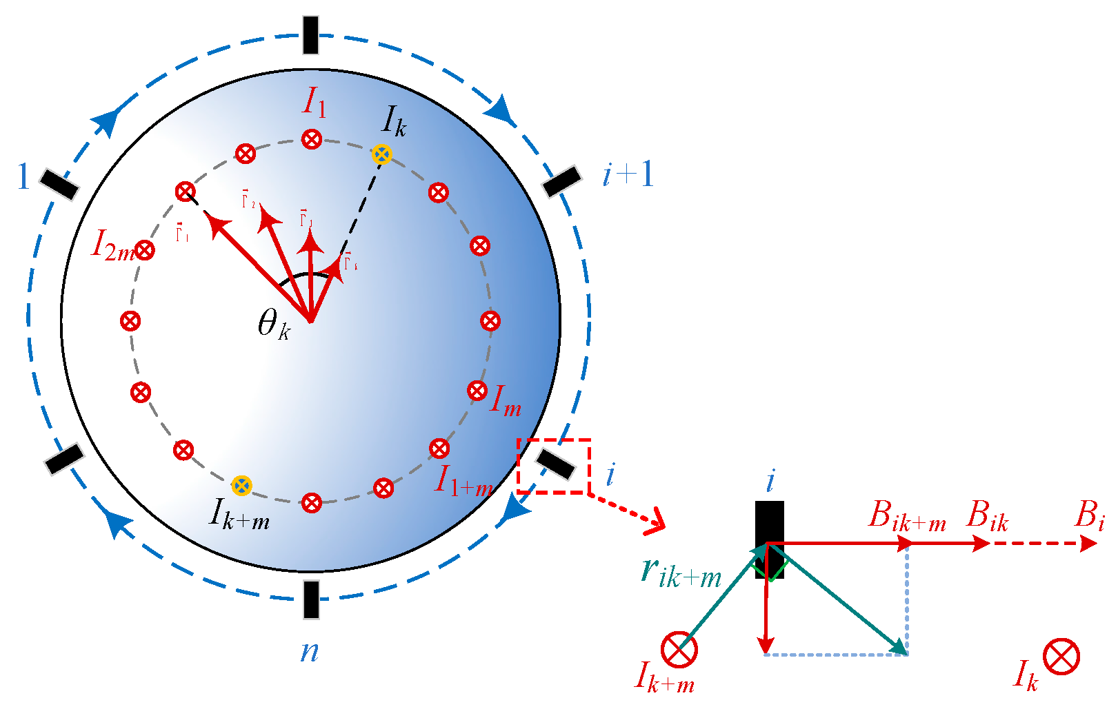
In order to find the direction of the region where the current density changes, it is assumed that there are only two symmetric virtual currents in the device, and , as shown in Figure 5 where Bik represents the magnectic flux generated by the current Ik and the measured magnetic field values are only generated by these two currents. The approximate solution of the two current values can be obtained by solving an overdetermined equation:

Figure 5.
Sensing method for magnetic field inversion of current distribution.
According to the Biot-Savart law, the magnetic field generated by a current element in space can be calculated using the following formula:
where:
is the infinitesimal magnetic field produced by the current element at a point in space.
is the permeability of free space, with a value of .
is the current intensity.
is the length vector of the current element, with its direction aligned with the current flow.
is the position vector from the current element to the measurement point.
is the distance from the current element to the measurement point.
Extending this to multiple magnetic fields and multiple currents, the following matrix form can be obtained:
Since the monitoring method used in this paper involves measuring the magnetic flux density (B) outside the device using Hall sensors to infer the internal current distribution (I), that is, knowing B to solve for I, it is necessary to reformulate the Biot-Savart law to obtain the following equation:
where B is the measured magnetic field value, the number of which should be greater than or equal to two; the number of magnetic field data B will affect the overall calculation accuracy, which will be analyzed later; r is the distance between the magnetic field sensor and the virtual current; and l is the vector indicating the length and direction of the virtual current, its modulus value can be any value, and the direction is the same as the actual current. μ0 is the vacuum permeability. The position of the virtual current should be selected as close to the center of the device as possible to weaken the interference of the weight of the calculation results in different directions caused by the different distance r between the virtual current and the magnetic field measurement point. The difference between the solved virtual current values is defined as:
The value indicates the degree of uneven current distribution in the current position to a certain extent so that the estimation calculation of the uneven current distribution in a direction is completed.
Rotate the position of the virtual current with the center of the device as the symmetry point and repeat the above calculation process at each angle to obtain the corresponding to the angle θk at each angle. At this time, the angle corresponding to the with the largest modulus is the calculated bias direction of the uneven current in the device, and its modulus indicates the degree of unevenness. The modulus values are combined with the information on the angles, and finally, a vector is generated. To ensure the unity of the results, when the value of is negative, the negative sign is considered to be converted into a positive value by adding 180 degrees in the angle when generating the vector, as shown in the following formula:
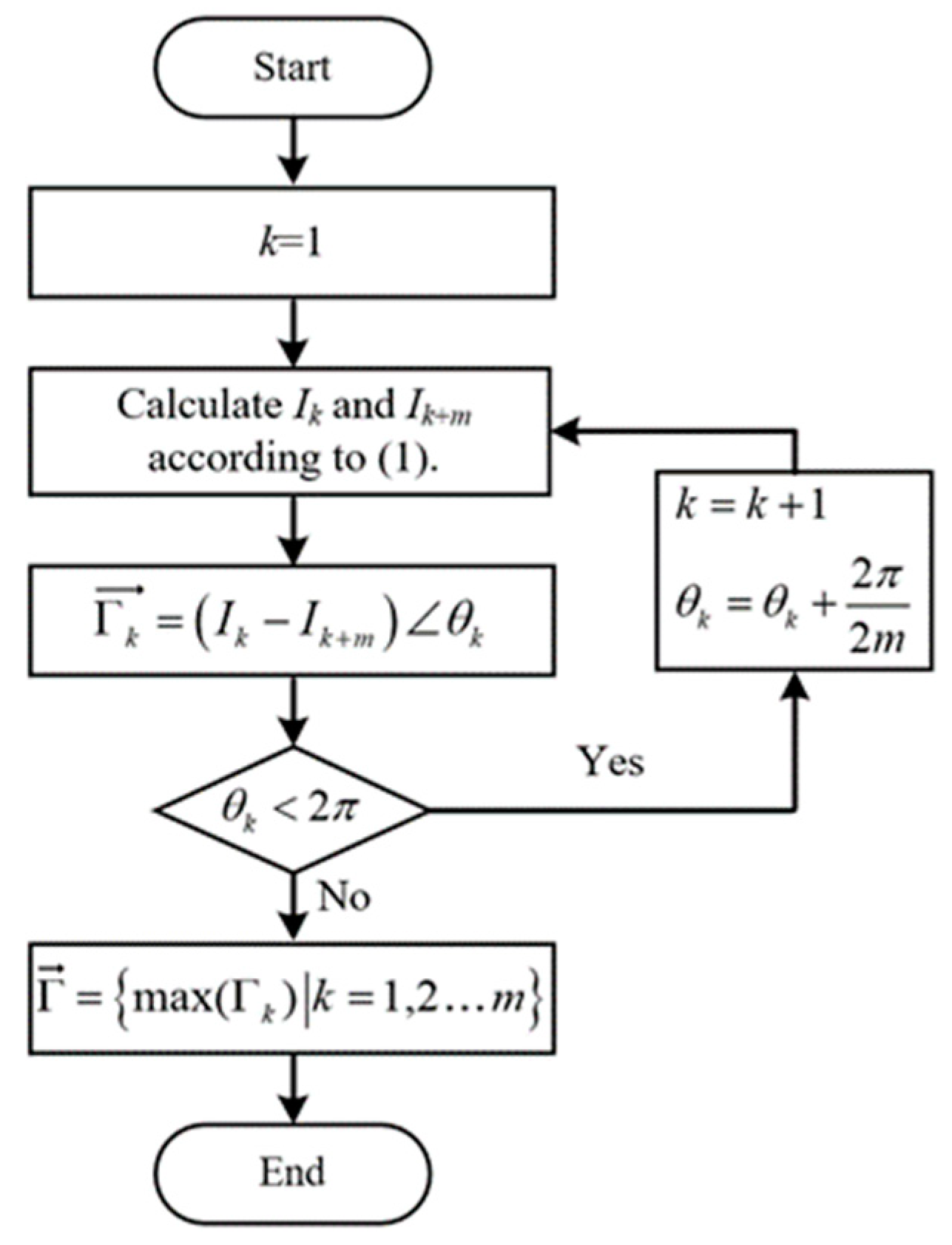
Figure 6 illustrates a flowchart for current calculation based on the Biot-Savart law. This flowchart details how to calculate the maximum value of current using an iterative method. Initially, the variable k is set to 0, and it checks whether the current angle θk is less than 2 π. If it is, the Biot-Savart law is applied to calculate the corresponding currents and , followed by the calculation of the time difference Tk = Ik − Ik+m. Then, θk is updated to θk + , and k is incremented. This process is repeated until θk is no longer less than 2 π. Finally, the maximum value is identified from all calculated time differences, which represents the desired maximum current value .
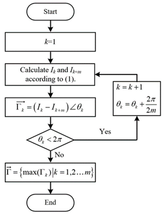
Figure 6.
Flowchart for the maximum current calculation using the Biot-Savart law.
3. Error Analysis and Verification of the Proposed Method
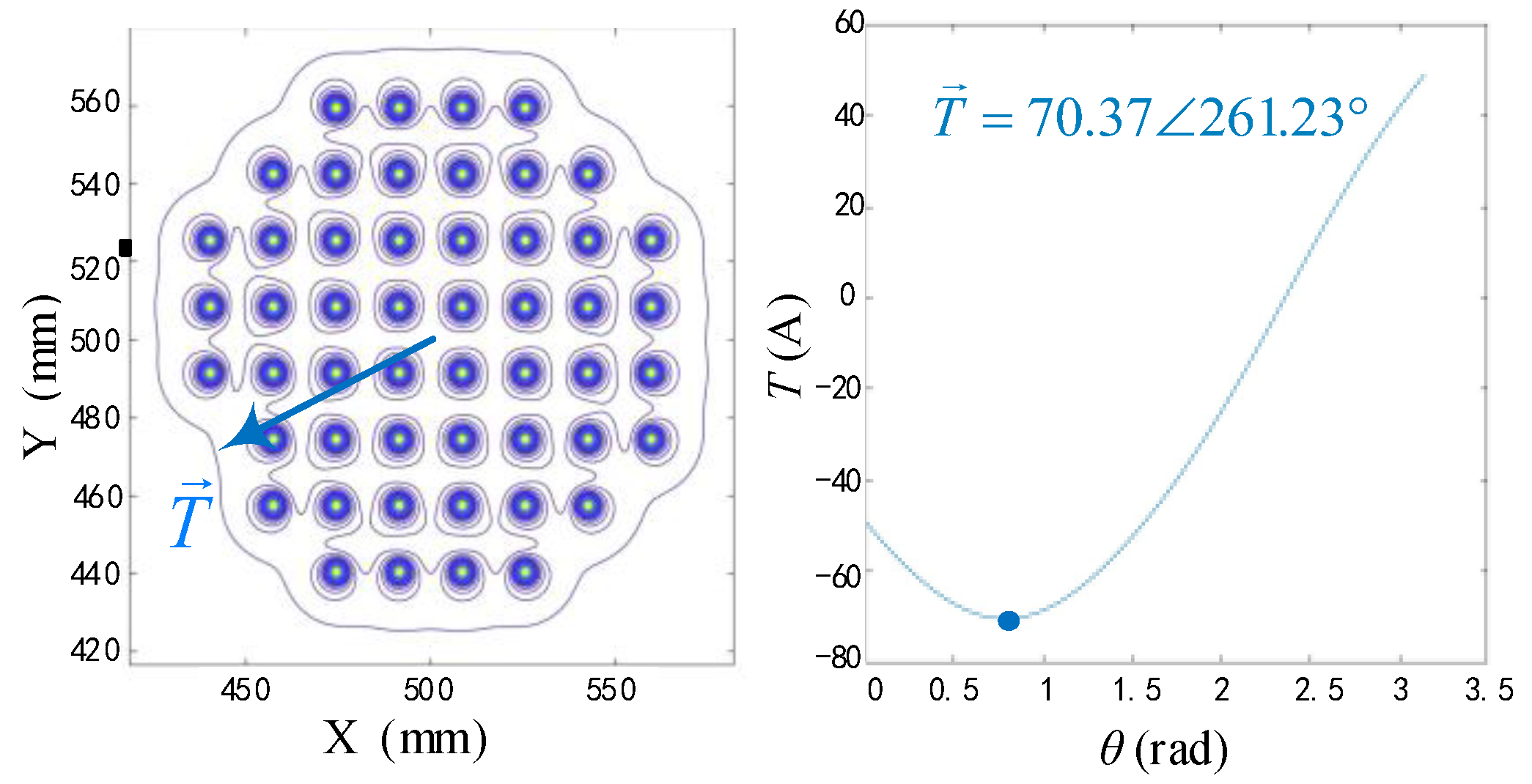
The calculation method proposed above considers only the device itself and the current passing vertically. It solves the overdetermined equation to find the direction of the uneven current distribution. In most current distribution states, the angle indication has certain errors. The simulation results are shown in Figure 7, considering the case of missing one chip at the bottom left as an example. The arrows in Figure 7 represent the direction of the bias current. X and Y represent the spatial coordinates of the chip inside the IGBT. θ indicates the direction of uneven current distribution inside the device and T indicates the degree of uneven current distribution obtained through magnetic field measurements and numerical analysis calculations.
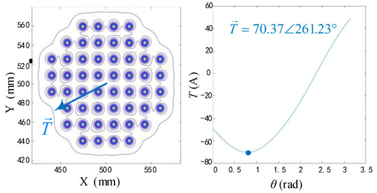
Figure 7.
Calculation result of missing one chip case at the bottom left 1.
Taking (500, 500) as the coordinate center, the center of the missing chip is located at (−59.5, −22.5); using the inverse trigonometric function to calculate the angle of the pinch and then converting it to the reference system with the vertical axis as 0, the angle is 249.28 degrees, and using the solution of the equations to derive the angle corresponding to the maximum offset, is 261.23 degrees, and the difference between the two reaches about 12 degrees.
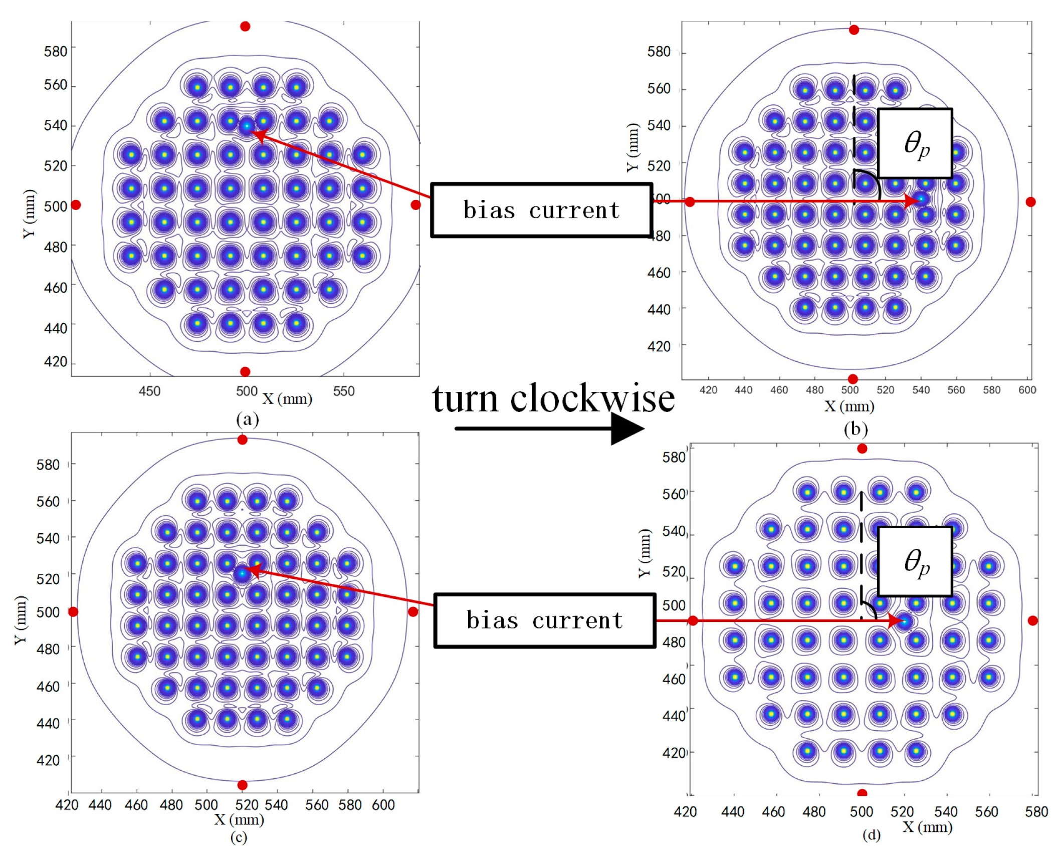
In order to analyze the error at each angle, simulations were performed, as shown in Figure 8. To analyze the prevailing error magnitude and design a correction method, the current distribution state at multiple angles and distances was simulated and analyzed, and the simulation model is shown in Figure 8,where the meanings of X and Y are consistent with those in the previous figure and the position of the bias current has been marked in the picture.
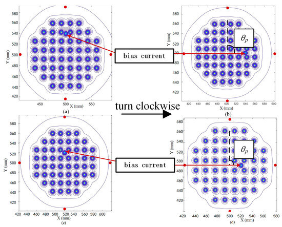
Figure 8.
(a) Bias current is located far above; (b) bias current is located far right; (c) bias current located near the top; (d) bias current located near the right side.
On the basis of setting all the chips to pass current uniformly, an additional bias current is added to the device to adjust the current distribution in the device. The initial state of the bias current is located directly above, and the vertical axis of symmetry angle θp is 0, after the case to keep its distance from the center of the same and change the size of the angle to make it constantly rotate to the right, and finally make it reach the right side of the device at an angle of 90 degrees, such as (a), (b). On the basis of setting all the chips to pass current uniformly, an additional bias current is added to the device to adjust the current distribution in the device.
The initial state of the bias current is located directly above, and the vertical axis of symmetry angle θp is 0, after the case to keep its distance from the center of the same and change the size of the angle to make it constantly rotate to the right, and finally make it reach the right side of the device at an angle of 90 degrees, such as (a), (b). Extract the magnetic field data at each angle θp to calculate the vector , take its angular part θk and the actual bias current is located in the angle θp subtracted from the difference between the two θd, as the error on this angle
In order to exclude the effect of the distance of the bias current from the center, the above calculations were repeated, adjusting its distance from the center as in (c) and (d). Based on the symmetry of the device itself and the symmetry of the measurement point arrangement, it is easy to surmise that the results of the calculations at other angles are the same as the results from 0 to 90 degrees, so only this part of the value is calculated.
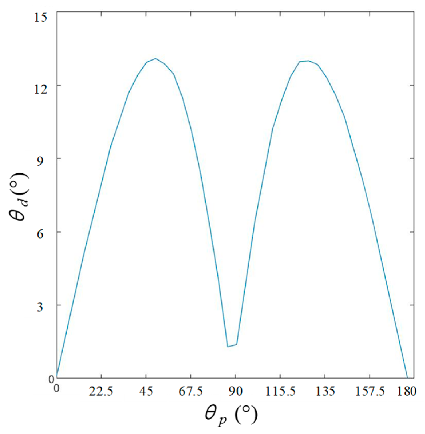
Calculation results (a), (b) group and (c), (d) group are identical to θd as the vertical coordinates, θp as the horizontal coordinates of the results of the calculation of the line graph as shown in Figure 9; from the figure, it can be seen that the bias current is located in the 0 degree, 45 degrees, 90 degrees when the error is almost 0, due to the curve is discrete points and then connected to the line drawn, the number of steps between the number of did not take the 45-degree curve is not over zero here. The curve does not cross zero here. The range of error size was 0 to 45 degrees and 45 degrees to 90 degrees, with the angle of change of approximately two sinusoidal half-waves and a peak error of about 13 degrees, which is consistent with the previous simulation results.
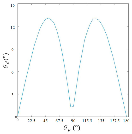
Figure 9.
Calculation results of error at each angle.
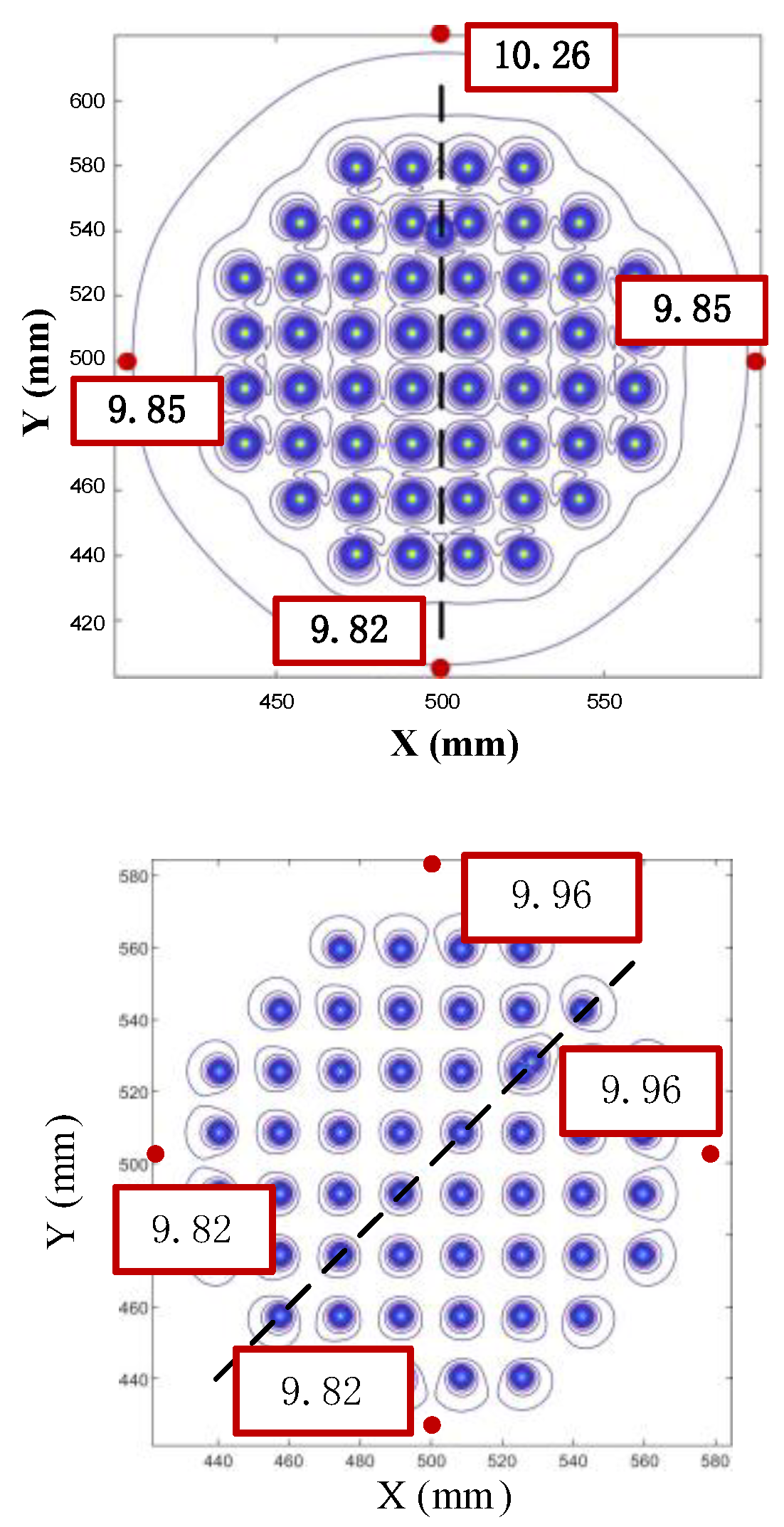
It is easy to understand that the error is close to 0 at 0, 45, and 90 degrees. The bias currents are located at 0 and 45 degrees in both cases, and the positions of the four measurement points with the values of the magnetic field have been labeled, as shown in Figure 10, where X and Y represent the spatial coordinates of the chip inside the IGBT, the numbers represent the magnetic field strength at the corresponding points. The 0-degree and 90-degree directions are directly opposite to the direction of the measurement point arrangement; the opposite measurement point has the maximum or minimum value of the magnetic field; due to the method of the measurement point arrangement being a ring uniform distribution, the remaining measurement points to the actual current offset direction as the axis of symmetry, the two sides of the measurement point of the value of the magnetic field must be the same.

Figure 10.
Magnetic field values of measurement points at special angles.
According to the principle of symmetry, the solution of the equation at each angle has the same symmetrical relationship and will have the largest value in the opposite direction of the offset. For the case of 45 degrees, the principle is the same: the value of the measuring point has symmetry, and the maximum value will be taken in the offset direction. For the remaining angles of the offset current position, there is no longer symmetry between the values of the measurement points, and the calculations will result in varying degrees of error. This will hold true for any number of measurement points.
The above analysis can be summarized as follows: when the direction of the uneven distribution of current in the device is facing any measurement point or any two measurement points of the angular bisector of the computational error is almost 0, the rest of the angle, the error will be a periodic change, the error value of each time over the 0 for a period approximated to the sinusoidal half-wave changes in the peak value of the different number of points can be obtained through the simulation.
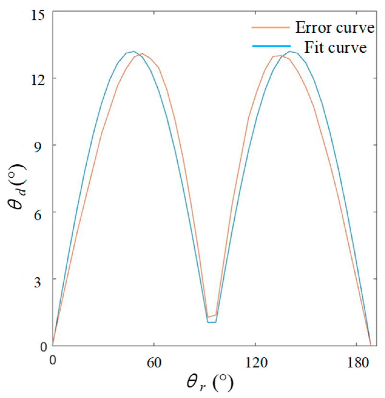
In the previous section, the basic law of the calculation results in the angular error; consider the use of a sinusoidal half-wave to fit the error in each angle to compensate for the corresponding angular value in the previous section of the four measurement points when the calculation results as an example of the original error and the fitted curve plotted together as shown in Figure 11.
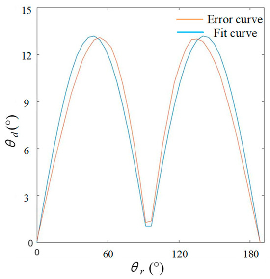
Figure 11.
Error curves with fitted error correction curves.
The blue curve is the sinusoidal function under one cycle of taking the absolute value, and its horizontal coordinate is transformed according to the characteristics of the error distribution at the four measurement points, mapped from 0–2 π to 0–π/2, with the amplitude taken as the peak error value of 13 degrees. The red curve is the error curve, and a high degree of similarity can be seen between the two.
The values of θk are corrected using the fitted sinusoidal halfwave curve, and the values of both are subtracted to obtain the corrected calculation of θ0.
Calculate the mean value of the original error θp in the value under each angle and the mean value of θ0 under each angle and plot the histogram of the two as shown in Figure 12. The error before correction is 7 degrees, of which the peak value is 13 degrees, and after correction is 1 degree, of which the peak value of the error after correction is 2 degrees. The error is cut to one-seventh of the original value, and this method has a good correction effect.
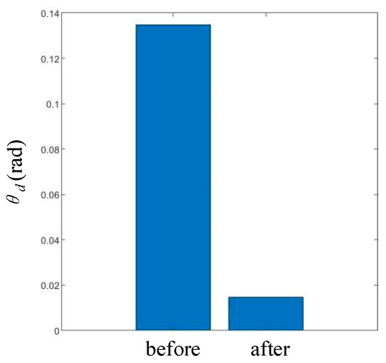
Figure 12.
Comparison of the mean value of error before and after correction.
4. Determination of the Number of Measurement Points
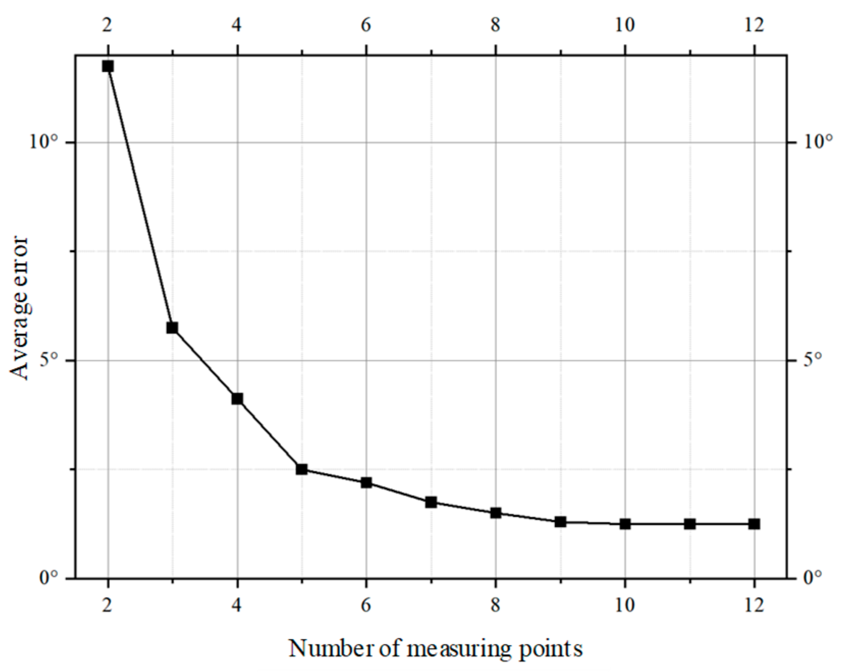
In the following, these methods and conclusions will be synthesized to calculate the accuracy of the current distribution estimation for each number of measurement points and to give a suitable strategy for the selection of the number of magnetic field measurement points.
Still, the simulation model is used in the first section, as shown in Figure 8. For all the chip uniform current download devices, an additional bias current is set up to adjust the current distribution. The magnetic field measurement points are set according to the number of uniformly distributed points from the center of the device, with a radius of 80 mm on the circumference of the tangential direction, to determine the field strength.
For each number of measurement points, the bias current position is adjusted to calculate the current distribution state at each angle and corrected using the method in Section 1 to obtain θ0, and finally, the maximum value of θ0 for all bias currents is taken as the first part of the final error, θ1. Considering the existence of the side bus bar, which is commonly found in engineering practice, and according to the simulation results of Section 2, this result is still affected by the elimination of the interference after taking the difference value; therefore, for each measurement point, the maximum value of the angular error brought by the lateral busbar is calculated in the finite element simulation model as the second part of the final error, θ2, and the final error statistic θ0 is obtained for each measurement point.
Plot the error at each measurement point with the number of measurement points as the horizontal coordinate and the error θ0 as the vertical coordinate.
It can be seen from Figure 13 that although the accuracy with the increase in the number of measurement points gradually improves, the enhancement is getting smaller and smaller, and due to the existence of the mother row interference, there will always be about 1 degree of error that cannot be eliminated. In the ideal state, using the error correction method after the two measurement point errors of about 12 degrees, the accuracy is not low, but considering the actual application of the sensor arrangement of the position deviation, sensor measurement errors, and other issues exist, only the two magnetic field value calculation will lead to the results of the robustness of the poor. Therefore, it is recommended to adopt the program of four measurement points under the premise of sufficient accuracy, both the use of a smaller number of measurement points and a certain amount of data redundancy to absorb the interference in the actual magnetic field measurement and data transmission.
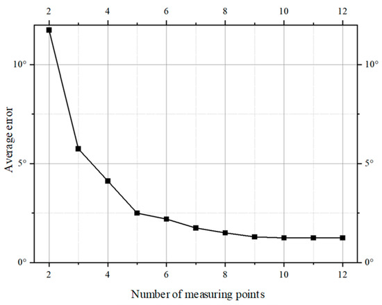
Figure 13.
Average error for different numbers of measurement points.
5. Experimental Validation
5.1. Hall Sensor Selection
In order to meet different measurement needs, sensors of the same series are usually differentiated in range to form different models, while the rest of the parameters are the same. As can be seen from the table, there is little difference in the parameters of nonlinear error and temperature sensitivity drift between the devices of various manufacturers, and their power consumption is between 10 mW and 35 mW. Considering that the magnetic field measurements required by the method of this paper are made outside the device casing and the sensor is placed in the air, the sensor alone will not reach an excessively high operating temperature, and therefore, only the sensor range needs to be paid attention to. The DRV5056 series produced by TI company is only for unipolar magnetic field measurement, and the conventional bipolar measurement sensor of 2.5 V ± 2.5 V voltage output is different, using a wider range of 0.6 V–5 V unidirectional voltage output and has a smaller magnetic field range of 0–200 G, so it has the highest measurement sensitivity. The direction of the magnetic field to be measured in this method is defined, so the DRV5056 is more suitable for this scenario.
The measurement device finally adopts a 4-point solution, with two sensors in each half-ring, and is powered by a commercially available 5V DC power supply, as shown in Figure 14. The locations of each device have been marked in Figure 14. As the output voltage of the linear Hall sensor is directly related to the supply voltage, voltage regulator capacitors are set in the power supply outlet and Hall sensor power supply port to ensure the stability of the power supply. Two layers of PCB boards, in order to minimize the interference between the signals, the power supply circuit on the front side of the board and the signal output on the back side of the board lead out.
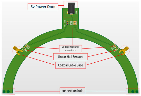
Figure 14.
Magnetic field measurement device design program.
The signal output is connected to the base of the sensor coaxial cable, and the coaxial cable is used to output the voltage signal to the oscilloscope. Holes are punched at both ends of the board, and plastic is used to connect and secure the other half of the ring PCB, which also serves as a support so that the PCB does not come into direct contact with the high-potential heat sink. The specifications of the measurement device are based on the IXYS T2960BB45E as a reference. Crimped IGBTs of the same voltage level from different manufacturers are very close in size, so it is possible to accommodate all the 4.5 kV/3 kA round-case crimped IGBTs that are commonly available on the market today.
Table 2 provides a comprehensive comparison of three major current measurement technologies: Rogowski coils, optical methods, and methods based on shunt resistors. By analyzing their performance in terms of measurement accuracy, intrusiveness, scope of application, anti-interference capability, and cost, the aim is to provide a reference for selecting the most suitable current measurement technology for different application scenarios. Rogowski coils, with their high measurement accuracy and good linearity, are particularly suitable for measuring AC currents, especially high-frequency currents, inrush currents, and transient currents. Optical methods, with a sensitivity of up to 62.57 mV/A and a linear correlation of measurements to standard current probes of up to 0.9971, are applicable for DC to high-frequency current measurements and are noninvasive. Methods based on shunt resistors, such as INA282 and INA3221, with low offset voltage and low gain error, are suitable for a variety of current ranges, including power management products, battery chargers, etc., but are highly affected by electromagnetic interference. In terms of cost, Rogowski coils and methods based on shunt resistors are relatively cheaper, while optical methods are more expensive.
Table 2.
Comparisons of current measurement techniques.
5.2. Experimental Results
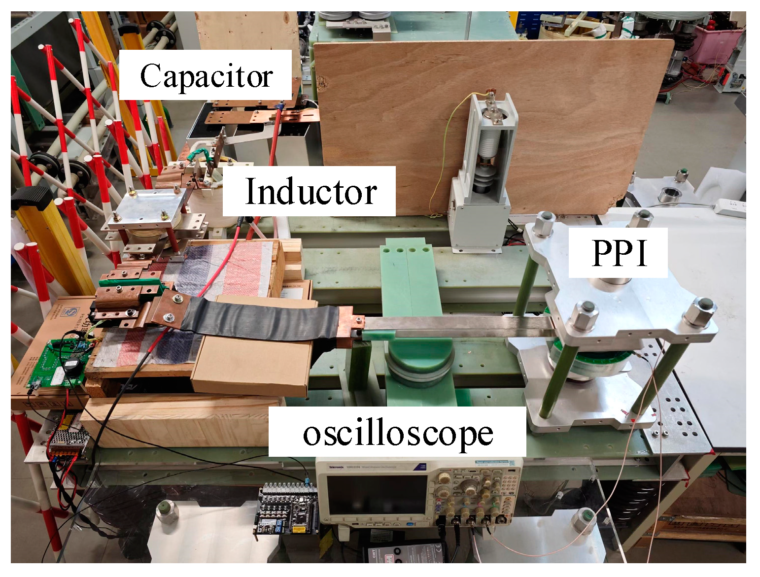
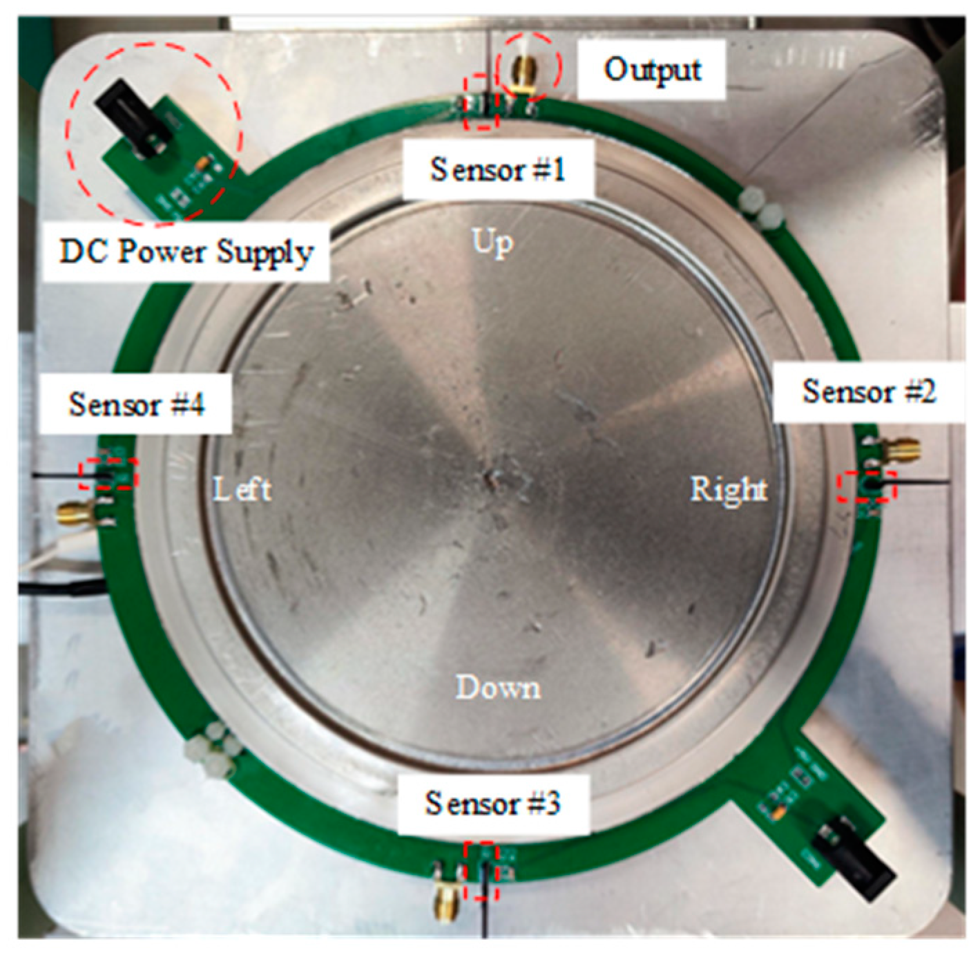
This paper intends to use a double-pulse circuit to conduct experimental verification; the experimental platform physical diagram is shown in Figure 15 [14]. Experiments are totaled under different device current distribution states, and the current distribution in the device is adjusted through the tightness of the four screws above the press-fit structure to influence the offset direction of the pressure on the device. Experiments were conducted in the four directions of uniform pressure on the device, pressure offset to the upper, lower, left, and right, and the four sensors around the device were numbered 1, 2, 3, and 4 for the upper, right, lower, and left, respectively.
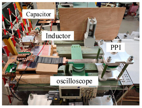
Figure 15.
The device under test and the magnetic field measurement device.
Figure 16 shows the physical setup of the device under test and the magnetic field measurement apparatus. Among them, the output of Sensor #1 corresponds to the CH1 channel of the oscilloscope, the output of Sensor #2 corresponds to the CH2 channel of the oscilloscope, the output of Sensor #3 corresponds to the CH3 channel of the oscilloscope, and the output of Sensor #4 corresponds to the CH4 channel of the oscilloscope. For pressure-contact devices, the greater the applied pressure, the better the conduction performance of the device. That is, under the same voltage conditions, the greater the pressure in a specific region of the device, the larger the current. In the experiment, different pressures were applied to various parts of the device to alter the current distribution, and sensors were used to detect the external magnetic field, thereby inferring the internal current distribution of the device.

Figure 16.
Physical setup of the device under test and the magnetic field measurement apparatus.
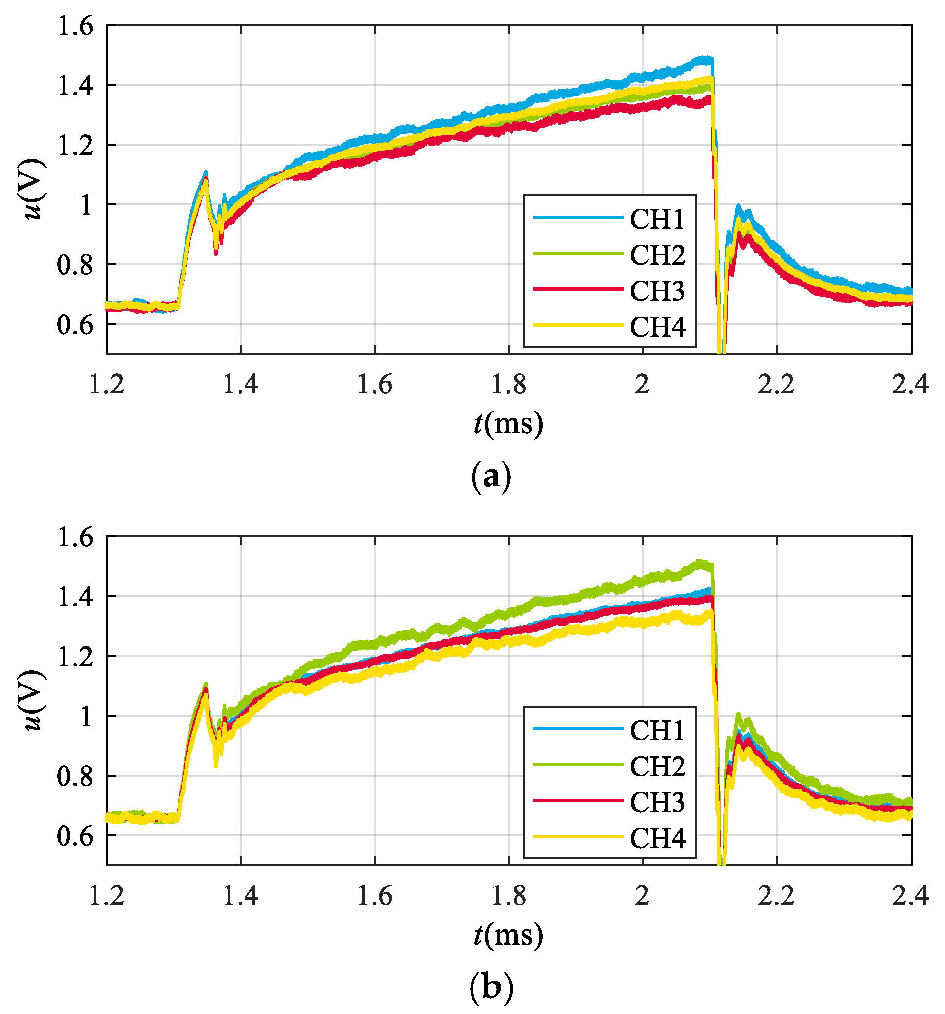
In order to clearly compare the difference of outputs under different pressure conditions, Figure 17 shows the time domain waveforms of the outputs of the four magnetic field sensors around the device under two sets of working conditions: upward bias and rightward bias. It can be seen that when the pressure is upward biased, the current is mainly biased toward the top of the device, and the lower current is small, as in Figure 17a, the value of CH1 is larger than CH3; when the pressure is rightward biased, the current is mainly biased toward the right side of the device, and the left current is small, as in Figure 17b, the value of CH2 is larger than CH4.
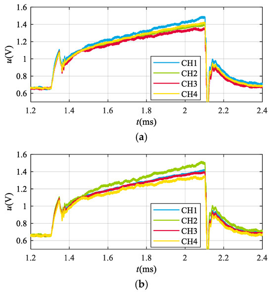
Figure 17.
(a) Output of the magnetic field sensor when the pressure is upward biased; (b) output of the magnetic field sensor when the pressure is rightward biased.
6. Conclusions
In this paper, a nonintrusive current distribution sensing method for crimped devices was investigated through theoretical analysis, simulation, and experimental validation, and the selection method of magnetic field measurement points was obtained by analyzing the current distribution inside the crimped device and the characteristics of the magnetic field outside the device, designing a method for analyzing the current distribution of the crimped device based on the magnetic field data, and proposing a correction method for the computational error of the current distribution sensing method in the ideal state. Finally, the fabrication of the magnetic field measuring device is carried out, and the effectiveness of the method is proved by experiments.
Author Contributions
X.Y.: Conceptualization, Data curation, Formal Analysis, Methodology, Visualization, Writing-original draft, Writing-review & editing; Y.J.: Methodology, Supervision, Validation; W.Y.: Methodology, Supervision; Q.H.: Methodology, Data Curation, Investigation; Z.H.: Methodology, Funding Acquisition; Z.D.: Methodology, Writing-review & editing. All authors have read and agreed to the published version of the manuscript.
Funding
Funded by North China Electric Power Research Institute Co Ltd., grant number KJZ2023116.
Data Availability Statement
Data are contained within the article.
Conflicts of Interest
Authors Xi Yuan, Yirun Ji, Wenqian Yuan, Qing Huai and Zhen Hao were employed by the company North China Electric Power Research Institute Co., Ltd. The remaining authors declare that the research was conducted in the absence of any commercial or financial relationships that could be construed as a potential conflict of interest.
References
- Miao, J.; Zhang, N.; Kang, C.; Wang, J.; Wang, Y.; Xia, Q. Steady-state power flow model of energy router embedded AC network and its application in optimizing power system operation. IEEE Trans. Smart Grid 2018, 9, 4828–4837. [Google Scholar] [CrossRef]
- Wang, M.; Leterme, W.; Chaffey, G.; Beerten, J.; Van Hertem, D. Multi-vendor interoperability in HVDC grid protection: State-of-the-art and challenges ahead. IET Gener. Transmiss. Distrib. 2021, 15, 2153–2175. [Google Scholar] [CrossRef]
- Raju, M.N.; Sreedevi, J.; Mandi, R.P.; Meera, K.S. Modular multilevel converters technology: A comprehensive study on its topologies modelling control and applications. IET Power Electron. 2019, 12, 149–169. [Google Scholar] [CrossRef]
- Furuya, M.; Ishiyama, Y. Current measurement inside press pack IGBTs. Fuji Electron. J. 2002, 75, 1–3. [Google Scholar]
- Bock, B.; Krafft, E.; Steimel, A. Measurement of multiple chip currents in a press-pack IGBT using Rogowski coils. In Proceedings of the 10th European Conference on Power Electronics and Applications, Toulouse, France, 2–4 September 2003; pp. 1–10. [Google Scholar]
- Fu, S.; Li, X.; Lin, Z.; Zhao, Z.; Cui, X.; Tang, X.; Wan, J. Current measurement method of multiple chips using rectangular PCB Rogowski coils integrated in press pack IGBT device. IEEE Trans. Power Electron. 2023, 38, 96–100. [Google Scholar] [CrossRef]
- Jiao, C.; Zhang, Z.; Zhao, Z.; Zhang, X. Integrated Rogowski coil sensor for press-pack insulated gate bipolar transistor chips. Sensors 2020, 20, 4080. [Google Scholar] [CrossRef] [PubMed]
- Shi, Y.; Xin, Z.; Loh, P.C.; Blaabjerg, F. A review of traditional helical to recent miniaturized printed circuit board Rogowski coils for powerelectronic applications. IEEE Trans. Power Electron. 2020, 35, 12207–12222. [Google Scholar] [CrossRef]
- Fu, S.; Zhang, G.; Zhan, Y.; Peng, C.; Zhao, Z.; Li, X.; Cui, X. Method of Segmented Turns Arrangement of PCB Rogowski Coil with Anti-Interference Ability. IEEE Trans. Instrum. Meas. 2021, 70, 9511612. [Google Scholar] [CrossRef]
- Fu, S.; Deng, E.; Peng, C.; Zhang, G.; Zhao, Z.; Cui, X. Method of Turns Arrangement of Noncircular Rogowski Coil with Rectangular Section. IEEE Trans. Instrum. Meas. 2021, 70, 9000310. [Google Scholar] [CrossRef]
- Filsecker, F.; Alvarez, R.; Bernet, S. Comparison of 4.5-kV Press-Pack IGBTs and IGCTs for Medium-Voltage Converters. IEEE Trans. Ind. Electron. 2013, 60, 440–449. [Google Scholar] [CrossRef]
- Qi, L.; Liu, Y.; Zhang, X.; Lu, Y.; Shen, H. Noninvasive Current Distribution Sensing in Press Pack Power Electronic Devices Through Few-Measurement Magnetic Field Analysis. IEEE Trans. Ind. Electron. 2024, 71, 13476–13479. [Google Scholar] [CrossRef]
- Zhuang, W.; Wu, Y.; Wu, Y.; Rong, M.; Wu, X.; Zeng, J.; Tao, C. An Integrated Multichips Package Module With 30 kA Turn-Off Capability Based on Pulse Oscillation for Hybrid Circuit Breaker. IEEE Trans. Ind. Electron. 2024, 71, 6427–6437. [Google Scholar] [CrossRef]
- Peng, C.; Li, X.; Fan, J.; Zhao, Z.; Tang, X.; Cui, X. Experimental Investigations on Current Sharing Characteristics of Parallel Chips Inside Press-Pack IGBT Devices. IEEE Trans. Power Electron. 2022, 37, 10672–10680. [Google Scholar] [CrossRef]


Disclaimer/Publisher’s Note: The statements, opinions and data contained in all publications are solely those of the individual author(s) and contributor(s) and not of MDPI and/or the editor(s). MDPI and/or the editor(s) disclaim responsibility for any injury to people or property resulting from any ideas, methods, instructions or products referred to in the content. |
© 2025 by the authors. Licensee MDPI, Basel, Switzerland. This article is an open access article distributed under the terms and conditions of the Creative Commons Attribution (CC BY) license (https://creativecommons.org/licenses/by/4.0/).